
Timing Generator for Progressive Scan CCD Image Sensor
Description
The CXD2457R is an IC developed to generate the
timing pulses required by Progressive Scan CCD
image sensors as well as signal processing circuits.
Features
· Electronic shutter function
· Supports non-interlaced operation
· Base oscillation frequency 30.0MHz
· Horizontal drive frequency switchable between
15/10/5MHz
· Switchable between FINE (Progressive Scan) mode
or DRAFT (high-frame rate readout) mode
· Vertical driver
Applications
Progressive Scan CCD cameras
Structure
Silicon gate CMOS IC
Applicable CCD Image Sensor
ICX204AK
Absolute Maximum Ratings
· Supply voltage
V
DD
a, V
DD
b, V
DD
c, V
DD
d
Vss 0.5 to Vss + 7.0
V
· Supply voltage
V
SS
VL 0.5 to VL + 10.0
V
· Supply voltage
VH
VL 0.5 to VL + 26.0
V
· Supply voltage
VM
VL 0.5 to VL + 26.0
V
· Input voltage
V
I
Vss 0.5 to V
DD
+ 0.5
V
· Output voltage
V
O
Vss 0.5 to V
DD
+ 0.5
V
· Operating temperature
Topr
20 to +75
°C
· Storage temperature
Tstg
55 to +150
°C
Recommended Operating Conditions
· Supply voltage 1
V
DD
a, V
DD
b, V
DD
c
3.0 to 3.6
V
· Supply voltage 2
V
DD
d
3.0 to 3.6
V
· Supply voltage 3
VH
14.25 to 15.75
V
· Supply voltage 4
VL
9.0 to 5.0
V
· Supply voltage 5
VM
0
V
· Operating temperature
Topr
20 to +75
°C
1
E98113A86-PS
Sony reserves the right to change products and specifications without prior notice. This information does not convey any license by
any implication or otherwise under any patents or other right. Application circuits shown, if any, are typical examples illustrating the
operation of the devices. Sony cannot assume responsibility for any problems arising out of the use of these circuits.
CXD2457R
48 pin LQFP (Plastic)
2
CXD2457R
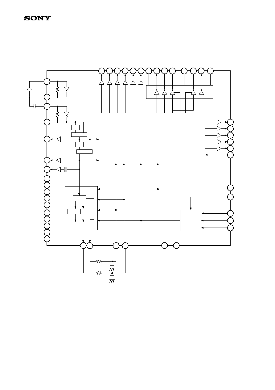
Block Diagram
1
2
3
4
5
6
7
8
9
10
11
12
13
14
15
16
17
18
19
20
21
22
23
24
25
26
27
28
29
30
31
32
33
34
35
36
37
38
39
40
41
42
43
44
45
46
47
48
XSGA and XSGB are readout pulses that use V2A and V2B, respectively, as the VH value.
H
2
AVD1
XCPDM
V-Driver
AVD2
X
S
H
P
X
S
H
D
X
R
S
V
SS
3
PBLK
XCPOB
ADCLK
R
S
T
MCK
V
DD
1
2MCK
TEST2
SEN
SSK
SSI
Register
Pulse Generator
ID
EXP
H
R
O
F
R
O
V
SS
4
H
1
V
SS
2
V
SS
1
R
G
AVD0
T
E
S
T
1
V
DD
0
OSCI
1/3
OSCO
CKI
V
SS
0
CKO
PS
DSGAT
V
L
S
U
B
V
2
B
V
H
V
2
A
V
3
V
1
X
V
2
X
V
3
X
V
1
X
S
U
B
X
S
G
B
X
S
G
A
V
M
F
R
I
H
R
I
1/2
1/1270
SSG
1/3
,
1/792
1/264
3
CXD2457R
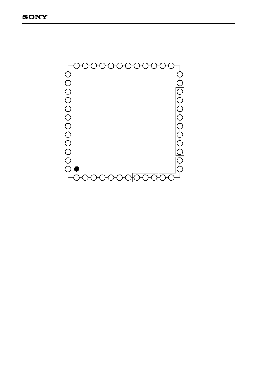
Pin Configuration (Top View)
1
2
3
4
5
6
7
8
9
10
11
12
13
14
15
16
17
18
19
20
21
22
23
24
25
26
27
28
29
30
31
32
33
34
35
36
37
38
39
40
41
42
43
44
45
46
47
48
The enclosed pins use separate power supplies.
H2
AVD1
XCPDM
AVD2
XSHP
XSHD
XRS
V
SS
3
PBLK
XCPOB
ADCLK
RST
M
C
K
V
D
D
1
2
M
C
K
T
E
S
T
2
S
E
N
S
S
K
S
S
I
I
D
E
X
P
H
R
O
F
R
O
V
S
S
4
H
1
V
S
S
2
V
S
S
1
R
G
A
V
D
0
T
E
S
T
1
V
D
D
0
O
S
C
I
O
S
C
O
C
K
I
V
S
S
0
C
K
O
PS
DSGAT
VL
SUB
V2B
VH
V2A
V3
V1
VM
FRI
HRI
4
CXD2457R
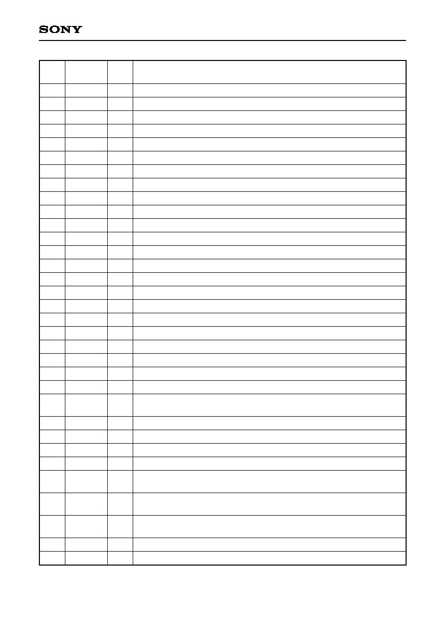
Pin Description
Pin
No.
1
2
3
4
5
6
7
8
9
10
11
12
13
14
15
16
17
18
19
20
21
22
23
24
25
26
27
28
29
30
31
32
33
CKO
Vss0
CKI
OSCO
OSCI
V
DD
0
TEST1
AVD0
RG
Vss1
Vss2
H1
H2
AVD1
XCPDM
AVD2
XSHP
XSHD
XRS
V
SS
3
PBLK
XCPOB
ADCLK
RST
MCK
V
DD
1
2MCK
TEST2
SEN
SSK
SSI
ID
EXP
O
--
I
O
I
--
I
--
O
--
--
O
O
--
O
--
O
O
O
--
O
O
O
I
O
--
O
I
I
I
I
O
O
Oscillator output. (30.0MHz)
GND
Oscillator input. (30.0MHz)
Inverter output for oscillation. (30.0MHz)
Inverter input for oscillation. (30.0MHz)
Power supply.
Test. With pull-down resistor. Fix to low.
Power supply.
Reset gate pulse output.
GND
GND
Clock output for horizontal CCD drive.
Clock output for horizontal CCD drive.
Power supply.
Clamp pulse.
Power supply.
Sample-and-hold pulse.
Sample-and-hold pulse.
Sample-and-hold pulse.
GND
Blanking cleaning pulse.
Clamp pulse.
Clock output for AD conversion.
Reset (Low: Reset, High: Normal operation).
Always input one reset pulse during power-on.
Clock output for digital circuit.
Power supply.
Clock output for digital circuit.
Test. Fix to high.
PS = High: Drive frequency setting input.
PS = Low: Serial setting strobe input.
PS = High: Readout method setting input.
PS = Low: Serial setting clock input.
PS = High: Shutter speed setting input.
PS = Low: Serial setting data input.
Line identification signal output write enable pulse output or XSUB output.
Pulse output indicating exposure is underway or checksum result output.
Symbol
I/O
Description
5
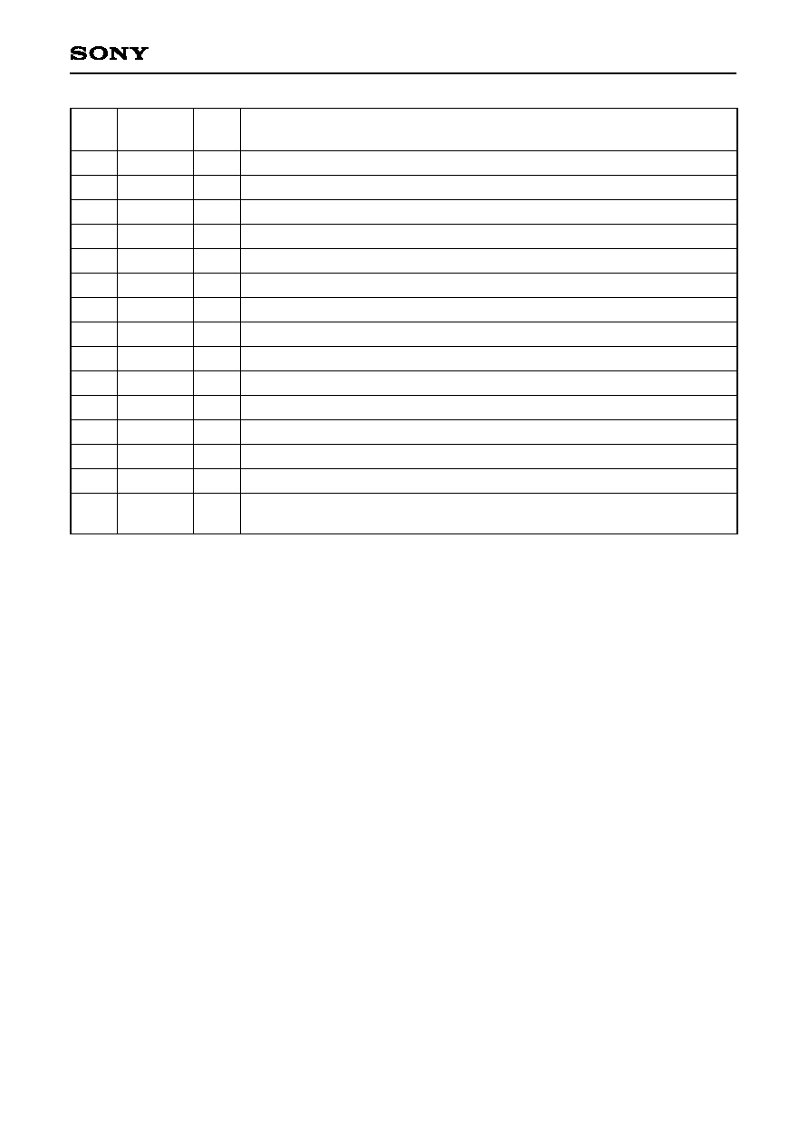
CXD2457R
Pin
No.
34
35
36
37
38
39
40
41
42
43
44
45
46
47
48
HRO
FRO
V
SS
4
HRI
FRI
VM
V1
V3
V2A
VH
V2B
SUB
VL
DSGAT
PS
O
O
--
I
I
--
O
O
O
--
O
O
--
I
I
Horizontal sync signal (HR) output or XSGB output.
Vertical sync signal (FR) output or XSGA output.
GND
Horizontal sync signal (HR) input.
Vertical sync signal (FR) input.
GND (vertical clock driver GND).
Clock output for vertical CCD drive.
Clock output for vertical CCD drive.
Clock output for vertical CCD drive.
15V power supply (vertical clock driver power supply).
Clock output for vertical CCD drive.
CCD electric charge sweep pulse output.
7.5V power supply (vertical clock driver power supply).
Output stop (Same operation control as SLP when low).
Parallel/serial switching for mode setting input method.
(High: Parallel, Low: Serial) With pull-down resistor.
Symbol
I/O
Description