
Ù 1 Ù
CXD2400R
E93308D75-PS
Timing Controller for CCD cameras
Description
The CXD2400R is a timing controller for CCD
camera systems which use the ICX044/045,
ICX054/055 or other black/white CCD image
sensors.
Features
ñ Supports EIA/CCIR standards
ñ Electronic iris (electronic shutter) function
ñ Sync signal generation function
ñ Supports external synchronization
ñ Supports non-interlacing
ñ Supports field/frame
accumulation
ñ Oscillator frequency: 1212 fh
(EIA: 19.0699MHz; CCIR: 18.9375MHz)
The characteristics of CCD image sensors are
guaranteed for field accumulation operation.
Absolute Maximum Ratings (Ta = 25¯C)
ñ Supply voltage
V
DD
Vss Ù 0.5 to
+
7.5
V
ñ Input voltage
V
I
Vss Ù 0.5 to V
DD
+
0.5
V
ñ Output voltage
Vo
Vss Ù 0.5 to V
DD
+
0.5
V
ñ Operating temperature Topr
Ù20 to
+
75
¯C
ñ Storage temperature
Tstg
Ù55 to
+
150
¯C
Recommended Operating Conditions
ñ Supply voltage
5.0V Ý 0.25
V
ñ Operating temperature
Ù20 to
+
75
¯C
Applications
CCD cameras
Structure
Silicon gate CMOS IC
Sony reserves the right to change products and specifications without prior notice. This information does not convey any license by
any implication or otherwise under any patents or other right. Application circuits shown, if any, are typical examples illustrating the
operation of the devices. Sony cannot assume responsibility for any problems arising out of the use of these circuits.
48 pin LQFP (Plastic)
Ù 2 Ù
CXD2400R
45
37
40
38
39
34
42
41
33
27
28
19
43
6
18
31
44
13
14
15
20
21
23
17
22
24
16
29
30
32
36
35
11
9
12
10
7
8
26
25
5
1
3
2
4
48
47
46
LPF
LCIN
LCOUT
L
12
12fH
CKI
AV
SS
H1
H2
AV
DD
RG
SHP
SHD
TG/SSG
GATE
TEST CIRCUIT
IRIS/SHUTTER
CK GEN
GATE
COUNTER
SELECTOR
UP/DOWN ADDER
DECODE
LPF
VIDEO SIG.
1/525
1/625
RESET
GEN
SYNC
SEP
1/2
1/606
XV1
XV2
XV3
XV4
XSG1
XSG2
SYNC
FLD
CBLK
CLP1
CLP2
PS
CVss
SPDNV
/ED2
IRIN
/ED1
SPUPV
/ED0
CV
DD
Vreg
P/S
D
CK
Field/
Frame
O/E
VR1
HD1
HCOMP
EXT
ESYNC
HD
HPLL
VR/SYNC
LSEL
VD
NIL
EIA
FL/FR
V
DD
1V
DD
2
Vss1
Vss2
Vss3
TEST
XSUB
ENB
IRENB
ED0
ED1
ED2
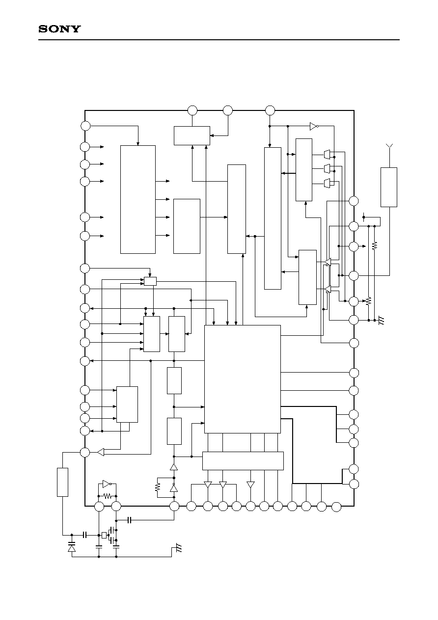
Block Diagram
Ù 3 Ù
CXD2400R
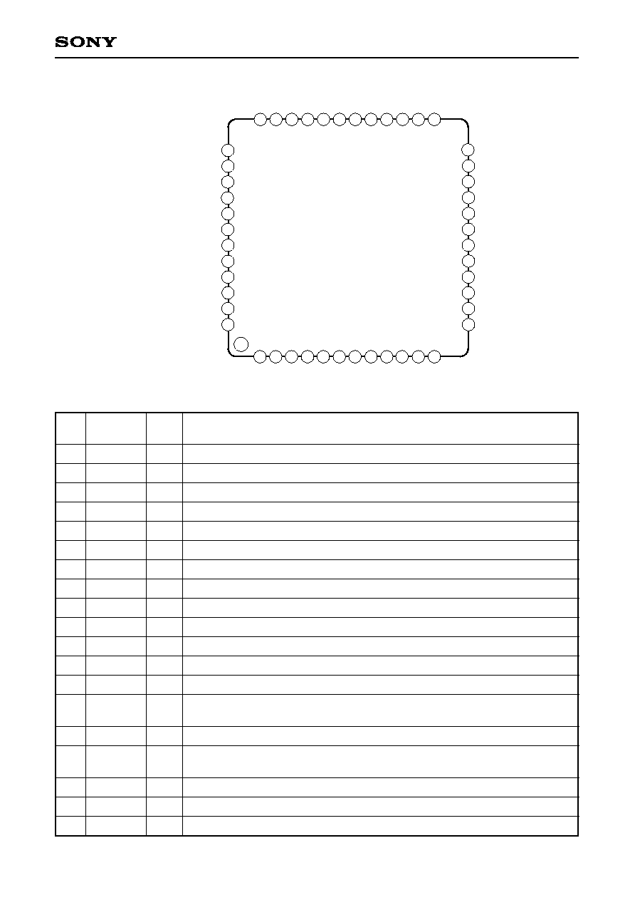
Pin Description
2
3
4
5
6
7
8
9
10
11
12
1
25
26
27
28
29
30
36 35
34
31
32
33
13
14
15
16
17
18
19
20
21
22
23
24
40
39
38
37
41
42
43
44
45
46
47
48
EXT
HPLL
VR/SYNC
ESYNC
NIL
LSEL
V
DD
2
TEST
HCOMP
LCIN
LCOUT
CKI
CV
SS
SPUPV/ED0
SPDNV/ED2
CV
DD
Vreg
V
DD
1
V
SS
2
IRIN/ED1
PS
IRENB
ENB
XSUB
CBLK
SYNC
HD
VD
FLD
V
SS
3
CLP1
CLP2
FL/FR
EIA
SHD
SHP
AV
DD
H1
H2
AV
SS
RG
V
SS
1
XV2
XV1
XSG1
XV3
XSG2
XV4
Pin
No.
1
2
3
4
5
6
7
8
9
10
11
12
13
14
15
16
17
18
19
AV
DD
H1
H2
AVss
RG
Vss1
XV2
XV1
XSG1
XV3
XSG2
XV4
XSUB
ENB
IRENB
PS
IRIN/ED1
Vss2
V
DD
1
--
O
2
O
2
--
O
5
--
O
O
O
O
O
O
O
I
I
I
I
1
--
--
Power supply (for H1, H2)
H1 clock output for CCD horizontal register drive
H2 clock output for CCD horizontal register drive
GND (for H1, H2)
Reset gate pulse output
GND
XV2 clock output for CCD vertical register drive
XV1 clock output for CCD vertical register drive
CCD sensor charge readout pulse output
XV3 clock output for CCD vertical register drive
CCD sensor charge readout pulse output
XV4 clock output for CCD vertical register drive
CCD discharge pulse output
XSUB pulse output ON/OFF control (with pull-up resistance)
Low: XSUB pulse output stop; high: XSUB pulse output
Low: Electronic shutter mode; high: electronic iris mode (with pull-up resistance)
Electronic shutter speed input switchover (with pull-up resistance)
Low: Serial input; high: parallel input
Iris signal input/shutter speed setting; clock input in serial mode.
GND
Power supply
Symbol
I/O
Description
Pin Configuration (Top View)
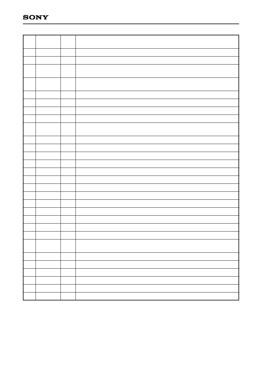
Ù 4 Ù
CXD2400R
20
21
22
23
24
25
26
27
28
29
30
31
32
33
34
35
36
37
38
39
40
41
42
43
44
45
46
47
48
Vreg
CV
DD
SPDNV
/ED2
SPUPV
/ED0
CVss
SHP
SHD
EIA
FL/FR
CLP2
CLP1
Vss3
FLD
VD
HD
SYNC
CBLK
EXT
HPLL
VR/SYNC
ESYNC
NIL
LSEL
V
DD
2
TEST
HCOMP
LCIN
LCOUT
CKI
--
--
I
1
I
1
--
O
1
O
1
I
I
O
O
--
O
O
O
O
O
O
I
I
I
I
I
--
I
O
4
I
2
O
3
I
3
Bias current supply for comparator
Power supply (for comparator)
Shutter speed down reference voltage/
Shutter speed setting; data input in serial mode
Shutter speed up reference voltage/
Shutter speed setting; strobe input in serial mode
GND (for comparator)
Precharge level sample-and-hold pulse
Data sample-and-hold pulse
Low: EIA; high: CCIR (with pull-down resistance)
Field accumulation/frame accumulation, odd field/even field switchover
(with pull-down resistance)
Pulse output for clamp
Pulse output for clamp
GND
Field identification signal output High: odd field; low: even field
Vertical drive output
Horizontal drive output
Composite sync output
Composite blanking output
External sync/internal sync identification signal High: external sync; Low: internal sync
Horizontal drive signal input (with pull-up resistance)
Vertical drive signal input/composite sync input (with pull-up resistance)
Low: SYNC sync or internal sync; high: VD/HD sync (with pull-down resistance)
Low: interlace mode; high: non-interlace mode (with pull-down resistance)
Line number selection pin (with pull-down resistance)
Low: EIA 262H/CCIR 312H; high: EIA 263H/CCIR 313H
Power supply
Fixed to low level (with pull-down resistance)
H comparator output
LC oscillation (crystal oscillator) inverter input
LC oscillation (crystal oscillator) inverter output
Clock input
O
1
POWERED BUFFER
O
2
Hdriver Cell
O
3
OSCILLATOR Cell
O
4
Phase Comparater
O
5
RGdriver Cell
I
1
Comparater Input
I
2
OSCILLATOR Cell
I
3
Input cell with feedback resistance
Pin
No.
Symbol
I/O
Description
Ù 5 Ù
CXD2400R
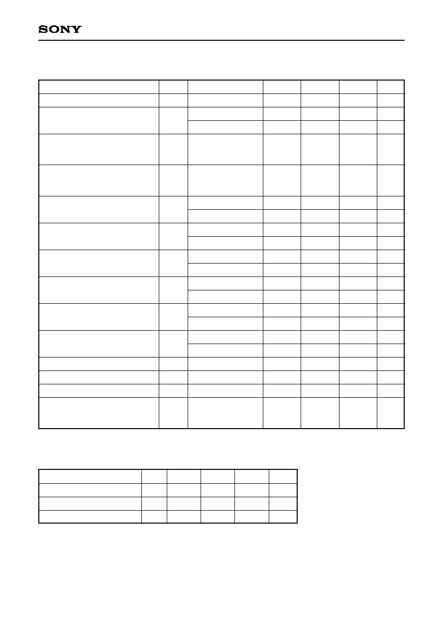
Electrical Characteristics
1) DC Characteristics
(V
DD
= 5V Ý 0.25V, Topr = Ù20 to +75¯C)
Item
Supply voltage
Input voltage 1
(All input pins except those below)
Output voltage 1
(All output pins except those below)
Output voltage 2
(Pins 25, 26)
Output voltage 3
(Pin 5)
Output voltage 4
(Pins 2, 3)
Output voltage 5
(Pin 47)
Output voltage 6
(Pin 45)
Feedback resistance
Pull-up resistance
Pull-down resistance
Current consumption
Input voltage 2
(Pins 22, 23 only in electronic
iris mode)
Input voltage 3
(Pin 17 only in electronic
iris mode)
V
DD
V
IH1
V
IL1
V
OH1
V
OL1
V
OH2
V
OL2
V
OH3
V
OL3
V
OH4
V
OL4
V
OH5
V
OL5
V
OH6
V
OL6
R
FB
R
PU
R
PD
I
DD
V
IN2
V
IN3
I
OH
= Ù2mA
I
OL
= 4mA
I
OH
= Ù4mA
I
OL
= 8mA
I
OH
= Ù8mA
I
OL
= 8mA
I
CH
= Ù20mA
I
CL
= 20mA
I
OH
= Ù3mA
I
OL
= 3mA
I
OH
= Ù4mA
I
OL
= 4mA
V
IN
= Vss or V
DD
V
IL
= 0V
V
IH
= V
DD
V
DD
= 5V
ICX054AL in normal
operating state
4.75
0.7V
DD
V
DD
Ù 0.8
V
DD
Ù 0.8
V
DD
Ù 0.8
V
DD
Ù 0.8
V
DD
/2
V
DD
Ù 0.8
250k
25k
25k
2.0
V
SS
5.0
1M
50k
50k
36
5.25
0.3V
DD
0.4
0.4
0.4
0.4
V
DD
/2
0.4
2.5M
75k
75k
V
DD
V
DD
V
V
V
V
V
V
V
V
V
V
V
V
V
V
V
mA
V
V
Symbol
Conditions
Min.
Typ.
Max.
Unit
Power consumption: 180mW typ., ICX054AL load (in normal operating state)
2) Input/output capacitance
(V
DD
= V
1
= 0V, f
M
= 1MHz)
Item
Input pin capacitance
Output pin capacitance
Input/output pin capacitance
C
IN
C
OUT
C
I/O
9
11
11
pF
pF
pF
Symbol
Min.
Typ.
Max.
Unit

Ù 6 Ù
CXD2400R
Mode Control
Symbol
ENB
IRENB
PS
IRIN/ED1
SPDNV/ED2
SPUPV/ED0
EIA
FL/FR
ESYNC
HPLL
VR/SYNC
NIL
LSEL
EXT
14
15
16
17
22
23
27
28
40
38
39
41
42
37
I
I
I
I
I
I
I
I
I
I
I
I
I
O
XSUB stop
Electronic shutter
Serial input
Electronic iris control signal input pin
(IRENB = high)
Shutter speed setting pin
(IRENB = Low)
EIA
Odd field
Field accumulation
SYNC sync
Internal sync
Internal sync
:
HPLL (Open)
VR/SYNC (Open)
SYNC sync
:
HPLL (Open)
VR/SYNC (SYNC input)
VD/HD sync
:
HPLL (HD input)
VR/SYNC (VD input)
Interlace
EIA
:
262H
CCIR
:
312H
Internal sync
XSUB output
Electronic iris
Parallel input
Valid only when ENB is high.
Valid only when ENB is
high and IRENB is low.
Valid only when NIL is high
and EXT is low.
All other modes.
Valid only when EXT is low.
Valid only when EXT is low
and NIL is high.
Switchover between
internal and external sync
is autonatically identified
by input state at Pins 38,
39 and 40.
Valid only when ENB is
high.
CCIR
Even field
Frame accumulation
VD/HD sync
Non-interlace
EIA
:
263H
CCIR
:
313H
External sync
Pin
No.
I/O
Low
High
Remarks
The characteristics of CCD image sensors are quaranteed for field acccumulation operation.
3) Comparator characteristics
(V
DD
= 5V Ý 0.25V, Topr = Ù20 to +75¯C)
Item
Input offest voltage
Indefinite region
V
OS
Vf
50
Ý 10
mV
mV
Symbol
Min.
Typ.
Max.
Unit
Note) 1. Input offset voltage and indefinite region
Input offset voltage and indefintie region are
existed in the comparator which builds in this IC
as shown right figure. Note that this when
designing external circuit.
2. Pins 22 and 23 for electronic iris mode
Use it in this state of Pin 22 (SPDNV) > Pin 23
(SPUPV).
10mV
10mV
10mV
10mV
Input offset voltage
Input offset voltage
50mV
50mV
5.0V
GND
Indefinite region
Indefinite region
Pins 22 and 23
(SPDNV and SPUPV)
Ù 7 Ù
CXD2400R
Mode Tables
1) Internal sync mode
HPLL pin (Pin 38)
VR/SYNC pin (Pin 39)
ESYNC pin (Pin 40)
: Open
: Open
: Open
Interlace
Field
readout
XSUB pulse OFF
1
Electronic shutter ON
Electronic iris ON
O
O
O
O
O
O
O
O
O
æ
æ
æ
O
O
O
æ
æ
æ
Frame
readout
3
Field
readout
Frame
readout
3
Field
readout
Frame
readout
3
Non-interlace
Odd field
2
Even field
2
1
EIA for 1/60 s accumulation; CCIR for 1/50 s accumulation
2
Line number is 262H or 263H for EIA and 312H or 313H for CCIR.
3
The characteristics of CCD image sensors are guaranteed for field accumulation operation.
O: Can be used.
æ
: Cannot be used.
2) SYNC sync (external sync) mode
HPLL pin (Pin 38)
VR/SYNC pin (Pin 39)
ESYNC pin (Pin 40)
: Open
: SYNC input
: Open
Interlace
Field
readout
XSUB pulse OFF
1
Electronic shutter ON
Electronic iris ON
O
O
O
O
O
O
æ
æ
æ
æ
æ
æ
æ
æ
æ
æ
æ
æ
Frame
readout
3
Field
readout
Frame
readout
3
Field
readout
Frame
readout
3
Non-interlace
Odd field
2
Even field
2
1
EIA for 1/60 s accumulation; CCIR for 1/50 s accumulation
2
Line number is 262H or 263H for EIA and 312H or 313H for CCIR.
3
The characteristics of CCD image sensors are guaranteed for field accumulation operation.
O: Can be used.
æ
: Cannot be used.
Ù 8 Ù
CXD2400R
3) VD/HD sync (external sync) mode
HPLL pin (Pin 38)
VR/SYNC pin (Pin 39)
ESYNC pin (Pin 40)
: HD input
: VD input
: V
DD
(power supply)
Interlace
Field
readout
XSUB pulse OFF
1
Serial input
electronic shutter ON
Parallel input
electronic shutter ON
Electronic iris ON
O
O
O
O
O
O
O
O
O
O
O
æ
æ
æ
æ
O
O
O
æ
æ
æ
æ
O
æ
æ
æ
æ
æ
æ
æ
Frame
readout
3
Field
readout
Frame
readout
3
Field
readout
Frame
readout
3
Field
readout
Frame
readout
3
Non-interlace
VD input with
longer cycle than
normal interlace
VD input with normal cycle
Odd field
2
Even field
2
1
EIA for 1/60 s accumulation; CCIR for 1/50 s accumulation
2
Line number is 262H or 263H for EIA and 312H or 313H for CCIR.
3
The characteristics of CCD image sensors are guaranteed for field
accumulation operation.
Note) Only in the VD/HD sync mode, the external synchronization is possible during which VD pulses with
longer cycle than normal are input to the VR/SYNC pin.
O: Can be used.
: The shutter speed may change
from its value in the interlace mode.
æ
: Cannot be used.
Ù 9 Ù
CXD2400R
Electronic Shutter/Iris
By setting ENB pin (Pin 14) high, the XSUB pulse is output for a specific period to activate the electronic
shutter and electronic iris.
1) Electronic iris (IRENB = high, PS = any level)
Symbol
IRIN/ED1
SPDNV/ED2
SPUPV/ED0
17
22
23
Iris signal input
Shutter speed down reference voltage
Shutter speed up reference voltage
Pin No.
Function
2) Parallel input electronic shutter (IRENB = low, PS = high)
Symbol
SPUPV/ED0
IRIN/ED1
SPDNV/ED2
Shutter speed
23
17
22
H
H
H
EIA:
1/100
CCIR:
1/120
L
H
H
1/250
H
L
H
1/500
L
L
H
1/1000
H
H
L
1/2000
L
H
L
1/5000
H
L
L
1/10000
L
L
L
1/100000
Pin No.
Mode

Ù 10 Ù
CXD2400R
AC Characteristics
SPDNV/ED2
IRIN/ED1
SPUPV/ED0
ts2
th2
ts1
ts0
tw0
Symbol
ts2
th2
ts1
tw0
ts0
20ns
20ns
20ns
20ns
20ns
--
--
--
50çs
--
SPDNV (ED2) setup time for IRIN (ED1) rise
SPDNV (ED2) hold time for IRIN (ED1) rise
IRIN (ED1) setup time for SPUPV (ED0) rise
SPUPV (ED0) pulse width
SPUPV (ED0) setup time for IRIN (ED1) rise
Min.
Max.
1/100000
1/10000
1/5000
1/2000
1/1000
1/500
1/250
1/100
00h
4Ah
65h
82h
97h
A7h
C5h
E1h
1/80000
1/10000
1/5000
1/2000
1/1000
1/500
1/250
1/120
shutter speed
Load value
shutter speed
CCIR
3) Serial input electonic shutter (IRENB = low, PS = high)
Serial input data format
SPDNV/ED2
IRIN/ED1
SPUPV/ED0
D7
D6
D5
D4
D3
D2
D1
D0
The ED2 data is latched in the register at the ED1 rise, and retrieved internally at the ED0 rise.
Typical shutter speed
EIA
Load value
00h
4Eh
6Ah
87h
9Ch
ACh
CAh
EDh
Ù 11 Ù
CXD2400R
External Synchronization
1) External/internal sync selection
External or internal synchronization is selected automatically by a combination of 3 pins (VR/SYNC, HPLL and
ESYNC) to which the sync signal is input externally. The table below shows the input pattern combinations.
Note) Operation is possible even if the VD cycle of the VD input in the VD/HD sync mode is longer than normal.
The EXT pin is the external/internal sync identification signal output pin. This output signal can be used as the
signal to select LC oscillation for expanding the lock range for external synchronization or the oscillator for
improving the oscillation accuracy for internal synchronization.
2) Modes for external synchronization
The characteristics of CCD image sensors are guaranteed for field accumulation operation.
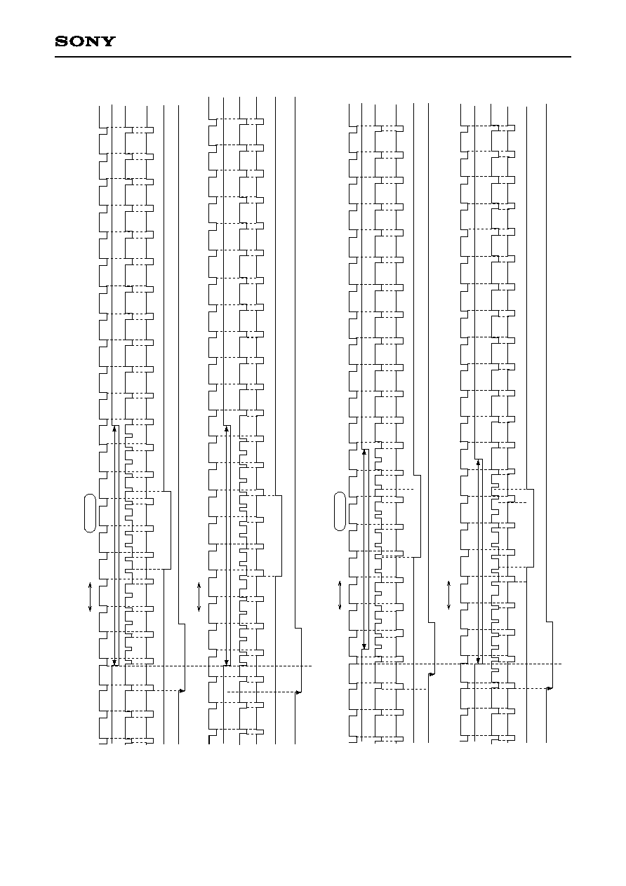
3) Reset operation
SYNC synchronization
The VR1 signal component is extracted from the SYNC signal supplied externally and, for EIA, V reset is
performed so that the VDO pulse falls at the count of 259H (262.5 Ù 3.5H) from the fall of the VR1 pulse. For
CCIR, it is reset in such a way that the VDO pulse falls at the count of 309H (312.5 Ù 3.5H). For these reasons,
it is a prerequisite that the SYNC signal input comply with the EIA or CCIR standard.
VD/HD synchronization
V reset is performed so that the VDO pulse falls 1H later after detecting the fall of the VD (VDR) pulse supplied
externally. Therefore, this enables V reset operation regardless of the field line number. The phase difference
between the VDR pulse and HDO pulse which is locked horizontally at PLL circuit identifies whether the field is
odd or even. (VDR must have a pulse width of 2H or more.)
Input pattern
EXT pin output
Sync state
VR/SYNC pin: SYNC signal
HPLL pin: Open
ESYNC pin: Open
High
External sync
VR/SYNC pin: VD signal
HPLL pin: HD signal
ESYNC pin: V
DD
(power supply)
High
External sync
VR/SYNC pin: Open
HPLL pin: Open
ESYNC pin: Open
Low
Internal sync
SYNC
synchronization
Interlace
Non-interlace
Field accumulation
O
æ
(Cannot be accomplished
since interlace operation
is the prior condition.)
O
O
Frame accumulation
O
æ
(Cannot be accomplished
since interlace operation
is the prior condition.)
O
æ
(Not practically applicable since
the sensitivity is halved.)
Interlace
Non-interlace
VD/HD
synchronization
Ù 12 Ù
CXD2400R
FIELD. E
FIELD. O
EIA
FIELD. O
FIELD. E
HDO
VDO
SYNC
HD1
VR1
VDR
HDO
VDO
SYNC
HD1
VR1
VDR
FIELD. E
FIELD. O
CCIR
FIELD. O
FIELD. E
HDO
VDO
SYNC
HD1
VR1
VDR
HDO
VDO
SYNC
HD1
VR1
VDR
7.5H
7.5H
9H
9H
External Synchronization Reset Operation

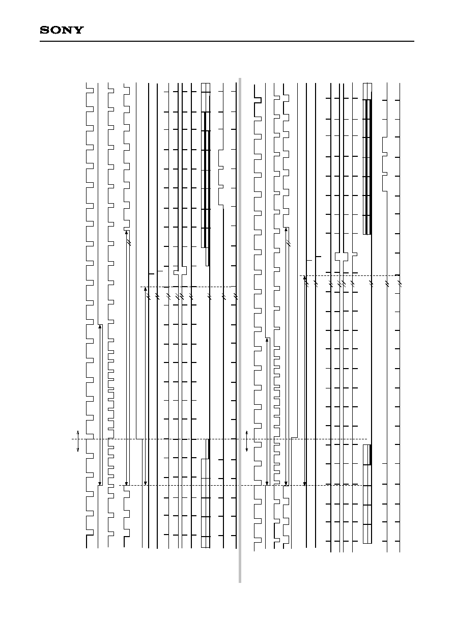
Ù 13 Ù
CXD2400R
FIELD. E
FIELD. O
FIELD. O
FIELD. E
9H
20H
491
492
493
2
3
1
9H
20H
492
493
3
4
2
1
HDO
VDO
SYNC
BLKO
FLD
XSG1
XSG2
XV1
XV2
XV3
XV4
CCD. OUT
CLP1
CLP2
HDO
VDO
SYNC
BLKO
FLD
XSG1
XSG2
XV1
XV2
XV3
XV4
CCD. OUT
CLP1
CLP2
TG+SG Timing Chart
V derection, EIA
Ù 14 Ù
CXD2400R
582
583
25H
FIELD. E
FIELD. O
7.5H
25H
581
582
7.5H
2
1
HDO
VDO
SYNC
BLKO
FLD
XSG1
XSG2
XV1
XV2
XV3
XV4
CCD. OUT
CLP1
CLP2
HDO
VDO
SYNC
BLKO
FLD
XSG1
XSG2
XV1
XV2
XV3
XV4
CCD. OUT
CLP1
CLP2
14.5H
583
2
3
1
FIELD. O
FIELD. E
14H
TG+SG Timing Chart
V derection, CCIR
Ù 15 Ù
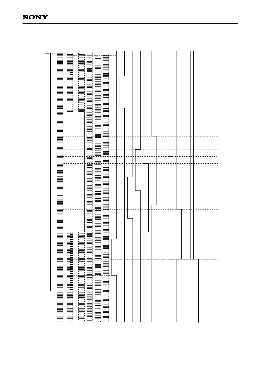
CXD2400R
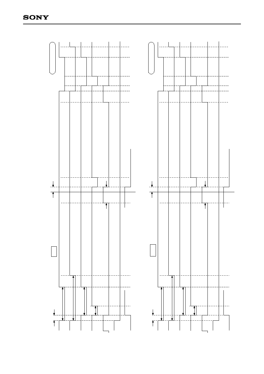
TG+SG Timing Chart
H derection, EIA
Black areas show OB output timing of CCD (ICX044/ICX054).
10
20
30
40
50
60
70
80
90
100
104
MCK = 104.87ns
103
94
80
72
3
50
32
62
44
26
38
73
55
59
14
14
14
14
36
HD/BLK
MCK
H1
H2
RG
SHP
CLP1
CLP2
XV1
XV2
XV3
XV4
XSUB
HSYNC
EQ
VSYNC
FLD
VD
SHD
68
56

Ù 16 Ù
CXD2400R
TG+SG Timing Chart
H derection, CCIR
Black areas show OB output timing of CCD (ICX045/ICX055).
10
20
30
40
50
60
70
80
90
100
114
59
MCK = 105.6ns
107
98
84
72
3
55
37
67
49
61
31
43
73
77
60
59
14
14
14
14
36
HD/BLK
MCK
H1
H2
RG
SHP
SHD
CLP1
CLP2
XV1
XV2
XV3
XV4
XSUB
HSYNC
EQ
VSYNC
FLD
VD

Ù 17 Ù
CXD2400R
E: EIA 1CK = 104.87ns
C: CCIR 1CK = 105.6ns
E: 2.51ç
s
C: 2.53ç
s
(24CK)
E: 38.38ç
s
C: 38.65ç
s
(366CK)
(3CK)
E: 0.315ç
s
C: 0.317ç
s
HD
XSG1
XSG2
XV1
XV2
XV3
XV4
ODD
XV1
XV2
XV3
XV4
EVEN
(12CK)
E: 1.26ç
s
C: 1.27ç
s
E: 1.57ç
s
C: 1.58ç
s
(15CK)
E: 1.99ç
s
C: 2.0ç
s
(19CK)
TG+SG Timing Chart
Charge Readout Timing
Field accumulation
Ù 18 Ù
CXD2400R
E: EIA 1CK = 104.87ns
C: CCIR 1CK = 105.6ns
E: 2.51ç
s
C: 2.53ç
s
(24CK)
E: 39.64ç
s
C: 39.92ç
s
(378CK)
(3CK)
E: 0.315ç
s
C: 0.317ç
s
HD
XSG1
XSG2
XV1
XV2
XV3
XV4
ODD
XV1
XV2
XV3
XV4
EVEN
TG+SG Timing Chart
Charge Readout Timing
Frame accumulation
The characteristics of CCD image sensors are guaranteed for field accumulation operation.

Ù 19 Ù
CXD2400R
TG+SG Timing Chart
ICX054AL
CK
H1
RG
SHP
SHD
CCD OUT
52.4ns (EIA)
52.8ns (CCIR)
26.2ns (EIA)
26.4ns (CCIR)
Ù 20 Ù
CXD2400R
1.468ç
s (14CK)
6.187ç
s
(59CK)
10.9ç
s
(104CK)
4.72ç
s
(45CK)
2.3ç
s
(22CK)
4.72ç
s (45CK)
1.468ç
s (14CK)
1/2H
EIA
1CK = 104.87ns
HDO
BLKO
HSYNC
EQ
VSYNC
VD
FLD
1.478ç
s (14CK)
6.23ç
s
(59CK)
12.04ç
s
(114CK)
4.75ç
s
(45CK)
2.3ç
s
(22CK)
4.75ç
s (45CK)
1.478ç
s (14CK)
1/2H
CCIR
1CK = 105.6ns
HDO
BLKO
HSYNC
EQ
VSYNC
VD
FLD
TG+SG High-Speed Phase Timing Chart
H effective period
Ù 21 Ù
CXD2400R
2.2k
24
21
25
30
4
29
20
27
2
3
4
5
6
7
8
9
10
11
12
13
14
15
16
17
18
19
20
21
22
23
24
25
26
28
29
30
40
39
38
37
36
35
34
31
32
33
41
42
43
44
45
46
47
48
1
VIDEO OUT
IRIS
CXA1310AQ
50k
50k
0.1ç
36k
6.8
ç
/6.3V
0.1ç
150k
2SC3355
10k
270k
2SC945
3.9k
CCD OUT
CXD1250M/N
250K-pixel B/W CCD
RG ADJ
VSUB
ADJ
0.1ç
6.8ç
/6.3V
2.2k
2.2k
47p
47p
47p
47p
2.2k
100
100
SYNC IN
0.1ç
6.8ç
/6.3V
1000p
470
33p
7p
10p
270p
2.7ç
H
7p
0.01ç
100k
0.01ç
1T33C
10k
2.2k
1.5ç
/25V
CXD2400R
27
6.8
ç
/6.3V
0.15ç
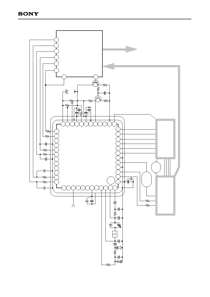
Application
<Sync input external synchronization + CCD iris mode>
Application circuits shown are typical examples illustrating the operation of the devices. Sony cannot assume responsibility for
any problems arising out of the use of these circuits or for any infringement of third party patent and other right due to same.
Ù 22 Ù
CXD2400R
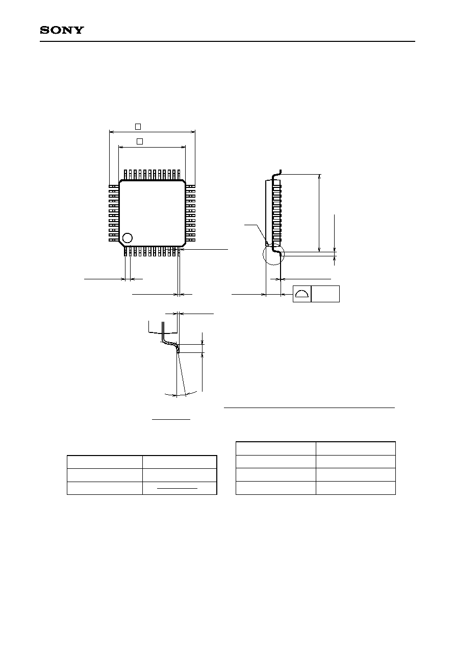
Package Outline
Unit: mm
SONY CODE
EIAJ CODE
JEDEC CODE
PACKAGE MATERIAL
LEAD TREATMENT
LEAD MATERIAL
PACKAGE MASS
EPOXY RESIN
PLATING
42/COPPER ALLOY
PACKAGE STRUCTURE
48PIN LQFP (PLASTIC)
9.0 Ý 0.2
7.0 Ý 0.1
1
12
13
24
25
36
37
48
(0.22)
0.18 Ù 0.03
+ 0.08
0.5 Ý 0.08
(8.0)
0.5 Ý
0.2
0.127 Ù 0.02
+ 0.05
0.1 Ý 0.1
0.5 Ý
0.2
A
1.5 Ù 0.1
+ 0.2
0¯ to 10¯
DETAIL A
0.2g
LQFP-48P-L01
LQFP048-P-0707
0.1
SOLDER/PALLADIUM
NOTE: Dimension "
" does not include mold protrusion.