Synchronizing Signal Generator for Video Camera
Description
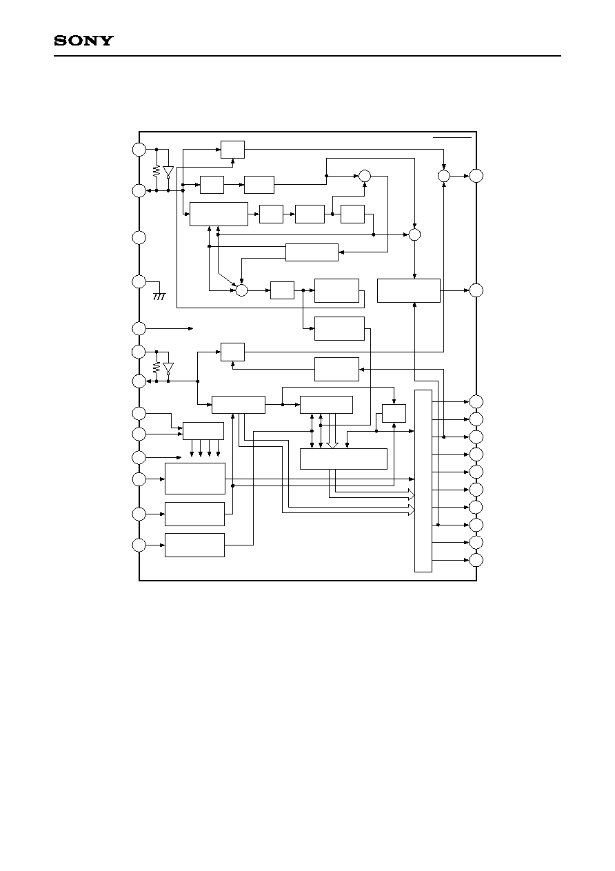
The CXD1217Q is a synchronizing signal generator
for color video cameras.
Features
ñ Compatible with the respective systems, NTSC,
PALM, PAL and SECAM
ñ Output is synchronized with the clock of 910f
H
or
908f
H
ñ 25Hz offset processing by PAL system
ñ Color framing by the respective systems, NTSC,
PALM and PAL
ñ Possible external synchronization by H reset, V
reset and line alternate reset pins
Applications
Synchronizing signal generator for color video
cameras
Structure
Silicon gate CMOS IC
Absolute Maximum Ratings (Ta = 25¯C)
ñ Supply voltage
V
DD
V
SS
Ù 0.5 to +7.0
V
ñ Input voltage
V
I
V
SS
Ù 0.5 to V
DD
+ 0.5
V
ñ Output voltage
V
O
V
SS
Ù 0.5 to V
DD
+ 0.5
V
ñ Operating temperature
Topr
Ù20 to +75
¯C
ñ Storage temperature
Tstg
Ù55 to +150
¯C
Recommended Operating Conditions
ñ Supply voltage
V
DD
4.5 to 5.5
V
ñ Operating temperature
Topr
Ù20 to +75
¯C
Ù 1 Ù
E90806A79-PS
Sony reserves the right to change products and specifications without prior notice. This information does not convey any license by
any implication or otherwise under any patents or other right. Application circuits shown, if any, are typical examples illustrating the
operation of the devices. Sony cannot assume responsibility for any problems arising out of the use of these circuits.
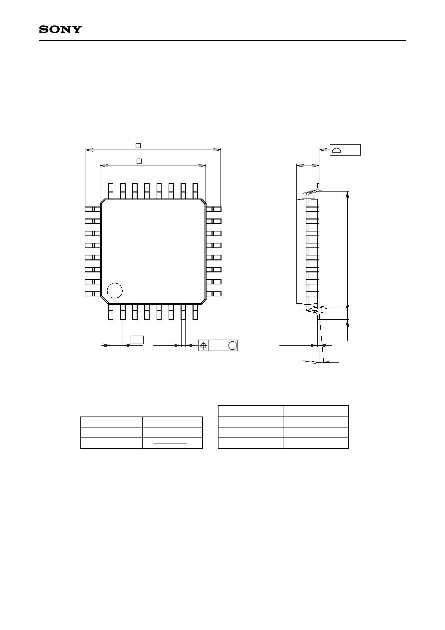
CXD1217Q
32 pin QFP (Plastic)
Ù 2 Ù
CXD1217Q
2
3
4
5
6
7
12
14
19
20
21
22
24
26
28
V
DD
OVD
OHD
OLALT
OBLK
OFLD
OSYNC
OBF/COLB
OFLD1
TEST
O2FH
OSC
EXT
MODE1
MODE2
HCOMOUT
CLOUT
CLIN
OFH
V
SS
10
4fscIN
4fscOUT
1/4
1/9
1/101
f
H
CLOCK
ELIMINATION
1/7
1/81
1/2
2f
H
PAL
PALM
f
H
PAL
PALM
1/4
SC
RESET
PAL
PALM
fv/2
f
H
1/625
1/525
PAL
1/625, 1/525
fv/8
INT-NTSC
INT-
NTSC
SC
RESET
1/4
1/454, 1/455
1/625, 1/525
2f
H
FIELD 1
RESET
1/2
O
U
T
P
U
T
F
.
F
.
VRI
VERTICAL
RESET
23
HRI
HORIZONTAL
RESET
LINE
ALTERNATE
RESET
15
LALTRI
DECODE
f
H
Note) Pin 17 output is (a) a signal based on Pin 24 in INT mode at NTSC.
(b) each signal is based on Pin 8 in other modes.
PHASE
COMPARISON
COMPOSITE SIGNAL
CONTROL F.F.
13
18
29
17
30
31
8
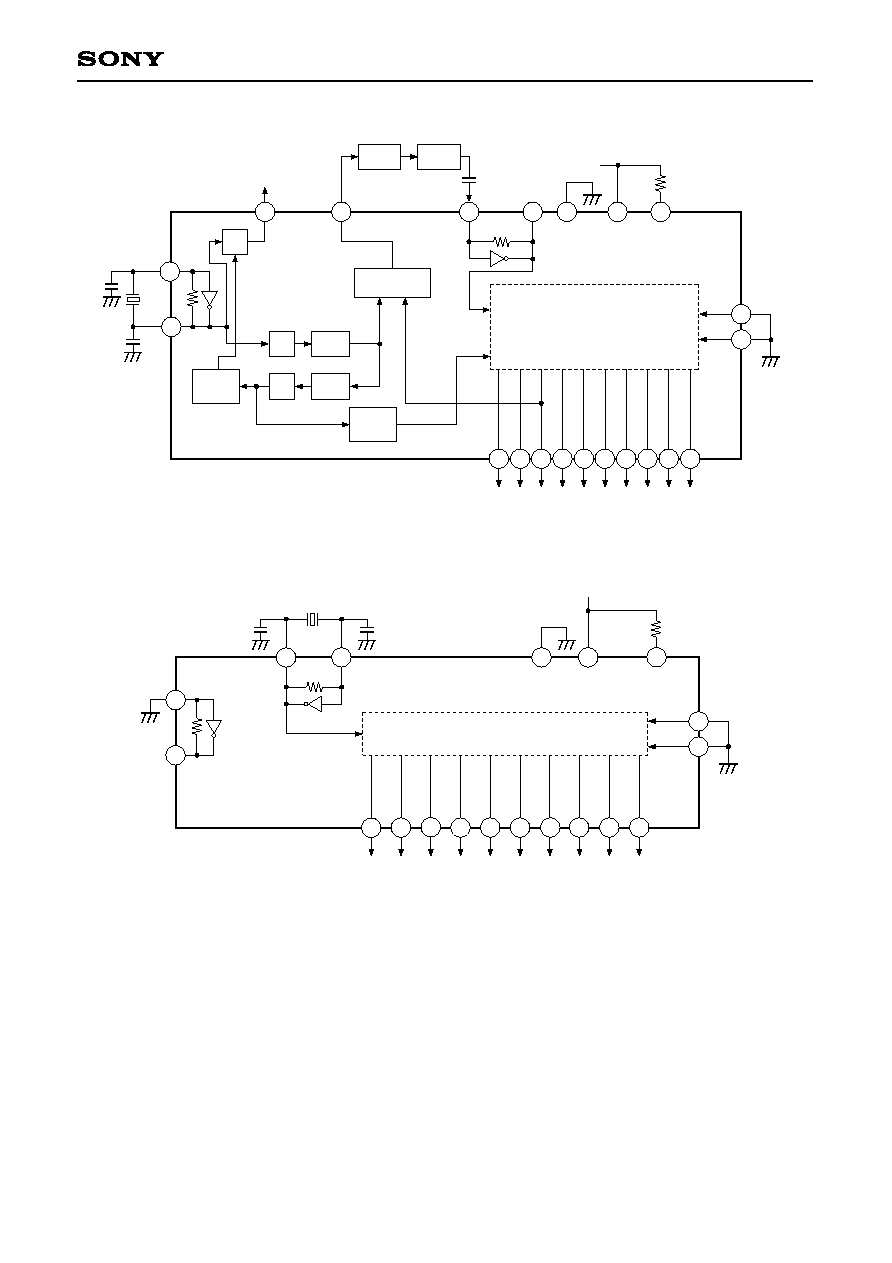
Block Diagram and Pin Configuration

Ù 3 Ù
CXD1217Q
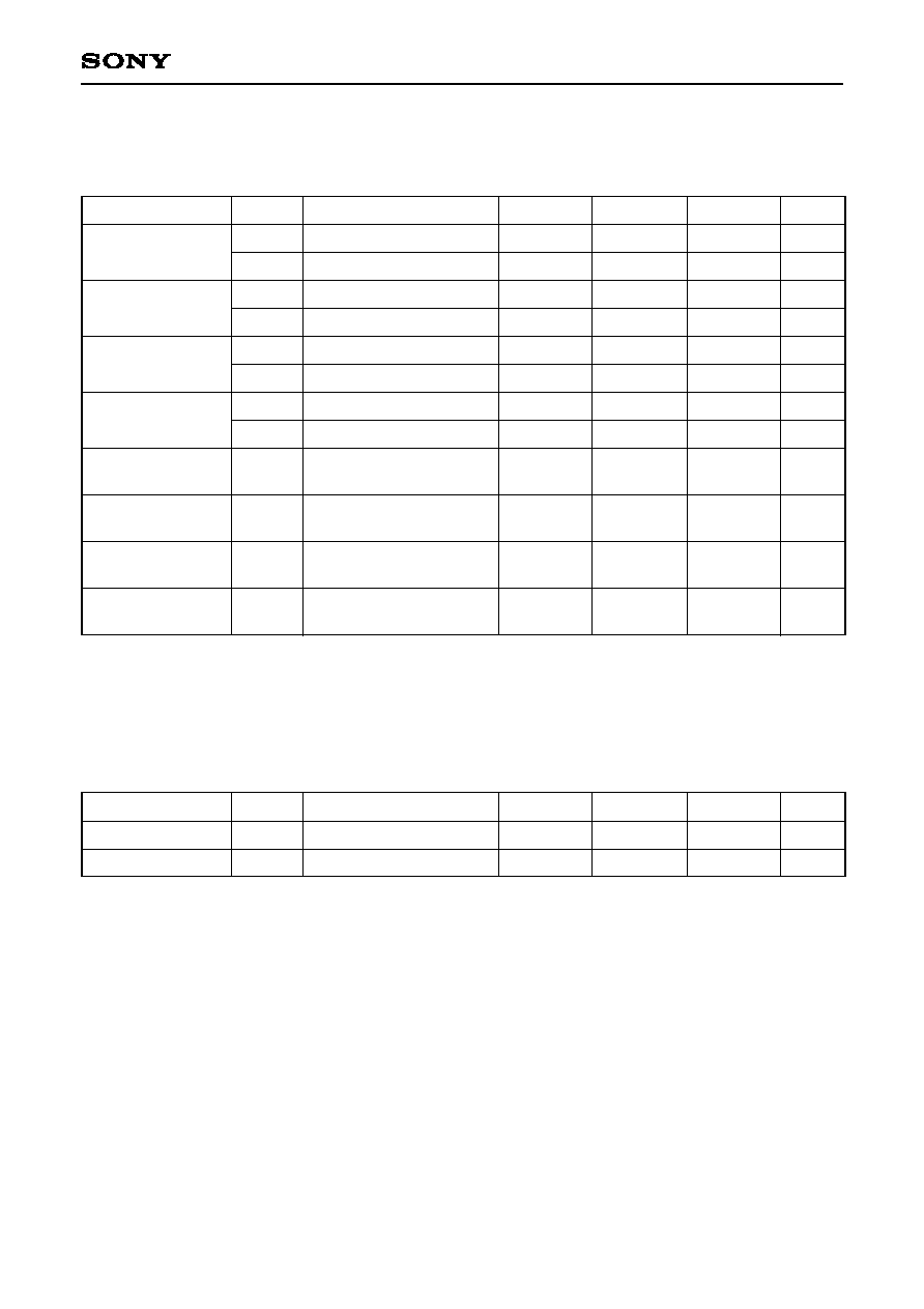
Pin Description
Pin No.
Symbol
I/O
Description
Composite sync output
Even and Odd output
Composite blanking output
Line alternate output
Horizontal drive output
4fsc output
4fsc input
Vertical drive output
GND pin
Line alternate reset input
Test input
2f
H
output (Double the frequency of Pin 27)
Sub carrier output
Internal and external synchronizing modes switchover
L: Internal synchronization H: External synchronization
System selecting input 1
System selecting input 2
Horizontal reset input
Phase comparator output
Clock output
Clock input
Horizontal frequency output
Power supply pin
Vertical reset signal
First field output
Burst flag/color blanking output
1
2
3
4
5
6
7
8
9
10
11
12
13
14
15
16
17
18
19
20
21
22
23
24
25
26
27
28
29
30
31
32
--
O
O
O
O
O
O
I
--
O
--
--
I
I
O
--
O
I
I
I
I
O
O
I
--
O
--
--
I
O
O
--
NC
OSYNC
OFLD
OBLK
OLALT
OHD
4fscOUT
4fscIN
NC
OVD
NC
V
SS
LALTRI
TEST
O2FH
NC
OSC
EXT
MODE1
MODE2
HRI
HCOMOUT
CLOUT
CLIN
NC
OFH
NC
V
DD
VRI
OFLD1
OBF/COLB
NC
Ù 4 Ù
CXD1217Q
Electrical Characteristics
DC characteristics
(V
DD
= 5V Ý 10%, V
SS
= 0V, Topr = Ù20 to +75¯C)
Item
Output voltage 1
Output voltage 2
1
Output voltage 3
2
Input voltage
Input current
3
(Pull-down pin)
Output leak
current
1
Power current
supply
Feedback
resistance
4
Symbol
Conditions
I
OH
= Ù2mA
I
OL
= 4mA
I
OH
= Ù4mA
I
OL
= 4mA
I
OH
= Ù4mA
I
OL
= 8mA
V
IH
= V
DD
At high impedance
At output pin in no-load
V
DD
= 5V
Min.
V
DD
Ù 0.5
V
SS
V
DD
Ù 0.5
V
SS
V
DD
/2
0.7V
DD
20
250k
50
Ý30
8
V
DD
0.4
V
DD
0.4
V
DD
/2
0.3V
DD
120
2.5M
V
V
V
V
V
V
V
V
çA
nA
mA
Typ.
Max.
Unit
Item
Input pin
Output pin
Symbol
C
IN
C
OUT
Conditions
Min.
--
--
--
--
9
11
pF
pF
Typ.
Max.
Unit
1
HCOMOUT pin
2
4fscOUT and CLOUT pins
3
LALTRI, TEST, EXT, MODE1 and MODE2 pins
4
4fscOUT, 4fscIN, CLOUT and CLIN pins
I/O capacitance
(V
DD
= V
I
= 0V, f
M
= 1MHz)
V
OH
V
OL
V
OH
V
OL
V
OH
V
OL
V
IH
V
IL
I
IH
I
LZ
I
DD
R
FB

Ù 5 Ù
CXD1217Q
Description of Operation (See Block Diagram.)
The CXD1217 is applicable to four systems; namely, NTSC, PAL, PALM and SECAM. In order to realize them,
the following relative equations of Sub-carrier (4fsclN) and Clock (CLIN) are adopted .
As it is obvious from the above equations, the 4fsc and clock frequency do not coincide with each other in the
PAL and PALM. Therefore matching of the clock frequency is carried out by providing PLL.
1 . MODE specified input
The CXD1217 provides four inputs to specify the respective modes.
EXT input: Set this pin to V
DD
side, and it becomes into external synchronizing mode. At this time, the
counters in connection with the PLL Ioop as shown in the upper part of the block diagram
become into stand still state.
MODE1 and MODE2 inputs: These are inputs for the system selection.
TEST input: An input to be used to measure IC. This input is normally kept opened.
(Because it is dropped internally to Vss with MOS resistance.)
2. Reset operation
The CXD1217 has three reset inputs ; namely, HRI, VRI, LALTRI, and it works to perform reset operation
when it detects falling edge. These three inputs are so designed as to take in synchronization with the IC
internal clock. Therefore, it is a prerequisite that both systems should have clock frequencies that are matched
as a reset operation to each other (GEN Iocked).
ñ H reset (HRI input)
When the HRI input is continuous with H synchronization, resetting is activated with the initial falling edge,
and for the subsequent edges they do not have to be reset unless they are deviated more than 2-bit (140ns)
against the initial edge in the internal clock. That is, if the jitter of HRI input is less than 140ns, it is absorbed.
The minimum resetting pulse width is over 0.3çs.
The phase to be reset is the advanced point of 6.3 to 6.37çs (= 90 to 91-bit
æ
70ns) than the HRI input as
shown in the diagram below.
Reset
6.3 to 6.37 [çs]
HRI input
CXD1217
HD OUT output
NTSC
PAL
PALM
SECAM
4fsc = 910f
H
4fsc = 1135f
H
+ 2fv
4fsc = 909f
H
--
Sub carrier
Clock
910f
H
908f
H
910f
H
908f
H
MODE1
0
0
1
1
MODE2
0
1
0
1
System
NTSC
SECAM
PALM
PAL
"0"
V
SS
"1"
V
DD
Ù 6 Ù
CXD1217Q
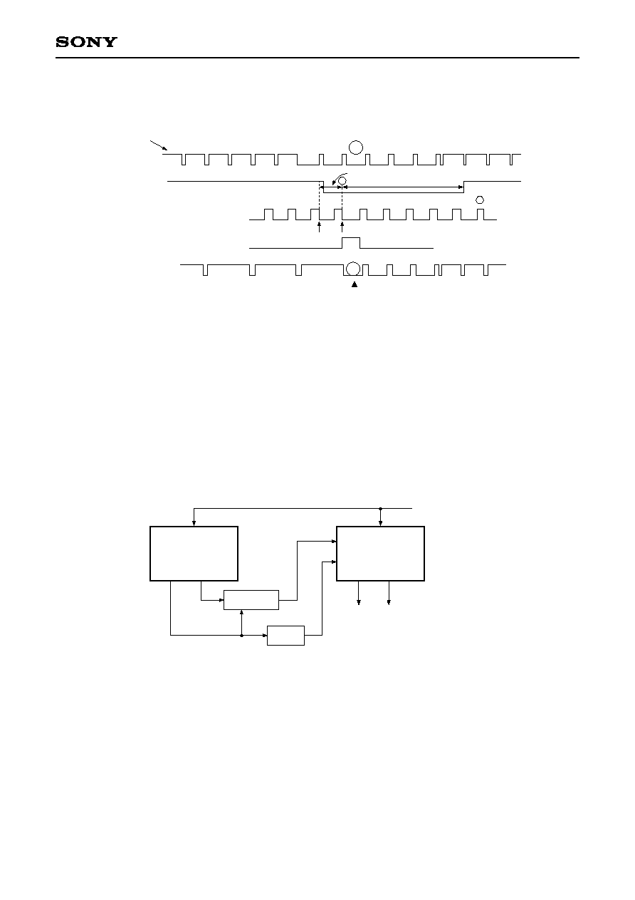
ñ V reset (VRI input)
When the VRI is input as shown in figure below, OSYNC can be reset at the same phase with the SYNC signal.
Reset State
Rising edge is to be behind from point
Falling edge permitted span
2
1
4
3
6
5
8
7
10
9
12
11
14
13
15
CXD1217 internal clock (2f
H
)
(See Timing Chart Diagram)
SYNC Signal
VRI
Counter State
V reset pulse
After reset SYNC OUT
10
9
12
11
14
13
a
a
Since the falling edge point in the diagram above (marked with
) is the boundary of reset, if the falling edge
of the VRI input traverses that point, it causes 1/2H deviation to the reset state.
Accordingly, if resetting is applied between two similar systems whose frequency are different, the V to which
resetting is applied generates jitter of 1/2H. (When the resetting is applied continuously.)
ñ LALT reset (LALTRI input)
Phase relation between LALTRI pulse polarity and 2f
H
is the same as in the case of V resetting.
Resetting operation is basically required only in the external synchronizing mode (GEN LOCK mode). However,
even in the internal synchronizing mode, it sometimes requires H and V outputs whose phases are deviated
against a certain output. In that case, it suffices to use two CXD1217s and conduct the operation as follows:
CXD1217
OHD1
OVD1
CXD1217
OHD2
OVD2
VRI2
VRI2
Clock
Shift Reg.
Delay
Clock
Output
Input
It suffices to set IC-1 and IC-2 into INT mode.
By varying the Delay and Shift Reg. of the above diagram, any phases of OHD2 and OVD2 can be provided
against the respective OHD1 and OVD1.
3. Color framing
In the case of internal synchronization in the individual NTSC, PAL and PALM systems, the phase
relationships between SYNC of the 1st field and sub-carrier are kept stable regardless of the power supply
being ON or OFF. However, as the PAL and PALM systems are comprised of PLL, the absolute values
concerning the phase according to variation of the ambient temperature drifts.
Ù 7 Ù
CXD1217Q
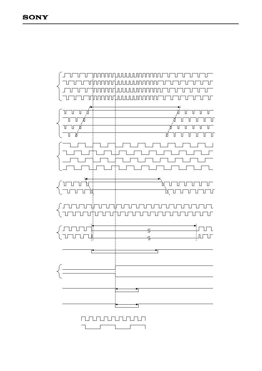
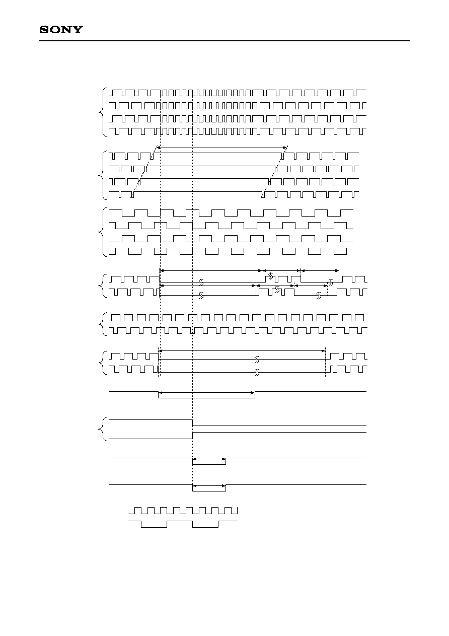
Timing Chart
Output Timing Chart Diagram
CXD1217 NTSC, PALM
Field 1
2
3
4
LALT OUT
(PALM)
ODD
Field 1
2
3
4
EVEN
ODD
EVEN
SYNC OUT
BF/COLB OUT
(PALM)
Field 1
2
3
4
12H
10H
ODD
EVEN
BF/COLB OUT
(NTSC)
ODD
EVEN
ODD
EVEN
20H
HD OUT
BLK OUT
9H
VD OUT
FLD OUT
3H
3H
ODD
EVEN
Field 1
Field 1
FLD1 OUT (fv/4)
(NTSC)
FLD1 OUT (fv/8)
(PALM)
CLIN
(NTSC)
4fscIN
(PALM)
SC OUT
Ù 8 Ù
CXD1217Q
CXD1217 PAL, SECAM
Field 4
1
2
3
LALT OUT
(PAL)
EVEN
Field 4
1
2
3
ODD
EVEN
ODD
SYNC OUT
BF/COLB OUT
(PAL)
Field 4
1
2
3
10H
9H
EVEN
ODD
BF/COLB OUT
(SECAM)
EVEN
ODD
EVEN
ODD
25H
HD OUT
BLK OUT
7.5H
OVD
FLD OUT
2.5H
2.5H
EVEN
ODD
FLD1 OUT (fv/8)
(PAL)
FLD1 OUT (fv/4)
(SECAM)
4fscIN
(PAL)
SC OUT
9H
7H
8.5H
9H
7H
Ù 9 Ù
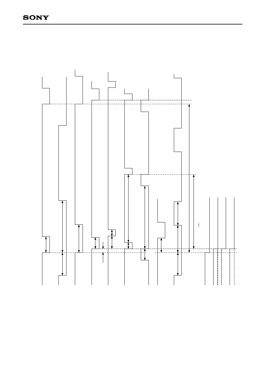
CXD1217Q
CXD1217 f
H
H
D
/
C
B
L
K
P
1
3
9
N
1
4
0
P
3
1
5
N
3
1
5
P
9
6
N
9
6
P
1
6
9
N
1
5
4
P
6
6
N
6
8
P
2
2
N
2
2
P
3
2
N
3
6
P
7
8
N
7
6
P
3
4
N
3
2
P
6
6
N
6
8
P
4
2
0
N
4
2
3
P
3
8
8
N
3
8
7
P
1
4
0
N
1
4
1
P
9
0
N
9
0
P
1
6
9
N
1
6
9
P
1
4
5
N
1
4
5
P
4
5
4
N
4
5
5
1
2
H
P
9
0
8
N
9
1
0
H
P
:
P
A
L
S
E
C
A
M
N
:
N
T
S
C
P
A
L
M
N
u
m
e
r
i
c
a
l
f
i
g
u
r
e
s
s
h
o
w
n
u
m
b
e
r
o
f
c
l
o
c
k
s
f
H
H
B
L
K
H
S
Y
N
C
B
F
E
Q
V
S
Y
N
C
H
.
R
.
2
f
H
V
D
F
L
D
F
L
D
1
L
A
L
T
(
I
n
t
e
r
n
a
l
c
l
o
c
k
)
Ù 10 Ù
CXD1217Q
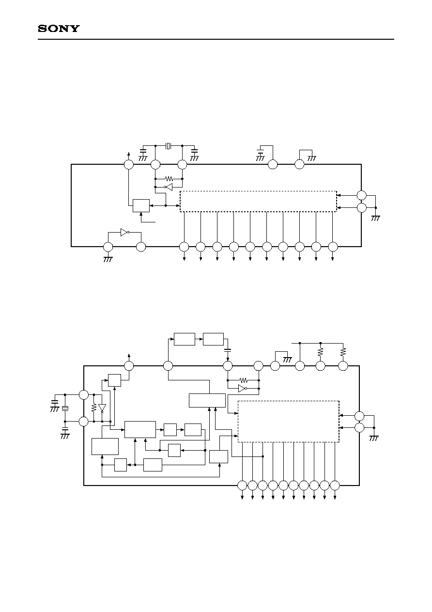
Application Circuit
Basic connection in individual systems
Basic connection in individual systems at internal synchronization mode (EXT input = "0") is as follows. See
waveform diagram for each output.
VRI
OSC
HRI
CLOUT
CLIN
O
V
D
O
H
D
O
L
A
L
T
O
B
L
K
O
F
L
D
O
S
Y
N
C
O
B
F
/
C
O
L
B
O
F
L
D
1
O
2
F
H
O
F
H
4fscIN
4fscOUT
1/4
V
DD
28
V
SS
V
DD
14.318MHz ( = 910f
H
)
Synthesizer
OLALT
24
2
3
4
6
7
8
17
23
26
12
10
21
29
30
31
13
15
ñ NTSC
H/2 is output for LALT OUT even in NTSC mode.
MODE1, MODE2, EXT, TEST and LALTRI pins can be kept open.
(If noise annoys, connect to Vss by low impedance.)
MODE1 MODE2
HCOMOUT
Clock
Elimination
1/7
1/81
f
H
S. C.
Reset
1/2
1/625
1/8
Field
1/4
17.734MHz
(4fsc)
4fsc
IN
4fsc
OUT
O
V
D
O
H
D
O
L
A
L
T
O
B
L
K
O
F
L
D
O
S
Y
N
C
O
B
F
/
C
O
L
B
O
F
L
D
1
O
2
F
H
O
F
H
23
VRI
HRI
OSC
CLOUT
CLIN
V
DD
10k
10k
V
DD
V
SS
L. P. F
VCO
Synthesizer
14.187MHz ( = 908f
H
)
Phase
Comparison
f'
H
24
2
3
4
6
7
8
17
19
26
28
12
10
21
22
29
30
31 13
15
20
ñ PAL
Inverter of CLIN or CLOUT pins are usable as VCO.
Application circuits shown are typical examples illustrating the operation of the devices. Sony cannot assume responsibility for
any problems arising out of the use of these circuits or for any infringement of third party patent and other right due to same.
Ù 11 Ù
CXD1217Q
24
MODE1
HCOMOUT
Phase
Comparison
1/9
1/101
f
H
1/525
1/8
Field
1
1/4
14.302MHz
(4fsc)
4fsc
IN
4fsc
OUT
O
V
D
O
H
D
O
L
A
L
T
O
B
L
K
O
F
L
D
O
S
Y
N
C
O
B
F
/
C
O
L
B
O
F
L
D
1
O
2
F
H
O
F
H
2
3
4
6
7
8
17
23
VRI
HRI
19
26
OSC
CLOUT
CLIN
V
DD
28
10k
V
DD
V
SS
L. P. F
VCO
Synthesizer
14.318MHz ( = 910f
H
)
S. C.
Reset
f'
H
12
10
21
22
29
30
31 13
15
ñ PALM
Internal inverter is usable as VCO.
10k
V
DD
23
VRI
HRI
CLOUT
CLIN
O
V
D
O
H
D
O
L
A
L
T
O
B
L
K
O
F
L
D
O
S
Y
N
C
O
B
F
/
C
O
L
B
O
F
L
D
1
O
2
F
H
O
F
H
V
DD
V
SS
14.187MHz ( = 908f
H
)
2
3
4
7
Synthesizer
MODE2
10
4fscIN
8
26
28
6
15
13
31
30
20
21
29
12
24
ñ SECAM
COLB is output to BF/COLB OUT pin.
S
DR
and S
DB
are formed in PLL using 908f
H
.
Application circuits shown are typical examples illustrating the operation of the devices. Sony cannot assume responsibility for
any problems arising out of the use of these circuits or for any infringement of third party patent and other right due to same.
Ù 12 Ù
CXD1217Q
Package Outline
Unit: mm
SONY CODE
EIAJ CODE
JEDEC CODE
PACKAGE MATERIAL
LEAD TREATMENT
LEAD MATERIAL
PACKAGE MASS
EPOXY RESIN
SOLDER PLATING
42 ALLOY
32PIN QFP (PLASTIC)
9.0 Ý 0.2
7.0 Ù 0.1
1.5 Ù 0.15
(
8
.
0
)
0.1 Ù 0.1
+ 0.2
+ 0.35
+ 0.3
0
.
5
0
0.127 Ù 0.05
+ 0.1
0¯ to 10¯
0.8
0.3 Ù 0.1
+ 0.15
1
8
9
32
16
17
24
25
M
0.24
0.2g
QFP-32P-L01
QFP032-P-0707
0.1