1
E01Y22A2Z-PS
Sony reserves the right to change products and specifications without prior notice. This information does not convey any license by
any implication or otherwise under any patents or other right. Application circuits shown, if any, are typical examples illustrating the
operation of the devices. Sony cannot assume responsibility for any problems arising out of the use of these circuits.
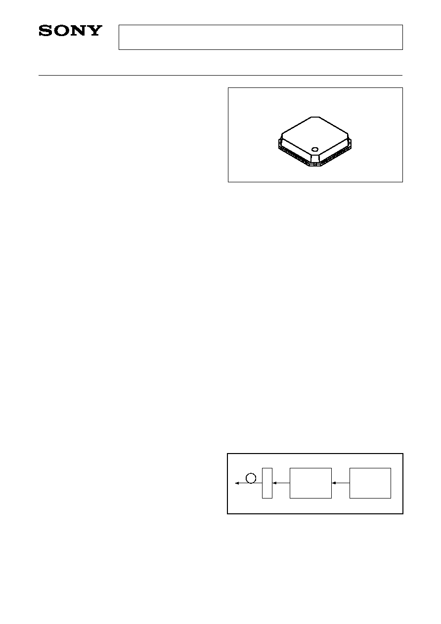
CXB1828ER
32 pin VQFN (Plastic)
2.5Gbps Laser Diode Driver
Description
The CXB1828ER is a high-speed monolithic laser
diode driver. This IC can drive the data rate of 2.5Gbps
and the modulation current of up to 50mA. The bias
current of up to 50mA can be supplied and it is
controlled by the built-in APC (automatic power
control). The modulation current and bias current are
designed to be linearly controlled by the voltage input
to the control pin.
This IC has a built-in DFF, and through mode or DFF
mode can be selected. In through mode the signal
goes as it is, and in DFF mode the input signal is
retimed by the external clock. The data input pin and
the clock input pin can accept the differential input of
PECL and CML, and the 50
termination resistors are
provided in the IC.
The shutdown function which shuts down the
modulation current and bias current, the activity error
detect circuit which detects that the signal has no
input, and the alarm output power-on reset circuit.
Furthermore, the duty cycle control circuit which
corrects the modulation output signal duty is
included in this IC.
The CXB1828ER employs the 4.8mm
×
4.8mm
of 32-pin plastic package, contributing to the
miniaturization of the optical mode.
Features
· Direct laser diode drive
· Maximum data rate of 2.5Gbps
· Power-on reset function
· Automatic power control (APC) for bias current
· Alarm function and shutdown function
· Differential PECL and CML inputs or AC coupled
input
· Internal duty cycle correction circuit
· Activity error detector function for laser safety
· Typical rise time is 80ps.
· Built-in 50
input termination resistor
· Compact package size: 4.8mm
×
4.8mm
· Single +3.3V supply voltage
Applications
· Gigabit ethernet: 1.25Gbps
· SONET/SDH: 622Mbps, 2.5Gbps
Sony
CXB1828ER
Sony
SerDes
Laser Diode
Transmit Path
Typical Transmit Block Diagram
Absolute Maximum Ratings
· Supply voltage
Vcc V
EE
0.3 to +6.0
V
· Data and clock input voltage difference
|V
D
V
DN
|
2.5
V
· Bias output current
100
mA
· Modulation output current
100
mA
· Storage temperature
Tstg
65 to +150
°C
Recommended Operating Conditions
· Supply voltage
Vcc V
EE
3.14 to 3.46
V
· Operating ambient temperature
Ta
40 to +85
°C
Important Notes
The IC requires SLOW turning power on and off.
See Vcc rise and fall time in AC characteristics.
Electrostatic Strength
This IC has a very sensitive electrostatic strength,
so care should be taken for handling.

2
CXB1828ER
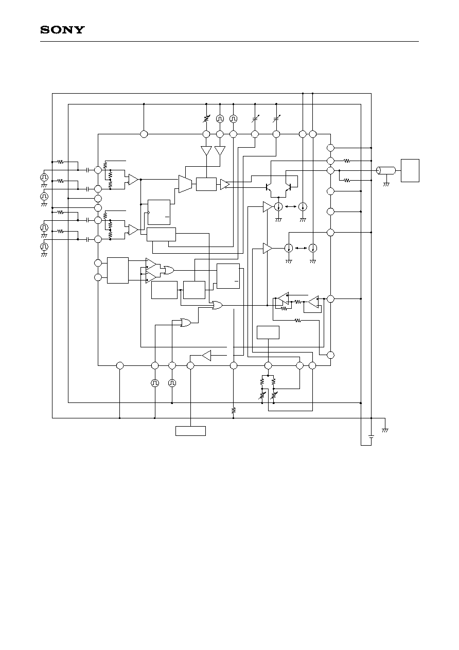
Block Diagram
50
10k
Vcc 1.4V
50
50
10k
Vcc 1.4V
50
50:1
QB
BIAS
BIAS_SET
OP_OUT
OP_IN
VREF
MOD_SET
RREF
Q
Duty
Control
Activity Error
Detector
Vcc
Voltage Error
Det.
Time
Stretcher
Vref Gen.
High
Low
MUX
1
D
Q
Q
1.8V
0.3V
0
kill
50:1
4k
15k
Vref 1.1V
60k
kill
S
R
Q
Q
Vref
Gen 1.9V
to Modulation/Bias Control
THR
UMODE
DUTY
MOD_MON
BIAS_MON
DIN
DINB
AED_CAP
AED_DISABLE
WCVH
WCVL
TIME_CAP
ALARM
SHUTDOWNB
SHUTDOWN
CKIN
CKINB
Pin Assignment
25
26
27
28
29
30
31
32
24 23 22 21 20 19 18 17
DIN
V
EE
2
DUTY
THR
UMODE
AED_DISABLE
TIME_CAP
AED_CAP
MOD_MON
BIAS_MON
1
2
3
4
5
6
7
8
V
CC
2
SHUTDO
WNB
SHUTDO
WN
ALARM
RREF
VREF
MOD_SET
BIAS_SET
DINB
V
EE
1
V
CC
1
CKIN
CKINB
WCVH
WCVL
16
15
14
13
12
11
10
9
V
CC
O
QB
Q
V
EE
O1
V
EE
O2
BIAS
OP_IN
OP_OUT

3
CXB1828ER
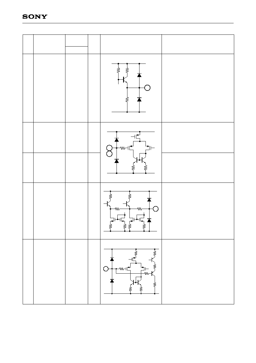
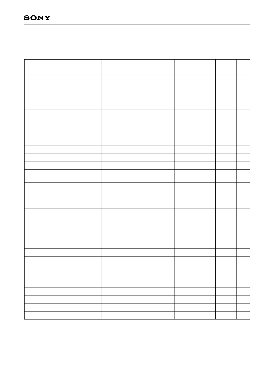
Pin Description
Pin
No.
Symbol
Typical pin
voltage (V)
DC
Description
I/O
Equivalent circuit
2
3
Vcc2
10k
10k
V
EE
2
4
Vcc2
V
EE
2
5
Vcc2
V
EE
2
1
Vcc2
3.3
Positive power supply.
2
SHUTDOWNB
0 or Vcc
I
TTL input.
The modulation current and bias
current is shut down by inputting
the Low voltage to this pin. High
level when open.
3
SHUTDOWN
0 or Vcc
TTL input.
The modulation current and bias
current is shut down by inputting
the High voltage to this pin. High
level when left open.
4
ALARM
O
TTL output.
High when the abnomality is
detected from the OP_IN pin
voltage. The abnormal voltage of
OP_IN is Vop < 0.3V or Vop > 1.8V.
5
RREF
Connect an external resistor of
18k
between this pin and Vcc.
I
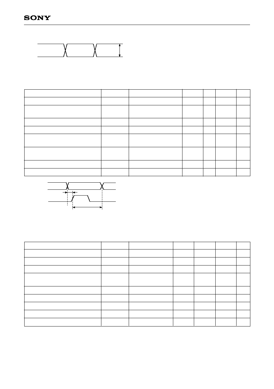
4
CXB1828ER
Pin
No.
Symbol
Typical pin
voltage (V)
DC
Description
I/O
Equivalent circuit
6
Vcc2
V
EE
2
26.4K
7
8
Vcc2
V
EE
2
9
Vcc2
4k
V
EE
2
150k
10
Vcc2
V
EE
2
6
VREF
1.9
O
9
OP_OUT
O
7
MOD_SET
0.2 to 2.0
I
8
BIAS_SET
0.2 to 2.0
I
10
OP_IN
0.3 to 1.8
I
Reference voltage output.
GND reference 1.9V.
Internal operational amplifier
output.
Used for the bias current
automatic power control (APC).
The OP_OUT pin is connected to
the BIAS_SET pin. Connect a
0.1µF capacitor between this pin
and GND.
Modulation current control.
The modulation current is
controlled by this pin voltage.
Bias current control.
The bias current is controlled by
the voltage of this pin.
The internal operational amplifier
input for the bias current automatic
power control (APC).

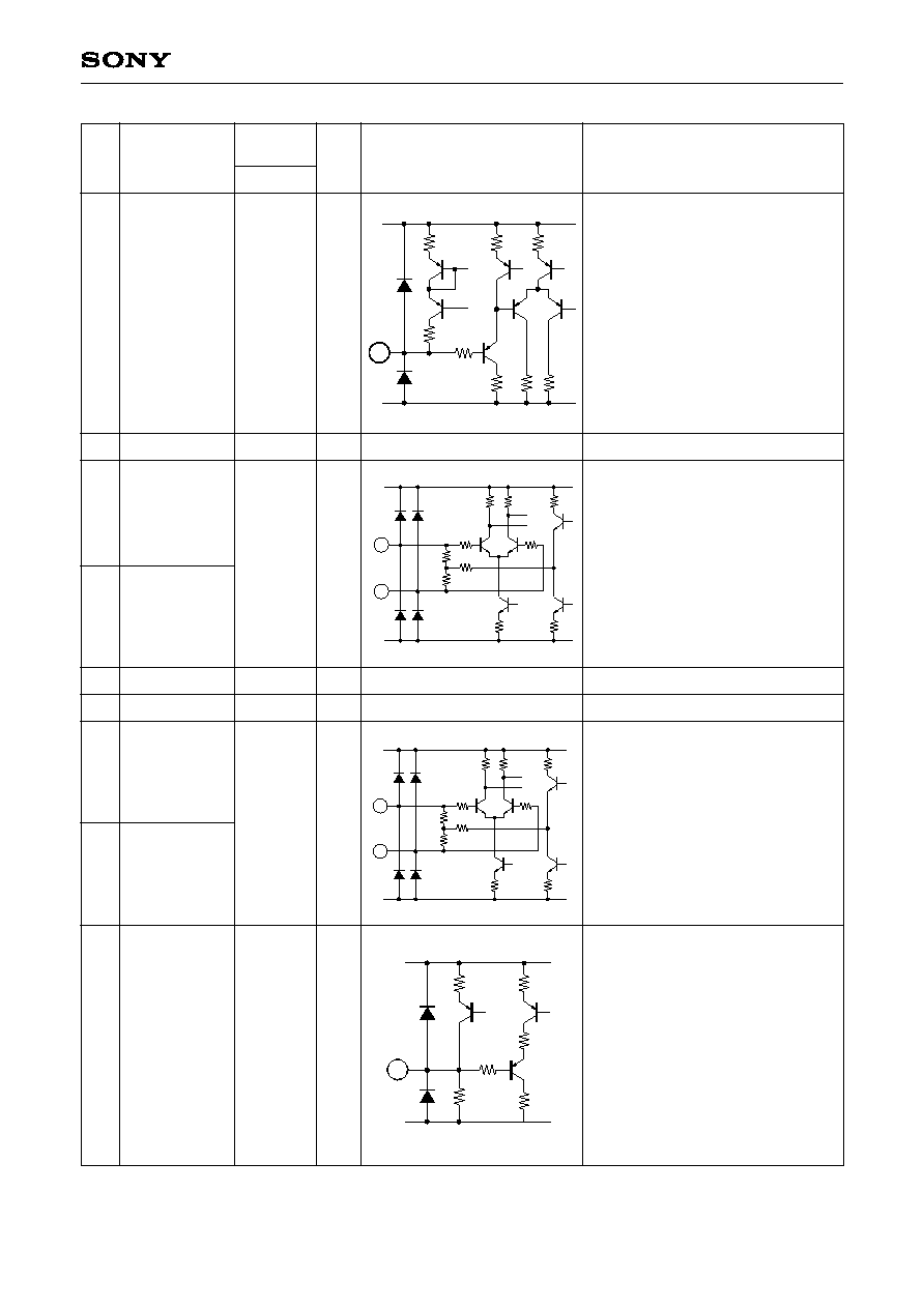
5
CXB1828ER
Pin
No.
Symbol
Typical pin
voltage (V)
DC
Description
I/O
Equivalent circuit
11
V
EE
O2
V
CC
1
Current
Source
14
15
V
EE
O1
V
EE
O1
V
CC
O
Current
Source
17
18
V
EE
1 (MOD_MON)
V
EE
O2 (BIAS_MON)
V
CC
1
Current
Source
11
BIAS
O
Laser bias current output.
12
V
EE
O2
0
Negative power supply for the
modulation and bias output.
13
V
EE
O1
0
Negative power supply for the
modulation output.
14
Q
O
Laser modulation current output.
Open collector output.
15
QB
O
Complementary current output.
Connect the laser diode not to this
pin, but to the Q pin.
16
VccO
3.3
Positive power supply for the
modulation output.
17
BIAS_MON
O
Bias current monitor.
1/50 of the bias current flows
to this pin. This pin is connected to
Vcc either through a resistor 1k
or directly.
18
MOD_MON
O
Modulation current monitor.
1/50 of the modulation current
flows to this pin. This pin is
connected to Vcc either through a
resistor 1k
or directly.
6
CXB1828ER
Pin
No.
Symbol
Typical pin
voltage (V)
DC
Description
I/O
Equivalent circuit
19
Vcc2
30pF
500
V
EE
2
20
Vcc2
30pF
500
V
EE
2
21
Vcc2
10k
10k
V
EE
2
22
Vcc2
10k
10k
V
EE
2
19
AED_CAP
Capacitor connection for the
activity error detector. If the active
detector function is not required,
this pin can be left open.
When a capacitor is connected
between the AED_CAP pin and
Vcc, the time till the error is
detected can be extended.
20
TIME_CAP
Capacitor connection for the alarm
power-on reset.
The period of the power-on reset
time is controlled by a capacitor
(recommended value is 0.01µF)
connected between the TIME_CAP
pin and GND.
If the ALARM function is not
required, this pin can be left open.
21
AED_DISABLE
I
TTL input.
This pin controls the activity error
detector circuit.
When High (open or connected to
Vcc), the activity error detector
function is disabled. When Low
(connected to GND), the activity
error detector function is enabled.
22
THRUMODE
I
TTL input.
When High (open or connected to
Vcc), the input data goes not
through the D flip-flop.
When Low (connected to GND),
the serial input data goes through
the D flip-flop within the chip.
7
CXB1828ER
Pin
No.
Symbol
Typical pin
voltage (V)
DC
Description
I/O
Equivalent circuit
Vcc1
23
300
300
V
EE
1
25
26
Vcc1
50
50
V
EE
1
10k
29
30
Vcc1
50
50
V
EE
1
10k
31
Vcc2
36k
V
EE
2
23
DUTY
Resistor connection for the duty
cycle control.
When an external resistor is
connected between the DUTY pin
and GND, the modulation pulse
width can be expanded.
24
V
EE
2
0
Negative power supply.
25
DIN
PECL
or
CML
I
Differential PECL and CML data
inputs.
These two inputs are internally
connected by 100
and biased by
10k
to Vcc 1.4V.
26
DINB
27
V
EE
1
0
Negative power supply.
28
Vcc1
3.3
Positive power supply.
29
CKIN
PECL
or
CML
I
Differential PECL and CML clock
inputs.
These two inputs are internally
connected by 10k
and biased by
10k
to Vcc 1.4V.
30
CKINB
31
WCVH
1.8
Window comparator's higher
threshold voltage for ALARM.
The default high alarm assert
voltage for the comparator is 1.8V.

8
CXB1828ER
Pin
No.
Symbol
Typical pin
voltage (V)
DC
Description
I/O
Equivalent circuit
31
Vcc2
6k
8k
V
EE
2
32
WCVL
0.3
Window comparator's lower
threshold voltage for ALARM.
The default low alarm assert
voltage for the comparator is 0.3V.
9
CXB1828ER
Electrical Characteristics
DC Characteristics
(Vcc V
EE
= 3.14 to 3.46V, Ta = 40 to +85°C)
DC power supply voltage
Supply current
(DATA THRU MODE)
Supply current (D-FF MODE)
Maximum modulation output
current
Minimum modulation output
current
Modulation output voltage range
Maximum bias output current
Minimum bias output current
Bias output voltage range
Modulation shutdown current
Bias shutdown current
DIN, CKIN input High voltage
(PECL)
DIN, CKIN input Low voltage
(PECL)
DIN, CKIN differential input
voltage (CML)
Internal resistance between
DIN and DINB, CKIN and CKINB
Internal input reference voltage at
DIN, DINB, CKIN, CKINB
TTL input High voltage
TTL input Low voltage
TTL input current High
TTL input current Low
ALARM output High voltage
ALARM output Low voltage
VREF output voltage
WCVH output voltage
WCVL output voltage
Vcc voltage error detect voltage
Item
V
DC
ICC_THRU
ICC_DFF
I
QMAX
I
QMIN
V
Q
I
BMAX
I
BMIN
V
B
I
QSHD
I
BSHD
V
EIH
V
EIL
V
IN
R
DI
, R
CK
V
EIR
V
TIH
V
TIL
I
TIH
I
TIL
V
TOH
V
TOL
V
REF
V
WH
V
WL
Vcc_err
Symbol
Vcc V
EE
I
Q
= 0mA, I
B
= 0mA
I
Q
= 0mA, I
B
= 0mA
1
1
2
Iin = 0.4mA
Iin = 2.0mA
Iout = 0 to 500µA
Open voltage
Open voltage
Conditions
3.14
50
Vcc 2
50
Vcc 2
Vcc
1.17
Vcc
1.84
400
70
2.0
0.3
250
2.4
0
1.80
1.70
0.28
2.59
Min.
3.46
84
88
7
Vcc
3
Vcc
100
100
Vcc
0.81
Vcc
1.48
2000
130
Vcc +
0.3
0.8
5
Vcc
0.5
2.05
2.05
0.37
3.08
Max.
3.3
62
65
Vcc
1.37
Typ.
V
mA
mA
mA
mA
V
mA
mA
V
µA
µA
V
V
mVp-p
V
V
V
µA
µA
V
V
V
V
V
V
Unit
1
Since the internal input reference voltage may become lower than the Low level of ECL, input the signal
into DIN and CKIN by AC coupling at the time of a single phase input.
10
CXB1828ER
AC Characteristics
(Vcc V
EE
= 3.14 to 3.46V, Ta = 40 to +85°C)
Maximum data rate
Maximum variable High pulse width
by duty cycle control
Rise time (20 to 80%)
Fall time (80 to 20%)
DIN CKIN setup time
DIN CKIN hold time
Vcc rise time
Vcc fall time
Item
fdmax
t
delay
t
r
t
f
t
s
t
h
t
vccr
t
vccf
Symbol
Data rate = 2.5Gbps
I
Q
= 50mA, RL = 25
I
Q
= 50mA, RL = 25
Rise and fall time of
input = 130ps
3
Rise and fall time of
input = 130ps
3
10 to 90%
90 to 10%
Conditions
2.488
100
30
50
5
5
Min.
Max.
80
90
Typ.
Gbps
ps
ps
ps
ps
ps
ms
ms
Unit
DC/AC Characteristics for the APC Circuit
(Vcc V
EE
= 3.14 to 3.46V, Ta = 40 to +85°C)
OP_IN input voltage range
OP_OUT output maximum voltage
OP_OUT output minimum voltage
Minimum OP_OUT output voltage
at shutdown condition
OP_IN input current
OP_OUT output source current
OP_OUT output sink current
APC operational amplifier gain
Monitor photodiode current range
Item
V
I_OP
V
O_OPMAX
V
O_OPMIN
V
O_OPSDN
I
I_OP
I
O_OPSORC
I
O_OPSINK
A
V
I
MPD
Symbol
Conditions
0.2
2.0
10
Min.
2.0
0.2
1
4
4
1000
Max.
Fig. 15
12
Typ.
V
V
V
V
µA
µA
µA
dB
µA
Unit
2
V
IN
3
Setup time, Hold time
Min.: 200mV for each input
Max.: 1000mV for each input
th
DIN
CKIN
ts

11
CXB1828ER
Functional Block Description
APC (Automatic power control)
The APC loop consists of the laser driver and APC operational amplifier. The APC operational amplifier is
configured as an inverting integrator. It is the input voltage that is derived from the monitor current by the
monitor photodiode and an external resistor R
PD
to OP_IN.
The input voltage is inverted and the output from OP_OUT. The bias current is controlled by inputting the
output to the BIAS_SET pin. The bias current is set by R
PD
. A capacitor C
PD
with a value of 1000pF works for
stability and reduces the noise. Use C
APC
(recommended value 0.1µF) between the OP_OUT pin and V
EE
.
C
APC
controls the rapid rise of the OP_OUT pin when the shutdown is cancelled, and suppresses the excess
current flowing to the laser diode.
CXB1828ER
Vcc
BIAS
Q
Monitor PD
Vref_1.1V
C
PD
1000pF
R
PD
LD
OP_IN
Modulation Current
Bias Current
CXB1828ER
APC Operational Amplifier
OP_OUT
15k
60k
4k
C
APC
0.1µF
Fig.1. APC Function Block Diagram
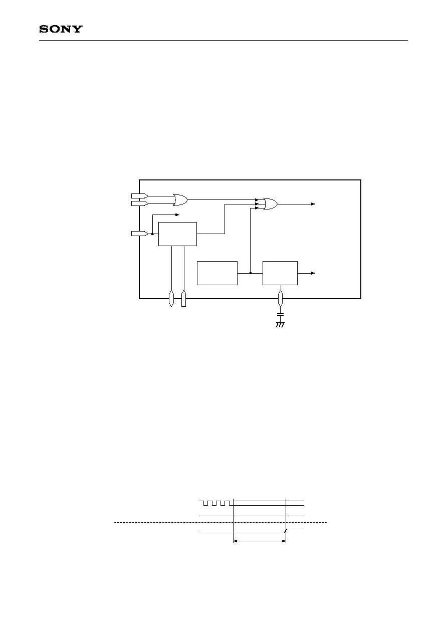
Alarm function
This circuit is for the APC operation. When the input OP_IN is provided with an excess voltage or minimal
voltage, the window comparator output goes High, and this signal is latched resulting in the output of alarm
signal. The WCVH and WCVL pin voltages are the upper and the lower threshold values of the window
comparator for ALARM. The default value of WCVH is 1.8V and that of WCVL is 0.3V. If the voltage of OP_IN is
lower than WCVL or higher than WCVH, ALARM signal is asserted High. This alarm signal returns to Low only
by the Vcc power-on reset function. Power-on reset time (T
TIME
) is set by the external capacitor put between
the TIME_CAP pin and V
EE
. (Refer to Fig. 8.) It is necessary for the alarm signal output to be Low forcibly
because the excess voltage or minimal voltage may be applied to the OP_IN pin till the APC operation completes.
The recommended value of the capacitor is 0.01µF.
Activity Error Detector
1.8V
S
R
Q
0.3V
SHUTDOWN/SHUTDOWNB
Modulation/Bias Current OFF
ALARM
Operational Amplifier for APC
Monitor PD
Window Comparator
Time
Stretcher
RS-FF
Vcc
Voltage Error
Detector
TIME_CAP
C
TIME
0.01µF
R
PD
OP_IN
Vcc > 2.9V
L
L
H
T
TIME
ALARM
ENABLE
Vcc < 2.9V
Vcc Voltage Error Detector
AED_DISABLE
SHUTDOWN
SHUTDOWNB
Modulation/Bias Current OFF
IN
OUT
APC Settling
Alarm Reset
Fig.2. Alarm Function Block Diagram
Fig.3. Timing Chart of Alarm Function
12
CXB1828ER
Data input
The PECL/CML signal is input to the data buffer at a maximum data rate of 2.5Gbps. This input pin is biased
by the reference bias voltage (Vcc 1.4V) for the AC coupling input. An on-chip 100
resistor is put between
the DIN and DINB pins. The data buffer has the frequency detector and input amplitude voltage detector for the
Activity Error Detector (AED).
Clock input
The PECL/CML clock is input to the clock buffer at a maximum data rate of 2.5GHz. This input pin is biased by
the reference bias voltage (Vcc 1.4V) for the AC coupling input. An on-chip 100
resistor is put between the
CKIN and CKINB pins.
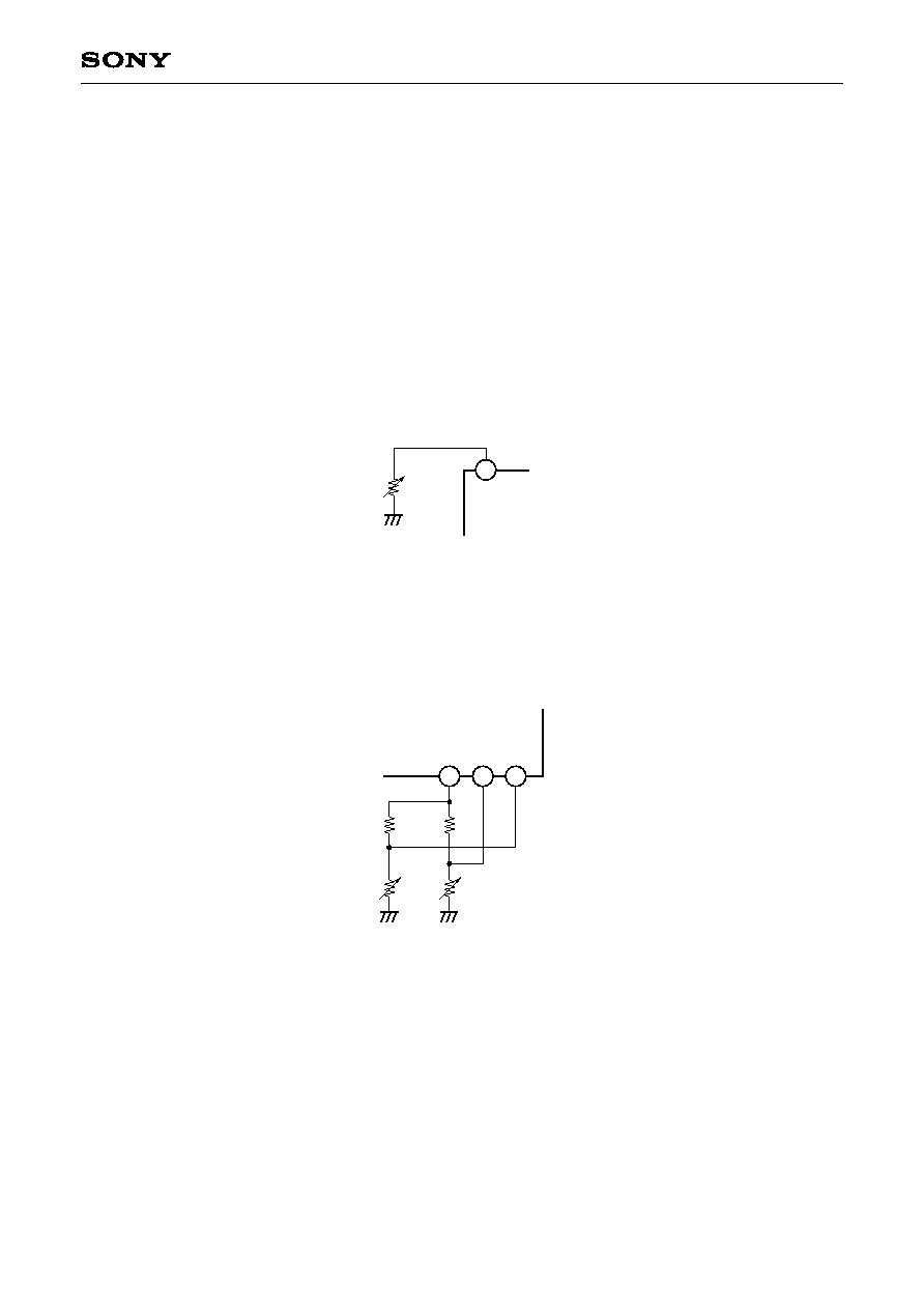
Signal duty cycle correction
The output pulse width can be extended as shown in Fig.9 by connecting an external resistor between the
DUTY pin and V
EE
, and setting its resistor value from 0
to 4k
. The output pulse width can be extended up to
100ps (min.). Short the DUTY pin to V
EE
when not want to vary the duty.
23
DUTY
0 to 4k
Fig.4. Duty Cycle Control
Bias current and modulation current control
The bias current and modulation current can be controlled linearly by the voltage input to the BIAS_SET and
MOD_SET pins as shown in Figs.10 and 11. The voltage applied to the BIAS_SET and MOD_SET pins can be
set by the external resistor between the VREF pin and V
EE
. Refer to Fig.5.
BIAS_SET
10k
R
BIAS
8
MOD_SET
7
VREF
6
R
MOD
10k
Fig.5. Modulation/Bias Control
Bias current and modulation current monitor
This circuit monitors the bias and modulation current. The BIAS_MON and the MOD_MON pins should be
connected to V
CC
either directly or through a resistor. The modulation current and monitor current are in the
rate of approximately 50:1. (Refer to Fig.12 and Fig.13.)
Thru-mode
When this pin is High or connected to Vcc, the input data goes not through the internal flip-flop. If this pin is
grounded the input data goes through the D flip-flop.
13
CXB1828ER
Shutdown function
This circuit disables the output current, that is, the bias and modulation current is turned off and used to shut
off the laser. And the voltage of OP_OUT is set to V
EE
. The function block diagram for all of the shutdown
mechanism for the circuit is shown in Fig.6. The shutdown functions when one of the following conditions is met.
1) SHUTDOWN is High.
2) SHUTDOWNB is Low.
3) The activity error detector detects an error of the DIN/DINB input signal.
4) The voltage error detector detects Vcc is below 2.59 to 3.08V.
(
The bias current may flow at approximately Vcc = 2.0V.)
SHUTDOWN
SHUTDOWNB
DIN/DINB
AED_CAP
AED_DISABLE
TIME_CAP
Input Buffer
Alarm Reset
Modulation/Bias Current OFF,
The voltage of OP_OUT is set to V
EE
.
Activity Error
Detector
Time
Stretcher
Vcc
Voltage Error
Detector
Fig.6. Shutdown Function Block Diagram
Activity error detect function
The activity error detect circuit monitors the DIN/DINB input signal, and shuts down the output current when
this circuit determines that the input data signal has no input. The conditions where the input signal is
determined to be no signal are when the input data signal logic is not varied over a period of the time set by
the user and when the voltage swing is too small (< 100mVpp-diff). Either of these conditions is met, the
shutdown circuit is enabled and the modulation current and laser bias current are shut down.
If needed, the time till the activity error detect can be extended. Fig.14 shows the graphs of the activity error
detection time (T
AED
) vs. C
AED
. When the activity error detect function is not required, connect the AED_DISABE
pin to V
CC
or leave it the pin open.
Signal Loss
IN
OUT
DIN/DINB
AED_DISABLE
Active Error Detector
T
AED
L
Fig.7. Timing Chart of AED Function

14
CXB1828ER
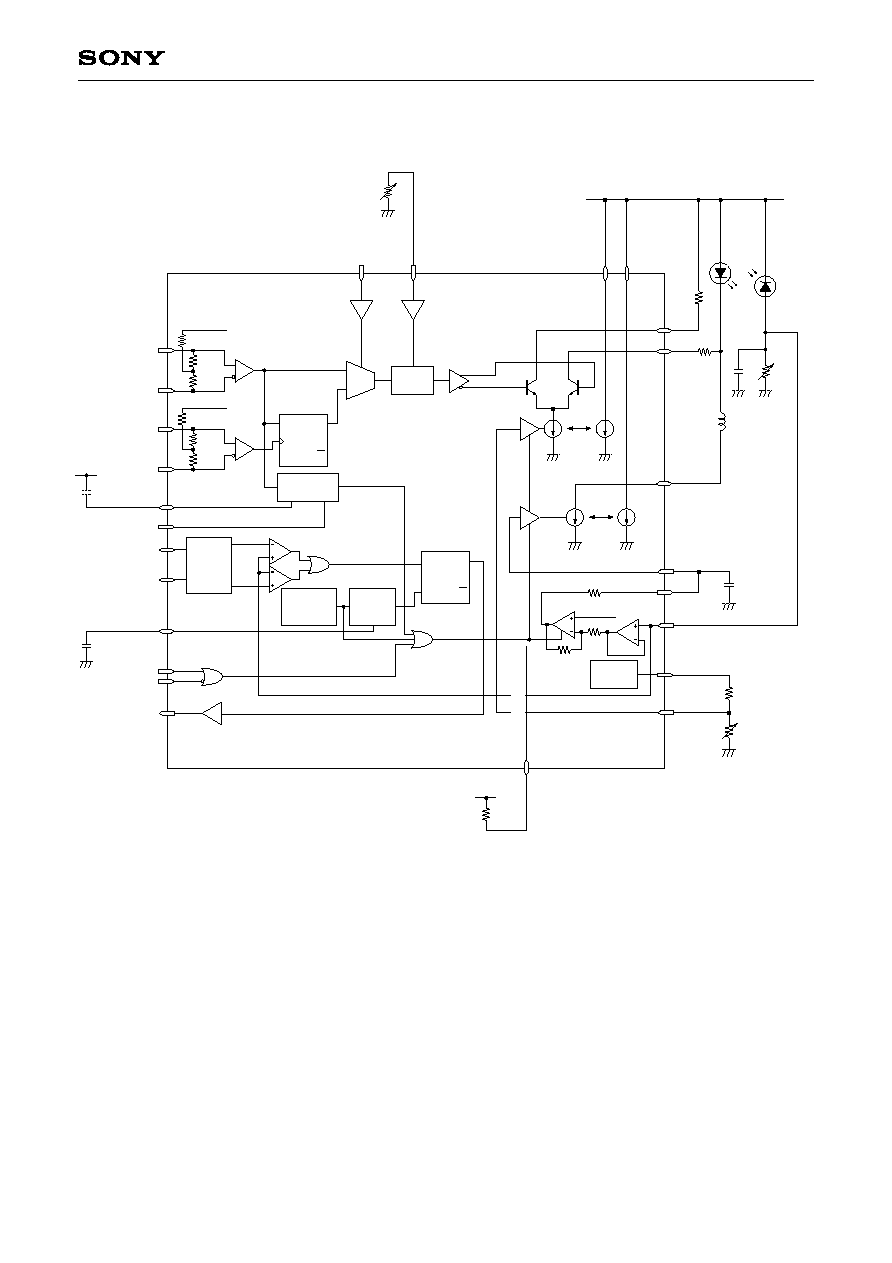
DC Electrical Characteristics Measurement Circuit
50
10k
Vcc 1.4V
50
50
10k
Vcc 1.4V
50
50:1
Duty
Control
Activity Error
Detector
Vcc
Voltage Error
Det.
Time
Stretcher
Vref Gen.
High
Low
MUX
1
D
Q
Q
1.8V
0.3V
0
kill
50:1
4k
Vref 1.1V
15k
60k
kill
S
R
Q
Q
18k
0.4mA
or 2.0mA
Vref
Gen 1.9V
to Modulation/Bias Control
23
21
20
19
24
25
26
27
28
29
30
31
32
1
2
3
4
5
6
22
18
17
15
16
14
13
12
11
10
9
7
8
A
A
A
A
A
A
V
A
A
A
A
A
A
V
V
25
A
A
A
A
A
V
0 to
500µA
V
3.3V
15
CXB1828ER
AC Electrical Characteristics Measurement Circuit
50
10k
Vcc 1.4V
50
50
10k
Vcc 1.4V
50
51
0.1µF
50:1
Duty
Control
Activity Error
Detector
Vcc
Voltage Error
Det.
Time
Stretcher
Vref Gen.
High
Low
MUX
1
D
Q
Q
1.8V
0.3V
0
kill
50:1
4k
Vref 1.1V
15k
60k
kill
S
R
Q
Q
18k
Vref
Gen 1.9V
to Modulation/Bias Control
23
21
20
19
24
25
26
27
28
29
30
31
32
1
2
3
4
5
6
22
18
17
15
16
14
13
12
11
10
9
7
8
25
Z
0
= 50
Oscillo-
scope
50
input
3.3V
Oscilloscope
10k
0 to 100k
10k
0 to 100k
51
0 to 4k
51
0.1µF
51
0.1µF
51
0.1µF
16
CXB1828ER
Application Circuit
Application circuits shown are typical examples illustrating the operation of the devices. Sony cannot assume responsibility for
any problems arising out of the use of these circuits or for any infringement of third party patent and other right due to same.
50
10k
Vcc 1.4V
50
50
10k
Vcc 1.4V
50
50:1
QB
BIAS
BIAS_SET
OP_OUT
OP_IN
VREF
R
VREF
10k
R
MOD_SET
MOD_SET
RREF
R
RREF
Vcc
18k
Q
Duty
Control
R
DUTY
0 to 4k
Activity Error
Detector
Vcc
Voltage Error
Det.
Time
Stretcher
Vref Gen.
High
Low
MUX
1
D
Q
Q
1.8V
0.3V
C
TIME
0.01µF
0
kill
50:1
4k
15k
Vref 1.1V
60k
kill
S
R
Q
Q
Vref
Gen 1.9V
to Modulation/Bias Control
THR
UMODE
DUTY
MOD_MON
BIAS_MON
DIN
DINB
AED_CAP
AED_DISABLE
WCVH
WCVL
TIME_CAP
ALARM
SHUTDOWNB
SHUTDOWN
CKIN
CKINB
C
AED
Vcc
C
APC
0.1µF
R
QB
R
PD
Ferrite
Bead
Laser
Diode
Monitor
Photodiode
R
Q
C
PD
1000pF
17
CXB1828ER
60
50
40
30
20
10
0
0
0.02
0.04
C
TIME
[µF]
Fig. 8. Power-on reset time (T
TIME
) vs. C
TIME
T
TIME
[ms]
0.06
0.08
0.10
160
140
120
100
80
60
40
20
0
0
1
R
DUTY
[k
]
Fig. 9. Increment of output pulse width vs. R
DUTY
Amount of increases in pulse width time [ps]
2
3
4
90
80
70
60
50
40
30
20
10
0
0
500
1000
MOD_SET input voltage [mV]
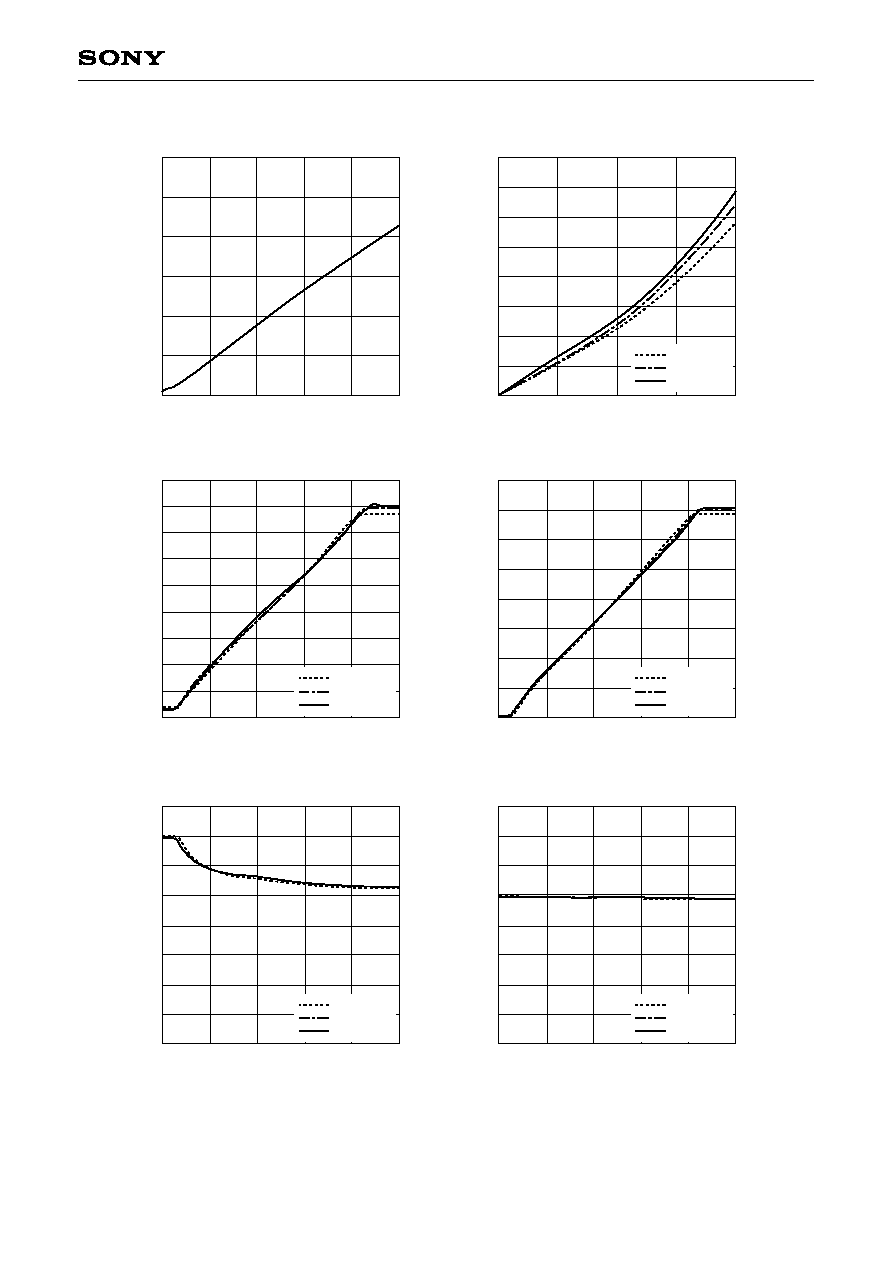
Fig. 10. Modulation current vs.
MOD_SET input voltage
Modulation current [mA]
1500
2000
2500
Fig. 11. Bias current vs. BIAS_SET input voltage
Fig. 12. Ratio of modulation current (I
Q
)
and modulation monitor current vs.
MOD_SET input voltage
Fig. 13. Ratio of bias current (I
B
)
and bias monitor current vs.
BIAS_SET input voltage
Ta = 40°C
Ta = +40°C
Ta = +85°C
Ta = 40°C
Ta = +40°C
Ta = +85°C
80
70
60
50
40
30
20
10
0
0
500
1000
BIAS_SET input voltage [mV]
Bias current [mA]
1500
2000
2500
Ta = 40°C
Ta = +40°C
Ta = +85°C
80
70
60
50
40
30
20
10
0
0
500
1000
BIAS_SET input voltage [mV]
1500
2000
2500
Ta = 40°C
Ta = +40°C
Ta = +85°C
80
70
60
50
40
30
20
10
0
0
500
1000
MOD_SET input voltage [mV]
Ratio of modulation current and
modulation monitor current [mA]
Ratio of bias current and bias monitor current [mA]
1500
2000
2500
Ta = 40°C
Ta = +40°C
Ta = +85°C
Example of Representative Characteristics
18
CXB1828ER
100
90
70
80
60
50
40
20
30
10
0
0
200
C
AED
[pF]
Time base: 100.0ps/div
250mV/div
RL = 25
Ta = 25°C
I
Q
= 30mA
Pattern = PRBS
23
1
Data Rate = 2.5Gbps
Fig. 14. Activity error detect time (T
AED
) vs.
C
AED
Fig. 16. Electrical Output Waveform
T
AED
(AED error detection time) [µs]
400
800
600
100
Ta = 40°C
Ta = +40°C
Ta = +85°C
3.0
2.8
2.6
2.4
2.2
2.0
1.8
1.6
1.4
1.2
1.0
0.8
0.6
0.4
0.2
0
0
0.4
OP_IN input voltage [V]
Fig. 15. OP_OUT output voltage vs.
OP_IN input voltage
OP_OUT output v
oltage [V]
0.8
1.6
1.2
0.2
0.6
1.4
1.8
1.0
2.0
Ta = 40°C
Ta = +40°C
Ta = +85°C
Time base: 100.0ps/div
FP LD (
= 1310nm)
Ta = 25°C
Pattern = PRBS
23
1
Data Rate = 2.5Gbps
Filter
Mask: OC-48
Fig. 17. Optical Output Waveform
2
3
1
Vcc = 3.3V
19
CXB1828ER
2.3
4.8
IC pin size
Via hole in PWB
Package outline
V
EE
in PWB
V
EE
or solder resist in PWB
(This area is V
EE
in IC)
0.8
0.2
0.14
0.4
0.6 ± 0.2
0.15
0.39
Foot pattern
recommended
Foot Print Unit: mm

20
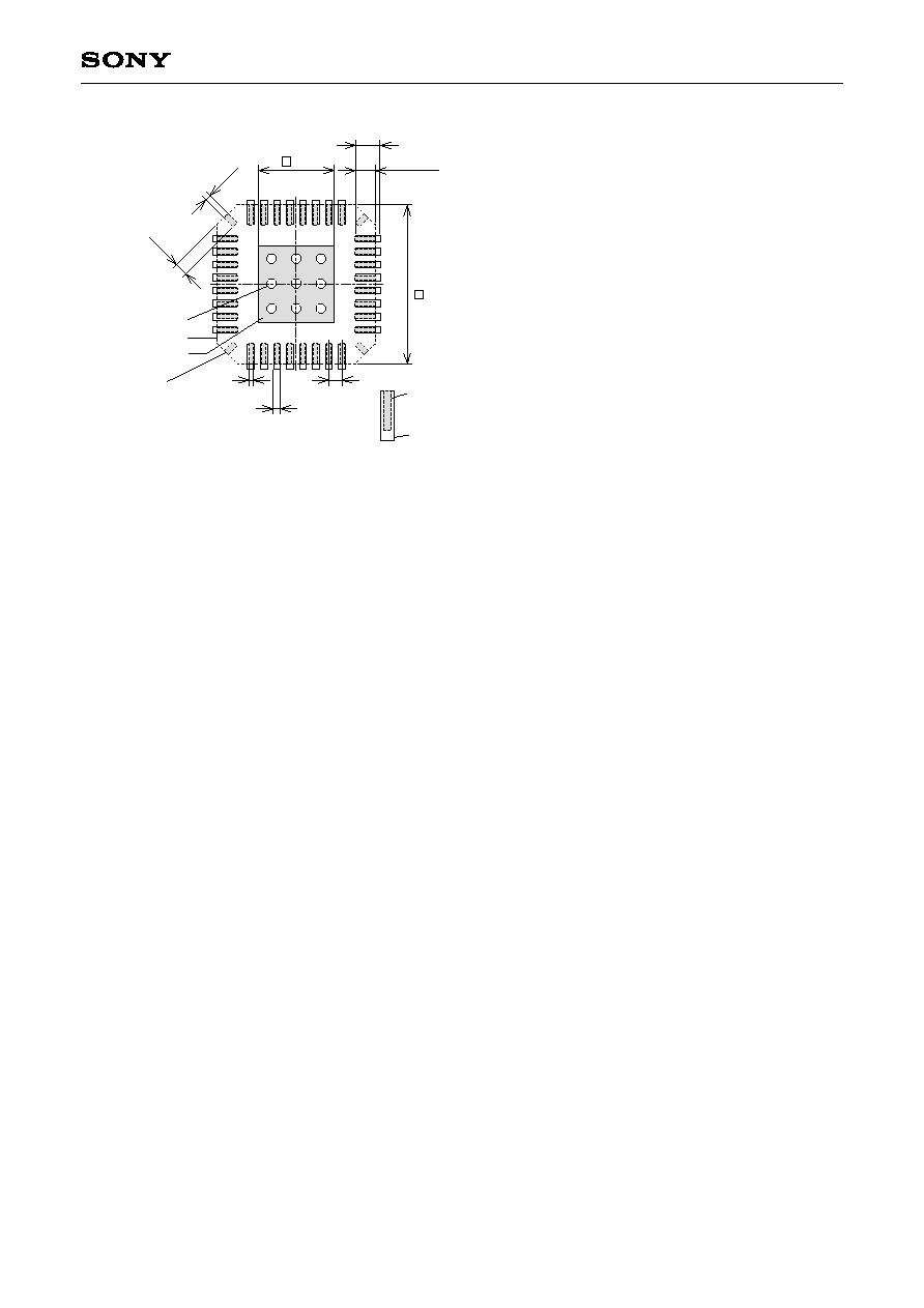
CXB1828ER
Package Outline Unit: mm
SONY CODE
EIAJ CODE
JEDEC CODE
PACKAGE MATERIAL
LEAD TREATMENT
LEAD MATERIAL
PACKAGE MASS
EPOXY RESIN
SOLDER PLATING
COPPER ALLOY
PACKAGE STRUCTURE
VQFN-32P-04
32PIN VQFN (PLASTIC)
0.05g
2.3
4-R0.3
S
S A-B C
S A-B C
C 0.6
(0.15)
0.9 ±
0.7
0.05 S
0.6 ± 0.1
x4
0.1
x4
0.1
0.05 M S A-B C
0.4
A
1
8
9
16
17
24
25
32
B
4.8
4.4
C
1.4
PIN1 INDEX
45°
TERMINAL SECTION
0.2 ±
0.01
0.23 ±
Solder Plating
0.14 0.03
0.13 ± 0.025
+ 0.09
(Stand Off)
0.1
(0.39)
ranges of 0.1mm and 0.25mm from the end of a terminal.
NOTE: 1) The dimensions of the terminal section apply to the
2) The dimension of (
1) is apply to DiePad and the lead.
0.03 ±
0.03(
1)
0.02
LEAD PLATING SPECIFICATIONS
ITEM
LEAD MATERIAL
COPPER ALLOY
SOLDER COMPOSITION
Sn-Bi Bi:1-4wt%
PLATING THICKNESS
5-18µm
SPEC.
SONY CODE
EIAJ CODE
JEDEC CODE
PACKAGE MATERIAL
LEAD TREATMENT
LEAD MATERIAL
PACKAGE MASS
EPOXY RESIN
SOLDER PLATING
COPPER ALLOY
PACKAGE STRUCTURE
VQFN-32P-04
32PIN VQFN (PLASTIC)
0.05g
2.3
4-R
0.3
S
S A-B C
S A-B C
C
0.6
(0.15)
0.9 ±
0.7
0.05 S
0.6 ± 0.1
x4
0.1
x4
0.1
0.05 M S A-B C
0.4
A
1
8
9
16
17
24
25
32
B
4.8
4.4
C
1.4
PIN1 INDEX
45°
TERMINAL SECTION
0.2 ±
0.01
0.23 ±
Solder Plating
0.14 0.03
0.13 ± 0.025
+ 0.09
(Stand Off)
0.1
(0.39)
ranges of 0.1mm and 0.25mm from the end of a terminal.
NOTE: 1) The dimensions of the terminal section apply to the
2) The dimension of (
1) is apply to DiePad and the lead.
0.03 ±
0.03(
1)
0.02
Sony Corporation