
CXB1810FN
Post Amplifier for Optical Fiber Communication Receiver
Description
The CXB1810FN achieves 2R optical fiber
communication receiver functions (Reshaping and
Regenerating) on a single chip.
This IC is equipped with a signal detection function,
and outputs at TTL level.
Features
ñ Auto-offset canceler circuit
ñ Signal interruption alarm output
ñ Single 3.3V or 5.0V power supply
Applications
SONET/SDH
Absolute Maximum Ratings
ñ Supply voltage
V
CC
Ù V
EE
Ù0.3 to +6.0
V
ñ Input voltage difference
|
V
D
Ù V
DN
|
2.5
V
ñ ECL/TTL output current (Continuous)
50
mA
(Surge)
70
mA
ñ Storage temperature
Tj
Ù65 to +150
¯C
Recommended Operating Conditions
ñ Supply voltage
V
CC
Ù V
EE
3.14 to 5.25
V
ñ Termination voltage (for Q/QB)
Vt1
V
CC
Ù 1.8 to Vcc Ù 2.2
V
ñ Termination resistance (for Q/QB)
Rt
46 to 56
ñ Operating temperature
Ta
Ù40 to +85
¯C
Ù 1 Ù
E99801D26-PS
Sony reserves the right to change products and specifications without prior notice. This information does not convey any license by
any implication or otherwise under any patents or other right. Application circuits shown, if any, are typical examples illustrating the
operation of the devices. Sony cannot assume responsibility for any problems arising out of the use of these circuits.
16 pin HSOF (plastic)
Ù 2 Ù
CXB1810FN
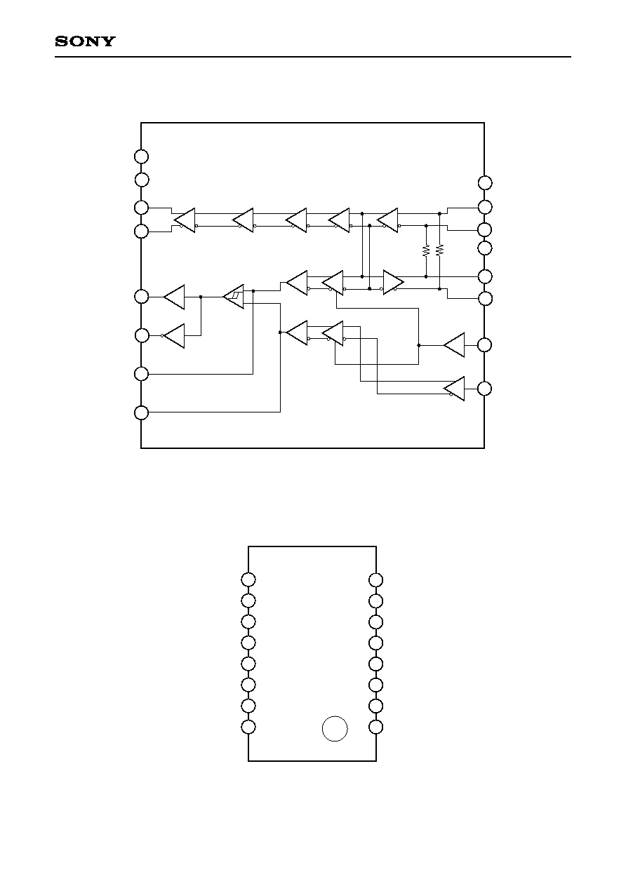
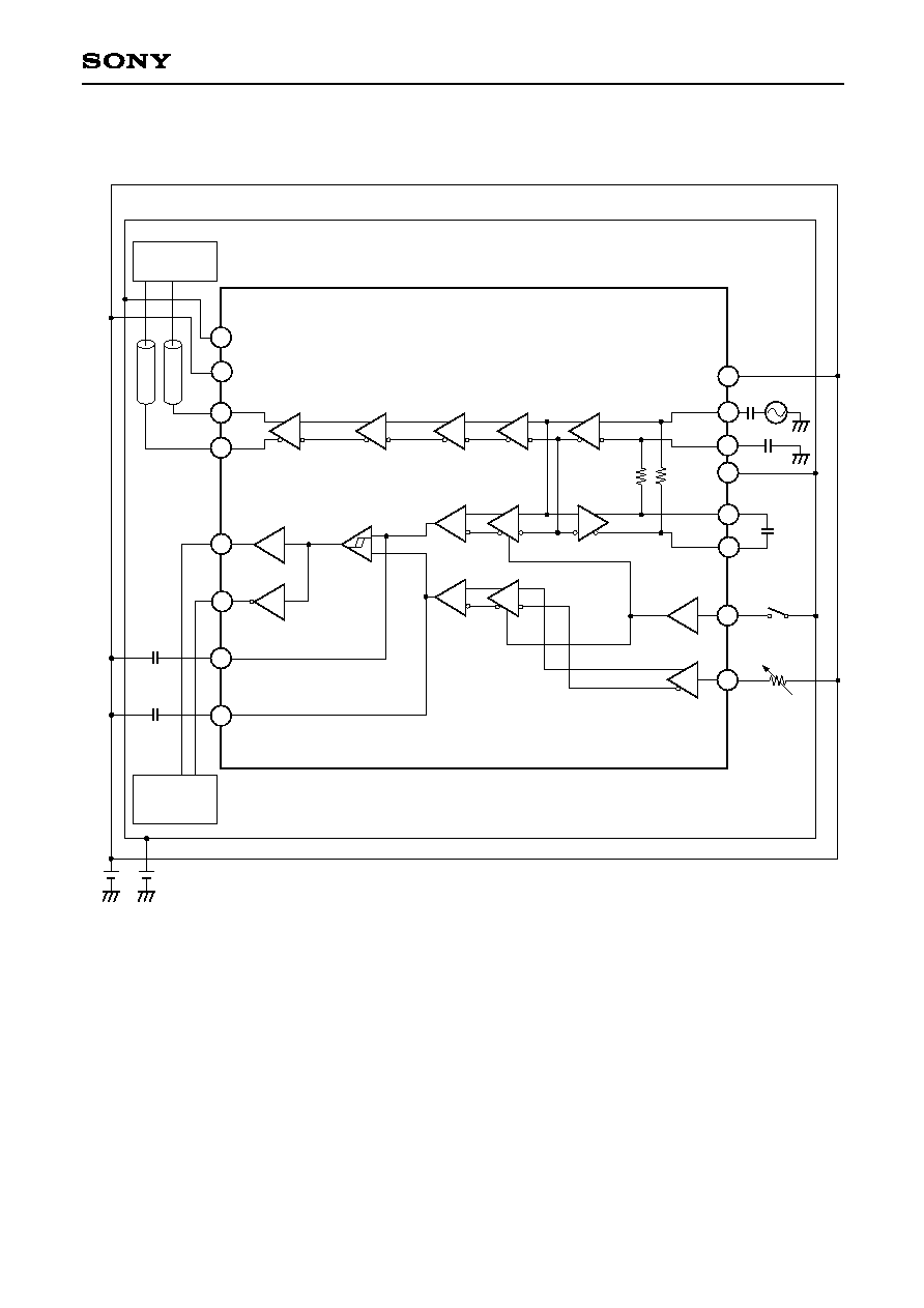
Block Diagram
Q
D
Vcc
V
EE
DB
CAP1
CAP1B
SW
DOWN
QB
V
EE
O
VccO
CAP3
CAP2
SDC
SDCB
1
2
3
4
5
6
7
8
9
10
11
12
13
14
15
16
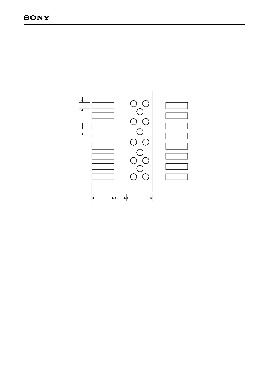
Pin Configuration
1
2
3
4
5
6
7
8
9
10
11
12
13
14
15
16
CAP2
CAP3
SDCB
SDC
QB
Q
V
CC
O
V
EE
O
DOWN
SW
CAP1B
CAP1
V
EE
DB
D
V
CC
Ù 3 Ù
CXB1810FN
Pin
No.
Symbol
Typical pin
voltage (V)
DC
AC
Equivalent circuit
Description
3
4
V
CC
O
V
EE
O
1
V
EE
O
0
Ground for data output circuit.
2
VccO
3.3 or
5.0
Positive power supply for data
output circuit.
5
V
CC
V
EE
3
4
Q
QB
1.7
to
2.4
or
3.4
to
4.1
Data outputs.
5
SDC
0.2
to
2.9
or
0.2
to
4.7
Signal detection output (TTL).
The SDC output is driven to low
level while signal interruption is
detected.
Pin Description
6
V
CC
V
EE
8
7
V
CC
V
EE
6
SDCB
0.2
to
2.9
or
0.2
to
4.7
Signal detection output (TTL).
The SDCB output is driven to
high level while signal
interruption is detected.
7
8
CAP3
CAP2
1.6 or
3.3
1.3
to
1.8
or
3.0
to
3.5
Connect a peak hold capacitor
for the signal detection circuit.
470pF (typ.)

Ù 4 Ù
CXB1810FN
9
V
CC
V
EE
10
V
CC
V
EE
Pin
No.
Symbol
Typical pin
voltage (V)
DC
AC
Equivalent circuit
Description
9
DOWN
2.4 or
4.1
Connect a resistor between this
pin and the V
CC
pin to decrease
the signal detection level from
the default value.
10
SW
Switches the maximum
identification voltage amplitude.
This pin is set to 50mVp-p
(single ended) when open or high
level, or to 15mVp-p (single
ended) when low level.
Setting to low level is
recommended when using a
resistor of 510
or less between
the V
CC
and DOWN pins.
11
12
CAP1B
CAP1
14
15
DB
D
2.2 or
3.9
Connect an external capacitor
between these pins.
0.022çF (typ.)
Data inputs.
13
V
EE
0
Ground.
16
V
CC
3.3 or
5.0
Positive power supply.
11
12
14
15
V
CC
V
EE
Ù 5 Ù
CXB1810FN
Electrical Characteristics
DC Characteristics
(V
CC
= 3.14 to 5.25V, Ta = Ù40 to +85¯C, unless otherwise specified)
Item
Q/QB high output voltage
Q/QB low output voltage
Q/QB output amplitude
SDC/SDCB high output voltage
SDC/SDCB low output voltage
SW high input voltage
SW low input voltage
Maximum input voltage
amplitude
D/DB input resistance
Supply current
VOH1
VOL1
Vp
VOHT
VOLT
VIHT
VILT
Vmax
Rin
ICC
51
terminated to V
CC
Ù 2V
51
terminated to V
CC
Ù 2V
51
terminated to V
CC
Ù 2V
IOH = Ù0.2mA
IOL = 2.1mA
During single-phase input
All outputs open
V
CC
Ù 1100
V
CC
Ù 1800
500
2.4
V
CC
Ù 0.3
V
EE
1000
33
50
40
V
CC
Ù 650
V
CC
Ù 1300
1000
0.5
V
CC
V
EE
+ 0.3
69
55
mV
mV
mVp-p
V
V
V
V
mVp-p
mA
Symbol
Min.
Typ.
Max.
Unit
Conditions
Item
Limiting amplifier gain
Signal detection threshold voltage
Signal detection hysteresis width
Signal detection response assert time
1
Signal detection response deassert time
1
Q/QB rise time (20 to 80%)
Q/QB fall time (20 to 80%)
GL
Vth
P
Tas
Tdas
TR
TF
During single ended input
51
terminated to V
CC
Ù 2V
51
terminated to V
CC
Ù 2V
45
3
0
2.3
34
6
130
110
8
100
100
dB
mVp-p
dB
çs
çs
ps
ps
Symbol
Min.
Typ.
Max.
Unit
Conditions
AC Characteristics
(V
CC
= 3.14 to 5.25V, Ta = Ù40 to +85¯C, unless otherwise specified)
1
Data = PN23 Ù 1 pattern, 100mVp-p single ended, Rd = open, CAP2/CAP3 = 470pF
Ù 6 Ù
CXB1810FN
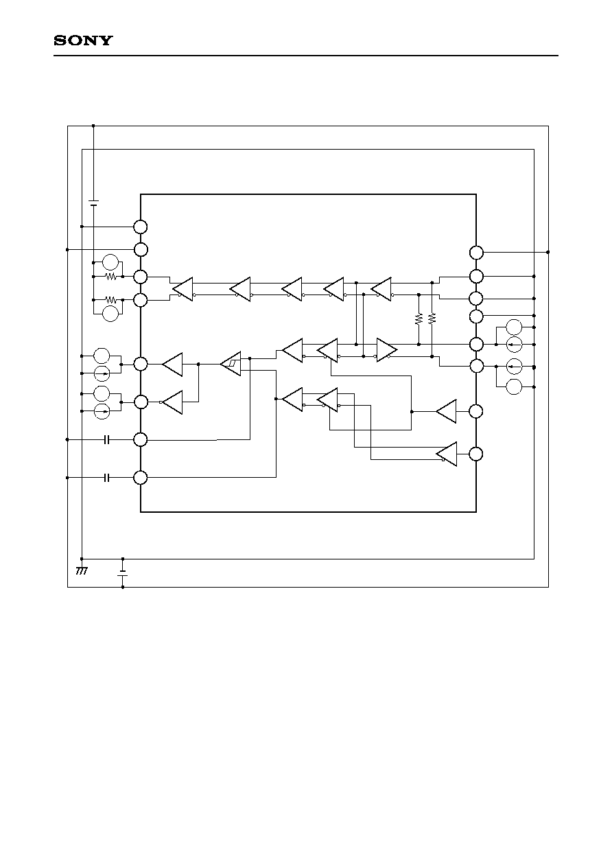
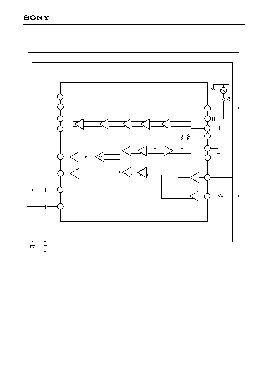
DC Electrical Characteristics Measurement Circuit
V
V
51
2V
51
3.14 to 5.25V
V
V
470pF
470pF
V
V
1
2
3
4
5
6
7
8
9
10
11
12
13
14
15
16
Ù 7 Ù
CXB1810FN
AC Electrical Characteristics Measurement Circuit
0.022
ç
F
0.01
ç
F
0.01
ç
F
Ù1.14 to Ù3.25V
2V
470pF
470pF
ZO = 50
ZO = 50
50
input
Oscilloscope
Hi-Z input
Oscilloscope
1
2
3
4
5
6
7
8
9
10
11
12
13
14
15
16
Ù 8 Ù
CXB1810FN
Application Circuit
0.022
ç
F
0.01
ç
F
0.01
ç
F
51
3.3/5.0V
470pF
470pF
1
2
3
4
5
6
7
8
9
10
11
12
13
14
15
16
Application circuits shown are typical examples illustrating the operation of the devices. Sony cannot assume responsibility for
any problems arising out of the use of these circuits or for any infringement of third party patent and other right due to same.
Ù 9 Ù
CXB1810FN
R1
R2
C1
C1
R1
C2
15
14
12
11
R2
To inside the IC
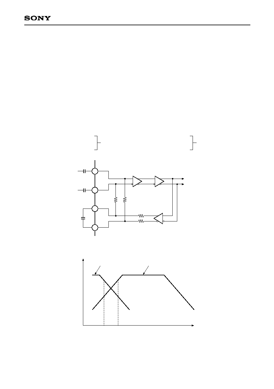
Fig. 1
DC feedback frequency
response
Frequency
f1
f2
Gain
Amplifier frequency
response
Fig. 2
Notes on Operation
1. Limiting amplifier block
The limiting amplifier block is equipped with an auto-offset canceler circuit. When external capacitors C1 and
C2 are connected as shown in Fig. 1, the DC bias is set automatically in this block.
External capacitor C1 and internal resistor R1 determine the input low cut-off frequency f2 as shown in Fig. 2.
Similarly, external capacitor C2 and internal resistor R2 determine the high cut-off frequency for DC feedback.
Since a peak may occur in the low frequency area of the gain characteristics depending on the f1/f2
combination, set the C1 and C2 values so as to avoid the occurrence of this peak. The typical values of R1,
R2, C1 and C2 are indicated below.
Also, when a single ended input is used, provide AC grounding by connecting Pin 14 to a capacitor which has
the same capacitance as capacitor C1.
R1 (internal): 50
R2 (internal): 10k
f2: 318kHz
f1: 723Hz
C1 (external): 0.01çF
C2 (external): 0.022çF
Ù 10 Ù
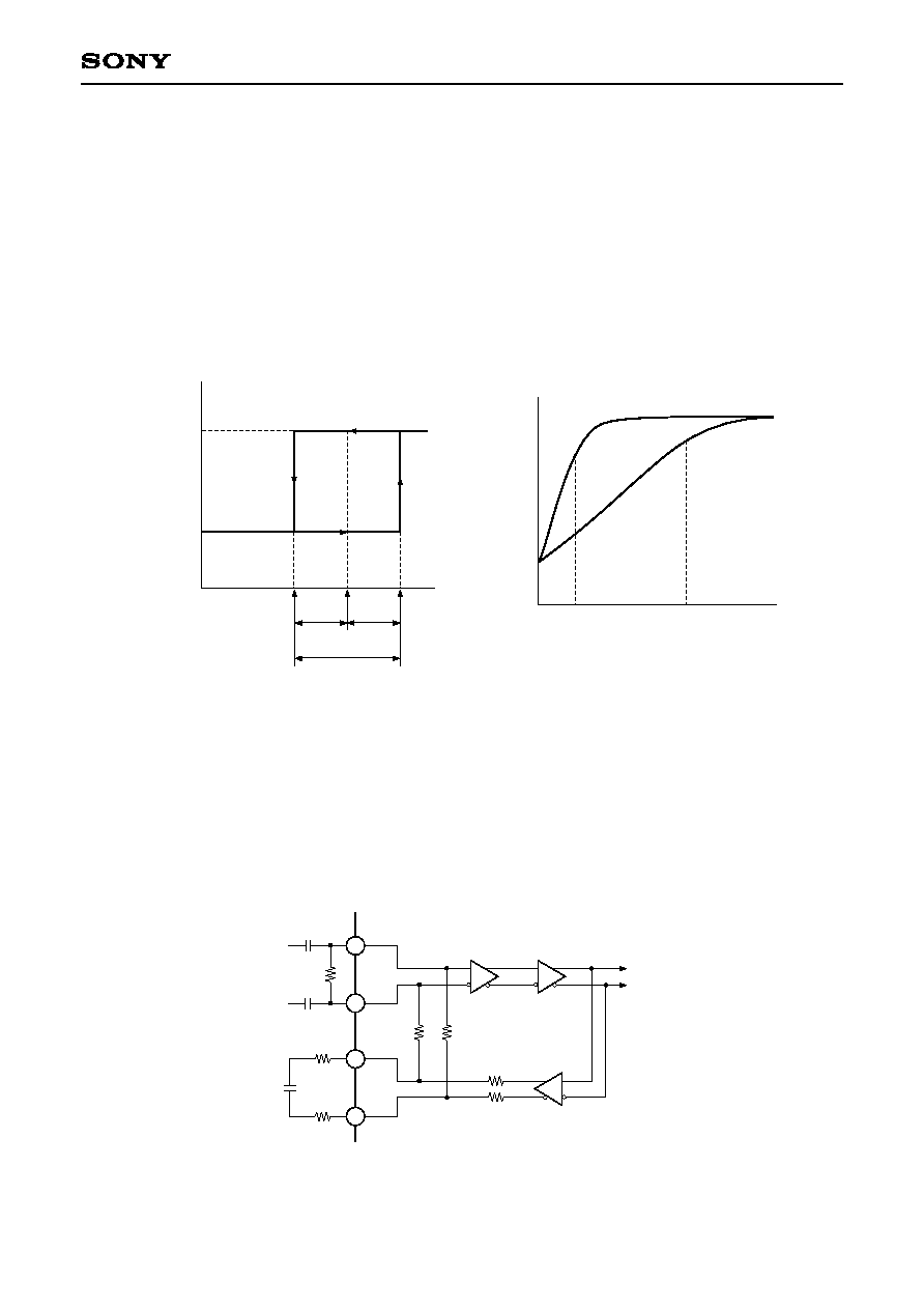
CXB1810FN
Low level
VDAS
Deassert level
VAS
Assert level
VAS
VDAS
3dB
3dB
Hysteresis
High level
SD output
C1
C1
C2
15
14
12
11
100
1.5k
1.5k
R1
R2
R1
R2
To inside the IC
Fig. 5
2. Alarm block
In this block, the input signal amplitude is detected and the signal interruption alarm is output when the
amplitude becomes lower than the set alarm level. The alarm level setting can be adjusted by connecting an
external resistor Rd between the DOWN and V
CC
pins.
Also, this IC can set the maximum identification voltage amplitude to two levels. The maximum identification
voltage amplitude is set to 50mVp-p (single ended) when the SW pin is open or high level, or to 15mVp-p
(single ended) when the SW pin is low level.
Figs. 15 and 16 show the relation of Rd and the alarm assert/deassert level. Setting the SW pin to low level is
recommended when Rd is 510
or less.
Fig. 3
SW
Low
15
50
SW
High
Input voltage (mVp-p, single phase)
Fig. 4
In addition, the SD response deassert time is guaranteed only under the conditions noted in the AC Electrical
Characteristics item, but the response becomes delayed as the input signal amplitude becomes larger. This is
because the input resistor R1 shown in Fig. 1 is small at 50
, so the charge accumulated in C2 is relatively
large and the discharge time for this charge accounts for most of the SD response deassert time. The SD
response deassert time can be shortened by using the external circuit shown in Fig. 5 or by shorting the CAP1
and CAP1B pins. However, care should be taken as the auto-offset canceler circuit does not operate in this
case causing the reception sensitivity to deteriorate. Fig. 14 shows the relation between the SD response
deassert time and the electrical input amplitude when using the connection shown in Fig. 5.
Ù 11 Ù
CXB1810FN
4. Other
ñ Be careful when handling this IC as its electrostatic discharge strength is weak.
ñ Be sure to connect all power supply pins (V
CC
O, V
CC
) and ground pins (V
EE
O, V
EE
) to power supplies or
grounds, respectively. For example, if only V
CC
O is left open and power is supplied to the other pin, the IC
may malfunction.
3. Substrate layout
The exposed metal portions on the rear surface of the package used for the CXB1810FN are electrically
connected to the silicon substrate. Superior thermal radiation characteristics can be obtained by connecting
the rear surface of the package and these exposed metal portions to the ground surface on the PCB.
Providing lands directly below the package as shown in the figure below and connecting as many thermal vias
as possible to the inner layer ground surface is recommended.
0.75mm
1.45mm
0.4mm
0.25mm
2.0mm
Ù 12 Ù
CXB1810FN
Example of Representative Characteristics
4.5
5.0
3.0
3.5
4.0
5.5
Q/QB output voltage amplitude
vs. Supply voltage
V
CC
[V]
Q/QB output voltage amplitude [Vp-p]
0.650
0.660
0.680
0.685
0.690
0.695
0.700
0.655
0.665
0.670
0.675
Vp-p, Ta = 40
¯
C
Q/QB output voltage amplitude
vs. Temperature
Ta [
¯
C]
Q/QB output voltage amplitude [Vp-p]
40
60
80
Ù40
0.650
0.660
0.655
0.665
0.675
0.670
0.685
0.680
0.690
0.700
0.695
20
0
Ù20
100
V
CC
= 3.14V/5.25V
V
CC
= 3.14V
V
CC
= 5.25V
Q/QB output voltage vs. Supply voltage
V
CC
[V]
Q/QB output voltage [V, ref to V
CC
]
4.5
5.0
3.0
Ù1.6
Ù1.3
Ù1.2
Ù1.5
Ù1.4
Ù0.9
Ù0.8
Ù1.1
Ù1.0
3.5
4.0
5.5
Ta = 40
¯
C
ICC vs. Supply voltage
V
CC
[V]
I
CC
[mA]
4.0
4.5
5.0
3.0
38.5
39.0
39.5
40.0
41.0
40.5
41.5
3.5
5.5
Ta = 40
¯
C
Output pins open
ICC vs. Temperature
Ta [
¯
C]
I
CC
[mA]
80
Ù20
Ù40
20
0
60
40
37.0
40.0
40.5
41.0
41.5
42.0
37.5
38.0
38.5
39.0
39.5
100
V
CC
= 3.14V/5.25V
Output pins open
V
CC
= 3.14V
V
CC
= 5.25V
Q/QB output voltage vs. Temperature
Ta [
¯
C]
Q/QB output voltage [V, ref to V
CC
]
80
Ù20
Ù40
20
0
60
40
Ù1.8
Ù1.4
Ù1.6
Ù1.2
Ù0.6
Ù0.8
Ù1.0
100
V
CC
= 3.14V/5.25V
H level (V
CC
= 3.14V)
H level (V
CC
= 5.25V)
L level (V
CC
= 3.14V)
L level (V
CC
= 5.25V)
Fig. 6
Fig. 7
Fig. 8
Fig. 9
Fig. 10
Fig. 11
Ù 13 Ù
CXB1810FN
H level (V
CC
= 3.14V)
H level (V
CC
= 5.25V)
L level (V
CC
= 3.14V)
L level (V
CC
= 5.25V)
0
1
3
5
6
2
4
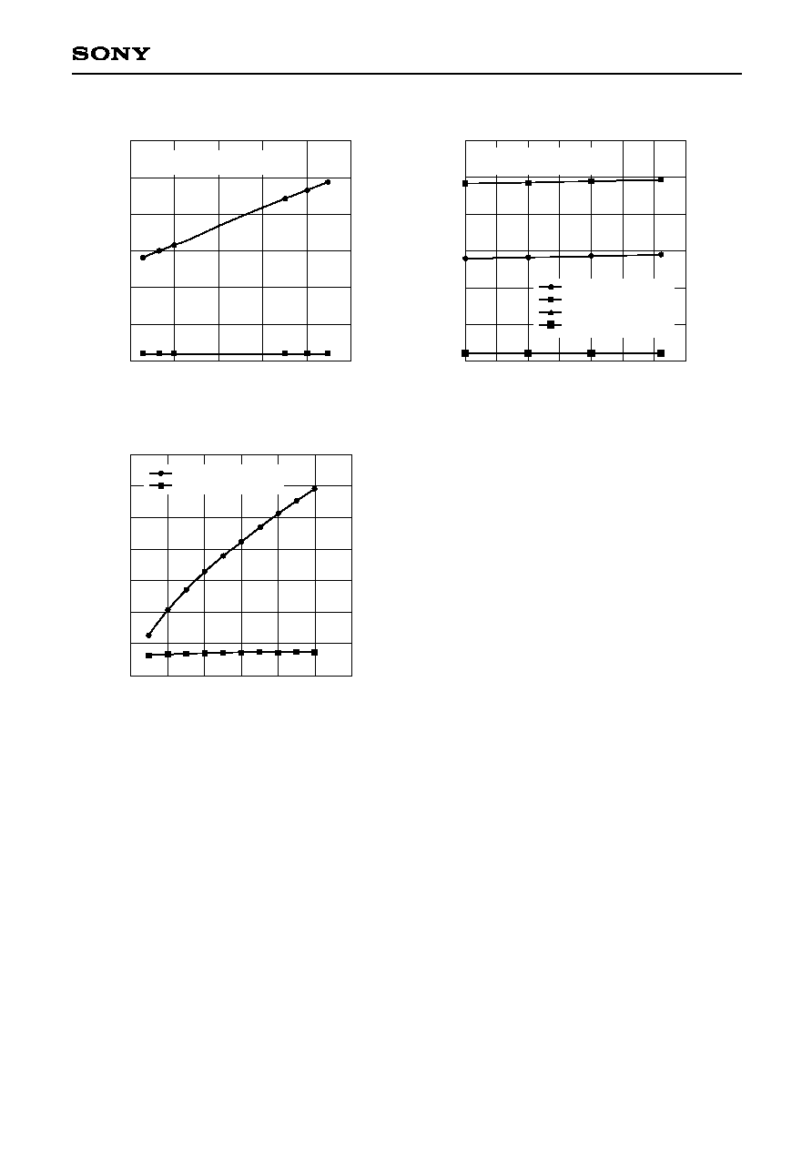
SDC/SDCB output voltage vs. Temperature
Ta [
¯
C]
SDC/SDCB output voltage [V]
40
60
80
Ù40
20
0
Ù20
100
V
CC
= 3.14V/5.25V,
IOH = Ù0.2mA, IOL = +2.1mA
SDC/SDCB output voltage vs. Supply voltage
V
CC
[V]
SDC/SDCB output voltage [V]
4.5
4.0
5.0
3.0
3.5
0
1
3
5
6
2
4
5.5
Ta = 40
¯
C,
IOH = Ù0.2mA, IOL = +2.1mA
Fig. 12
Fig. 13
Input voltage amplitude
vs. SD response deassert time
Input voltage amplitude [mVp-p, single ended]
SD response deassert time [
ç
s]
1.0
0
0.4
0.2
0.8
0.6
0
350
50
150
100
200
250
300
1.2
Recommended circuit
Fig. 5 connection
Fig. 14

Ù 14 Ù
CXB1810FN
Rd vs. SD assert/deassert level
Rd [k
]
SD assert/deassert level [mVp-p, single ended]
1
10
0.1
0
10
20
30
50
40
60
100
V
CC
= 3.3V
SW = H level
VAS
VDAS
Rd vs. SD assert/deassert level
Rd [
]
SD assert/deassert level [mVp-p, single ended]
600
100
300
200
500
400
0
14
16
2
6
4
8
10
12
700
V
CC
= 3.3V
SW = L level
VAS
VDAS
SD assert/deassert level vs. Supply voltage
V
CC
[V]
SD assert/deassert level [mVp-p, single ended]
4.5
5.0
3.0
0
30
40
10
20
60
50
3.5
4.0
5.5
Ta = 40
¯
C,
DOWN pin open,
SW = H level
VAS
VDAS
0
15
20
5
10
30
25
4.5
5.0
3.0
3.5
4.0
5.5
SD assert/deassert level vs. Supply voltage
V
CC
[V]
SD assert/deassert level [mVp-p, single ended]
Ta = 40
¯
C,
Rd = 2k
,
SW = H level
VAS
VDAS
0
15
20
5
10
30
25
SD assert/deassert level vs. Temperature
Ta [
¯
C]
SD assert/deassert level [mVp-p, single ended]
40
60
80
Ù40
20
0
Ù20
100
V
CC
= 3.14V/5.25V,
Rd = 2k
,
SW = H level
VAS (V
CC
= 3.14V)
VDAS (V
CC
= 3.14V)
VAS (V
CC
= 5.25V)
VDAS (V
CC
= 5.25V)
SD assert/deassert level vs. Temperature
Ta [
¯
C]
SD assert/deassert level [mVp-p, single ended]
80
Ù20
Ù40
20
0
60
40
0
20
10
30
60
50
40
100
V
CC
= 3.14V/5.25V,
DOWN pin open,
SW = H level
VAS (V
CC
= 3.14V)
VDAS (V
CC
= 3.14V)
VAS (V
CC
= 5.25V)
VDAS (V
CC
= 5.25V)
Fig. 15
Fig. 16
Fig. 17
Fig. 18
Fig. 19
Fig. 20

Ù 15 Ù
CXB1810FN
SD assert/deassert level vs. Supply voltage
Ta [
¯
C]
SD assert/deassert level [mVp-p, single ended]
4.5
5.0
3.0
0
6
8
2
4
14
12
10
3.5
4.0
5.5
Ta = 40
¯
C,
Rd = 510
,
SW = L level
VAS
VDAS
0
4
5
1
3
7
2
6
4.5
5.0
3.0
3.5
4.0
5.5
SD assert/deassert level vs. Supply voltage
V
CC
[V]
SD assert/deassert level [mVp-p, single ended]
Ta = 40
¯
C,
Rd = 150
,
SW = L level
VAS
VDAS
0
4
5
1
3
7
2
6
SD assert/deassert level vs. Temperature
Ta [
¯
C]
SD assert/deassert level [mVp-p, single ended]
40
60
80
Ù40
20
0
Ù20
100
V
CC
= 3.14V/5.25V,
Rd = 150
,
SW = L level
VAS (V
CC
= 3.14V)
VDAS (V
CC
= 3.14V)
VAS (V
CC
= 5.25V)
VDAS (V
CC
= 5.25V)
SD assert/deassert level vs. Temperature
Ta [
¯
C]
SD assert/deassert level [mVp-p, single ended]
80
Ù20
Ù40
20
0
60
40
0
4
2
6
14
12
8
10
100
V
CC
= 3.14V/5.25V,
Rd = 510
,
SW = L level
VAS (V
CC
= 3.14V)
VDAS (V
CC
= 3.14V)
VAS (V
CC
= 5.25V)
VDAS (V
CC
= 5.25V)
Fig. 21
Fig. 22
Fig. 23
Fig. 24
1.00E-10
1.00E-06
1.00E-05
1.00E-09
1.00E-07
1.00E-03
1.00E-08
1.00E-04
Input amplitude vs. Bit error rate (V
CC
= 5.0V)
Input amplitude [mVp-p, single ended]
Bit error rate
4.0
4.5
5.0
2.0
3.5
3.0
2.5
5.5
6.0
Ta = Ù40
¯
C
Ta = 0
¯
C
Ta = 40
¯
C
Ta = 85
¯
C
Fig. 26
1.00E-10
1.00E-06
1.00E-05
1.00E-09
1.00E-07
1.00E-03
1.00E-08
1.00E-04
Input amplitude vs. Bit error rate (V
CC
= 3.3V)
Input amplitude [mVp-p, single ended]
Bit error rate
4.0
4.5
5.0
2.0
3.5
3.0
2.5
5.5
6.0
Ta = Ù40
¯
C
Ta = 0
¯
C
Ta = 40
¯
C
Ta = 85
¯
C
Fig. 25
Ù 16 Ù
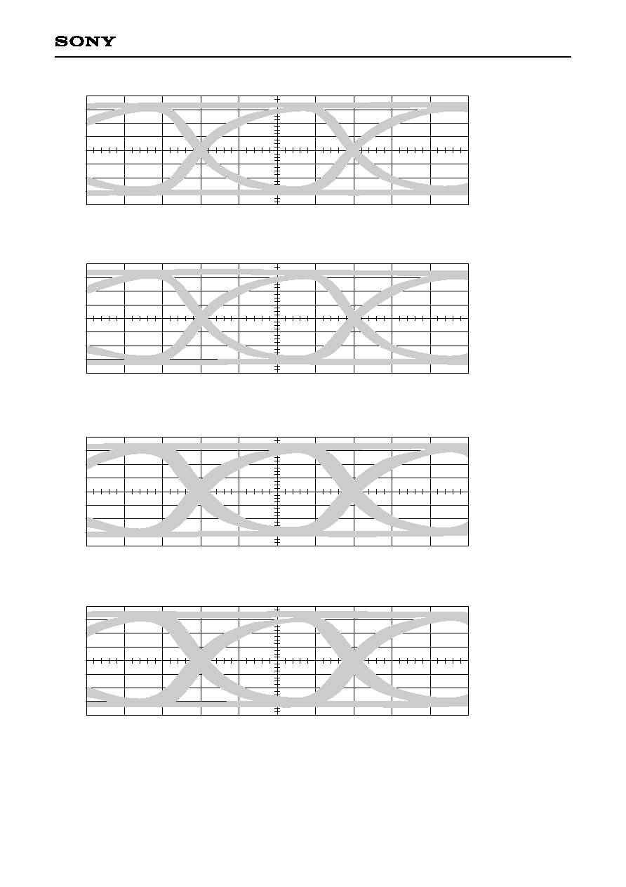
CXB1810FN
100ps/div
100mV/div
Q output waveform
V
CC
= 3.3V, Ta = 40
¯
C
D = 100mVp-p
(single ended)
PN23 pattern
100ps/div
100mV/div
Q output waveform
V
CC
= 5.0V, Ta = 40
¯
C
D = 100mVp-p
(single ended)
PN23 pattern
100ps/div
100mV/div
Q output waveform
V
CC
= 3.3V, Ta = 40
¯
C
D = 10mVp-p
(single ended)
PN23 pattern
100ps/div
100mV/div
Q output waveform
V
CC
= 5.0V, Ta = 40
¯
C
D = 10mVp-p
(single ended)
PN23 pattern
Fig. 27
Fig. 28
Fig. 29
Fig. 30
Ù 17 Ù
CXB1810FN
Sony Corporation
SONY CODE
EIAJ CODE
JEDEC CODE
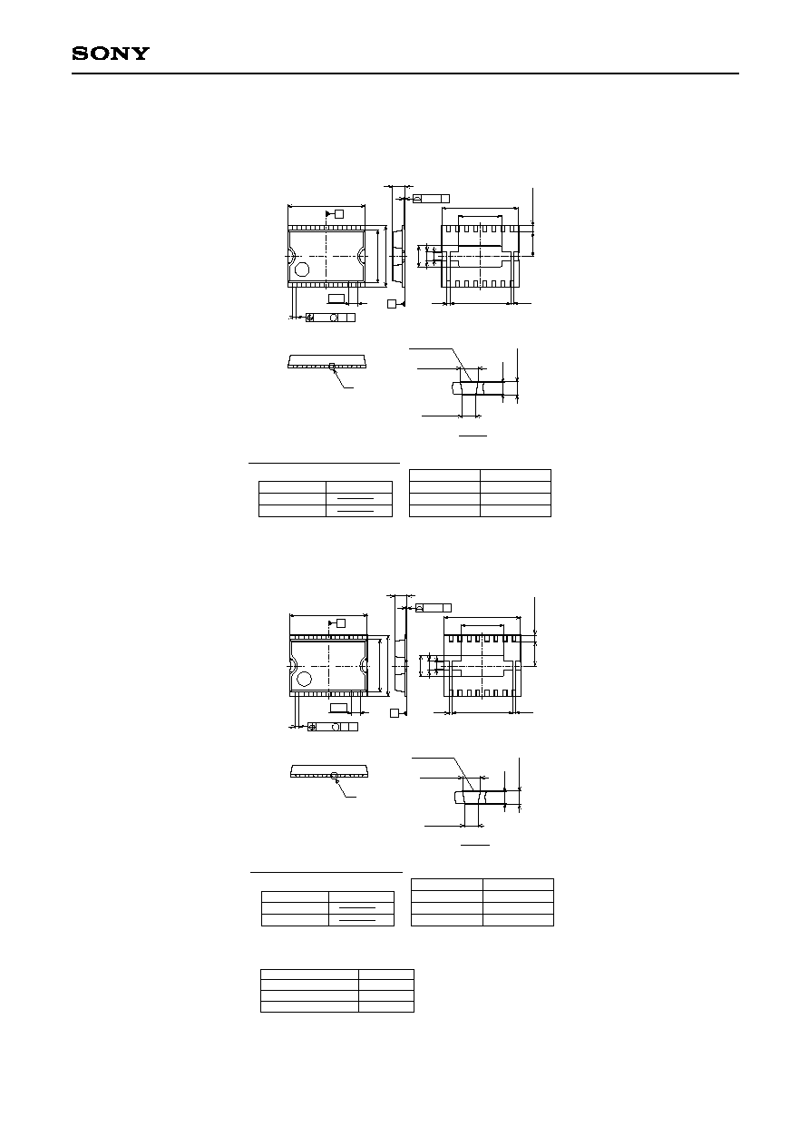
PACKAGE MATERIAL
LEAD TREATMENT
LEAD MATERIAL
PACKAGE MASS
EPOXY RESIN
SOLDER PLATING
COPPER ALLOY
PACKAGE STRUCTURE
0.06g
HSOF 16PIN(PLASTIC)
NOTE: Dimension "
" does not include mold protrusion.
B
0.9 Ý 0.1
(5.5)
(3.1)
(1.75)
(0.2)
(0.2)
(4.4)
(1.5)
(0.7)
(0.5)
S
0.45 Ý
0.15
0.05
5.6 Ý 0.1
0.65
8
1
9
16
3.8 Ý
0.1
4.4 Ý
0.1
A
M S A
S
0.05
0.32 Ù 0.03
+ 0.1
0.26 Ù 0.03
+ 0.1
(0.2)
0.2 0
+ 0.05
Solder Plating
DETAILB
HSOF-16P-02
Package Outline
Unit: mm
LEAD PLATING SPECIFICATIONS
ITEM
LEAD MATERIAL
COPPER ALLOY
SOLDER COMPOSITION
Sn-Bi Bi:1-4wt%
PLATING THICKNESS
5-18
ç
m
SPEC.
SONY CODE
EIAJ CODE
JEDEC CODE
PACKAGE MATERIAL
LEAD TREATMENT
LEAD MATERIAL
PACKAGE MASS
EPOXY RESIN
SOLDER PLATING
COPPER ALLOY
PACKAGE STRUCTURE
0.06g
HSOF 16PIN(PLASTIC)
NOTE: Dimension "
" does not include mold protrusion.
B
0.9 Ý 0.1
(5.5)
(3.1)
(1.75)
(0.2)
(0.2)
(4.4)
(1.5)
(0.7)
(0.5)
S
0.45 Ý
0.15
0.05
5.6 Ý 0.1
0.65
8
1
9
16
3.8 Ý
0.1
4.4 Ý
0.1
A
M S A
S
0.05
0.32 Ù 0.03
+ 0.1
0.26 Ù 0.03
+ 0.1
(0.2)
0.2 0
+ 0.05
Solder Plating
DETAILB
HSOF-16P-02
Kokubu & SCT Ass'y