VGA/SVGA/XGA 24-bit Transmitter
Description
The CXB1455R is the IC which transmits the 24-bit
VGA/SVGA/XGA definition moving picture based on
the GVIF (Gigabit Video Interface) technology.
Features
· 1 chip transmitter for serial transmission of 24-bit
color VGA/SVGA/XGA picture
· On-chip PLL synthesizer
· On-chip differential cable driver
· TTL/CMOS compatible interface
· Supports 1 pixel/shift clock mode with 1 chip and
2 pixel/shift clock mode with 2 chips
· Single 3.3V power supply
· Low power consumption
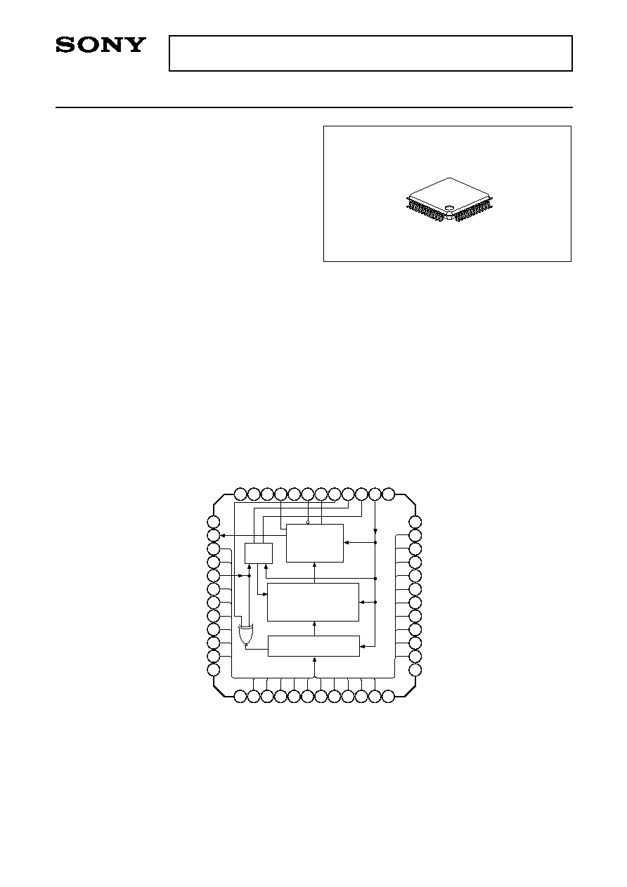
· 48-pin plastic QFP package (7mm
×
7mm)
Application
Gigabit video interface
Block Diagram and Pin Configuration
Structure
Bi-CMOS IC
Absolute Maximum Ratings
· Power supply
V
CC
4.2
V
· Operating temperature
Topr
0 to +85
°C
· Storage temperature
Tstg
65 to +150
°C
· Allowable power dissipation
P
D
333
mW
Recommended Operating Condition
Supply voltage
3.3 ± 0.3
V
1
E98Y03B03
Sony reserves the right to change products and specifications without prior notice. This information does not convey any license by
any implication or otherwise under any patents or other right. Application circuits shown, if any, are typical examples illustrating the
operation of the devices. Sony cannot assume responsibility for any problems arising out of the use of these circuits.
CXB1455R
48 pin LQFP (Plastic)
37
38
39
40
41
42
43
44
45
46
47
48
1
2
3
4
5
6
7
8
9
10 11 12
13
14
15
16
17
18
19
20
21
22
23
24
25
26
27
28
29
30
31
32
33
34
35
36
GND
CE
LPFA
LPFB
CKPOL
SDATAP
SDATAN
GNDT
REXT
V
CC
A
GNDA
V
DD
V
DD
G2
G3
G4
G5
G6
G7
B0
B1
B2
B3
GND
V
DD
R0
R1
R2
R3
R4
R5
R6
R7
G0
G1
GND
GND
REFREQ
CNTL
DE
SFTCLK
HSYNC
VSYNC
B7
B6
B5
B4
V
DD
P/S
Converter
Cable
Driver
PLL
Encoder
Fig. 1. Block Diagram and Pin Configuration

2
CXB1455R
Pin Description
Power Supply/Ground
Symbol
V
DD
GND
V
CC
A
GNDA
GNDT
12, 24, 36, 48
1, 13, 25, 37
34
35
32
Logic power supply; connected to 3.3V ± 0.3V
Logic ground; connected to 0V
Analog power supply; connected to 3.3V ± 0.3V
Analog ground; connected to 0V
Transmission ground; connected to 0V
Pin No.
Description
Digital Signal
Symbol
SFTCLK
RED (7 to 0)
GRN (7 to 0)
BLU (7 to 0)
HSYNC
VSYNC
CNTL
DE
CE
CKPOL
41
16, 17, 18, 19,
20, 21, 22, 23
6, 7, 8, 9, 10,
11, 14, 15
44, 45, 46, 47,
2, 3, 4, 5
42
43
39
40
26
29
TTL in 1
TTL in 1
TTL in 1
TTL in 1
TTL in 1
TTL in 1
TTL in 2
TTL in 2
Shift clock, for the data
fetch at rising or falling
edge
Pixel data. 1 pixel/shift
clock input.
Hsync data
Vsync data
Panel control data
Data enable
Chip enable
SFTCLK polarity
Pin No.
Type
Equivalent Circuit
Description
V
DD
TTL-IN
GND
SDATAP/N
30, 31
Tx
Serial output and Refclk
request input
V
CC
A
SDATAP
GNDT
V
DD
GND
SDATAN
GNDA
V
DD
TTL-IN
GND

3
CXB1455R
Special
REFREQ
38
TTL out
Refclk request
detection flag
V
DD
TTL-OUT
GND
Symbol
Pin No.
Equivalent Circuit
Description
Type
Symbol
REXT
33
SDATAP/N
output current
trimming.
Connect to the
external resistor.
Pin No.
Equivalent Circuit
Description
V
CC
A
GNDA
GND
REXT
V
DD
LPFA/B
27, 28
External loop filter
V
CC
A
LPFA
GNDA
GND
V
DD
LPFB

4
CXB1455R
Electrical Characteristics
Table 1. Absolute Maximum Ratings
Item
Supply voltage
TTL DC input voltage
TTL H level output current
TTL L level output current
Serial output pin voltage
Ambient temperature
Storage temperature
V
CC
V
I
_T
I
OH
_T
I
OL
_T
Vsdout
Ta
Tstg
0.3
0.5
20
0
V
CC
1.2
55
65
4.2
6.5
0
20
V
CC
+ 0.5
120
150
V
V
mA
'
mA
V
°C
°C
Under bias
Symbol
Min.
Typ.
Max.
Unit
Remarks
Table 2. Recommended Operating Conditions
Item
Supply voltage (Includes V
DD
and VccA)
Ambient temperature
V
CC
Ta
3.0
0
3.3
3.6
85
V
°C
Symbol
Min.
Typ.
Max.
Unit
Conditions
Table 3. DC Characteristics (Under the recommended operating conditions. See Table 2.)
Item
TTL High level input voltage
TTL Low level input voltage
TTL High level input current
TTL Low level input current
CE, CKPOL High level input voltage
CE, CKPOL Low level input voltage
CE, CKPOL High level input current
CE, CKPOL Low level input current
TTL High level output voltage
TTL Low level output voltage
SDATA High level output current
SDATA Low level output current
SDATA High level output voltage
SDATA Low level output voltage
Supply current
V
IH
_T
V
IL
_T
I
IH
_T
I
IL
_T
V
IH
_C
V
IL
_C
I
IH
_C
I
IL
_C
V
OH
_T
V
OL
_T
I
OH
_SD
I
OL
_SD
V
IH
_SD
V
IL
_SD
I
CC
2
0
1.0
V
CC
0.5
0
1.0
2.4
0.1
14.5
V
CC
0.55
44.0
50.0
0
15.7
61.0
71.0
5.5
0.8
1.0
5.5
0.5
1.0
0.4
+0.5
17
V
CC
0.76
77.0
92.0
V
V
µA
µA
V
V
µA
µA
V
V
mA
mA
V
V
mA
mA
V
IN
= V
CC
V
IN
= 0
V
IN
= V
CC
V
IN
= 0
I
OH
= 8mA
I
OL
= 8mA
REXT = 4.7k
Common mode
voltage
@65MHz
Symbol
Min.
Typ.
Max.
Unit
Conditions
GRAYSCALE
WORSTCASE
See Fig. 8
See Fig. 7
5
CXB1455R
Table 4. AC Characteristics (Under the recommended operating conditions. See Table 2.)
Item
TTL input rise time
TTL input fall time
Minimum SFTCLK frequency
Maximum SFTCLK frequency
SFTCLK duty factor
Pixel/Sync/Cntl setup time to
SFTCLK
Pixel/Sync/Cntl hold time to
SFTCLK
SDATA rise time
SDATA fall time
Clock mode assert time
Clock mode deassert time
Idle mode assert time
Idle mode deassert time
PLL lock-in time
Tir
Tif
Fsftclk
Dsftclk
Tsetup
Thold
Tor
Tof
TAclk
TDclk
TAidle
TDidle
Tlockin
0.7
0.7
65.0
40
2.5
2.5
200
200
50
10
150
100
0.1
5.0
5.0
25.0
60
ns
ns
MHz
MHz
%
ns
ns
ps
ps
ns
ns
ns
ns
ms
0.8 to 2.0V
2.0 to 0.8V
Vth = 1.4V
20 to 80%, C
L
= 2pF
See Fig. 2.
Symbol
Min.
Typ.
Max.
Unit
Conditions
CXB1455R
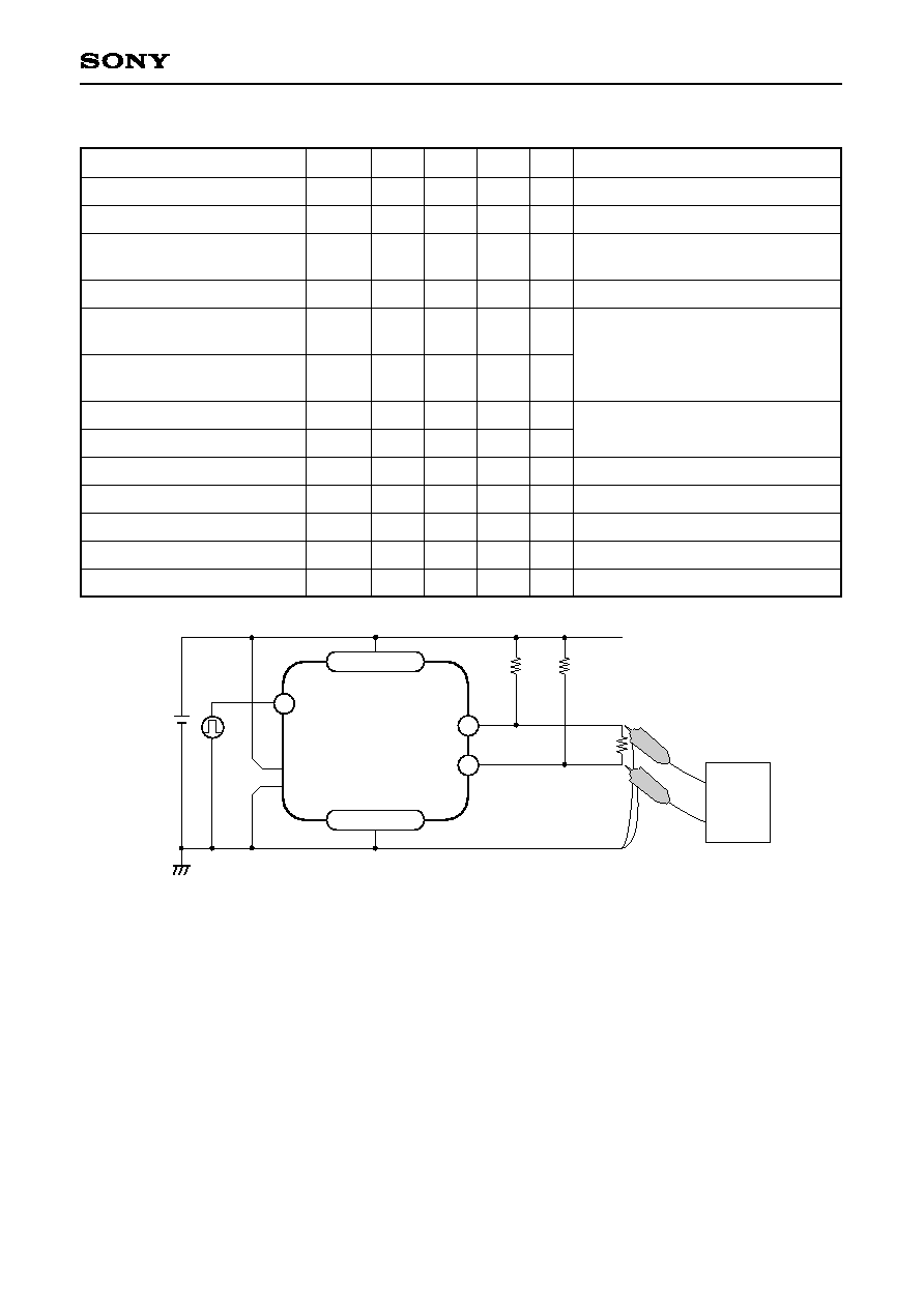
RGB, CE
VS, HS, DE, CNTL, CKPOL
FET probe
Sampling
oscillo-
scope
V
CC
51
100
V
CC
/A
TTL clock
GND/A/T
51
41
30
31
Fig. 2. SDATA waveform measurement

6
CXB1455R
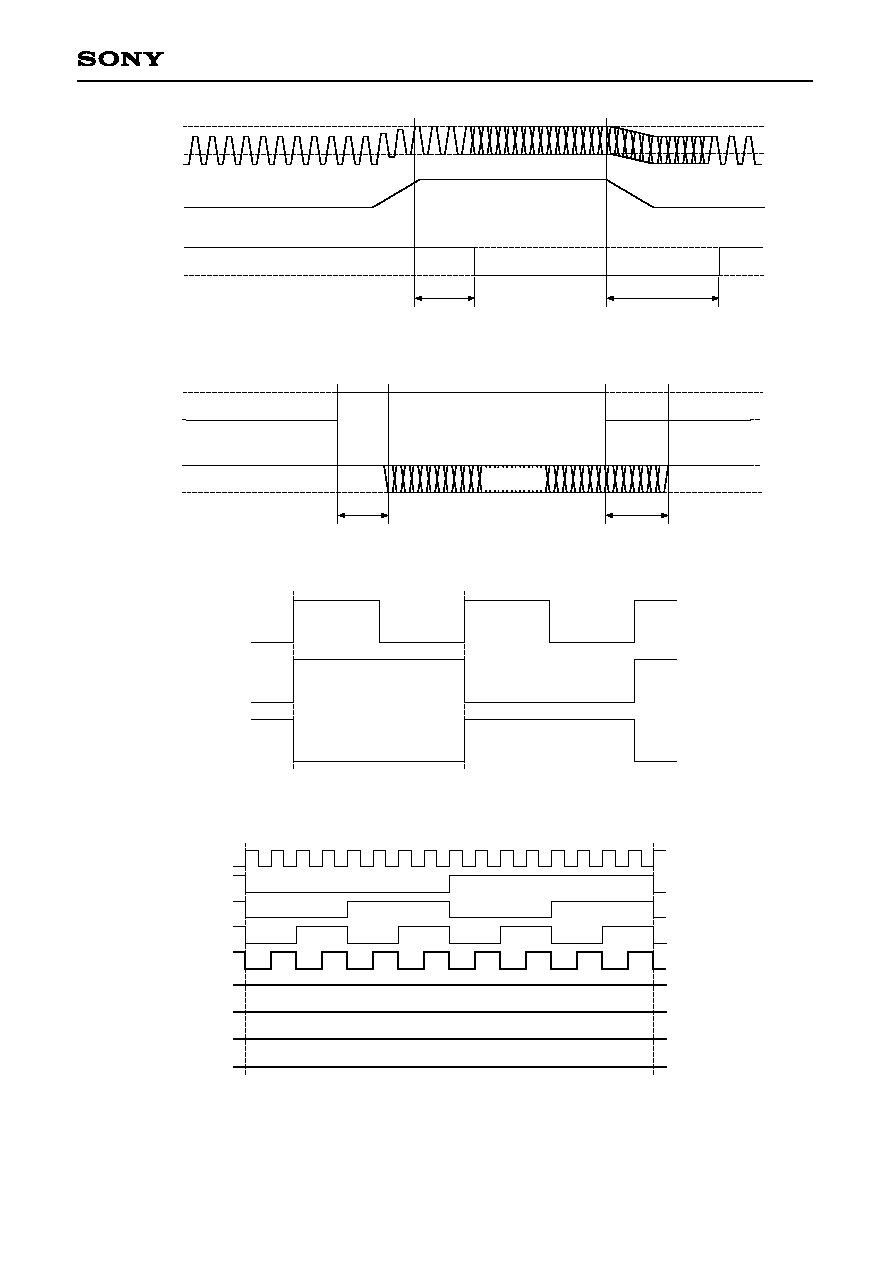
Timing Chart
SFTCLK
Tir
Tif
Tsetup
Thold
Tir
2.0V
2.0V
0.8V
0.8V
Vth
V
IL
_T
V
IH
_T
V
IL
_T
V
IH
_T
1/Fsftclk
REDxx
VSYNC
HSYNC
DE
RGB
CNTL
There must be 2 SFTCLK cycles or more left between the CNTL edge and the HSYNC, VSYNC and DE edges.
Setup/hold times are referred from
falling edge in CKPOL = GND
rising edge in CKPOL = Vcc
GRNxx
BLUxx
H/Vsync
CNTLx
Tif
Min. 2
Min. 2
Min. 2
Min. 2
Min. 2
Min. 2 (SFTCLK cycle)
Dsftclk/Fsftclk
Fig. 4. Serial output timing
Tor
80%
20%
0%
100%
SDATAP
SDATAN
Tof
Fig. 3. TTL input timing
7
CXB1455R
Fig. 5. Refclk request timing
SDATAP
SDATAN
REFREQ
Reference clock
NRZ data
REFRQ
signal from
CXB1454R
or CXB1456R
TAclk
TDclk
Fig. 6. Idle mode timing
SDATAP
SDATAN
CE
TDidle
TAidle
NRZ data
RGB
<7, 5, 3, 1>
RGB
<6, 4, 2, 0>
SFTCLK
f
f/2
f/2
Fig. 7. Worst case test pattern
f
f/16
f/8
f/4
f/2
Fix Low
Fix Low
Fix Low
Fix Low
SFTCLK
RGB <7>
RGB <6>
RGB <5>
RGB <4>
RGB <3>
RGB <2>
RGB <1>
RGB <0>
Fig. 8. 16 grayscale test pattern

8
CXB1455R
CE
SFTCLK
V
CC
When the power supply and SFTCLK stabilize
200
µ
s or more
Fig. 9. CE timing when power supply is turned ON
CE
SFTCLK
When SFTCLK does not stabilize
When SFTCLK stabilizes
200
µ
s or more
When SFTCLK stops or the frequencies of 15MHz or less and 75MHz or more are input.
Fig. 10. CE timing when SFTCLK input signal is not stabilized
CE Pin Control
The CE pin should be controlled as follows.
When the power is turned ON or SFTCLK stops, or when the SFTCLK input signal falls into the disorder while
the SFTCLK frequency is varied, the CE pin should be set to Low level and the CE pin should be set to High
level after the SFTCLK frequency stabilizes. (Figs. 9 and 10)

9
CXB1455R
Applications
The CXB1455R GVIF transmitter is applied to the digital RGB signal transmission for
P/C with LCD monitor
Video-on-demand system
Monitoring system
Graphical controller
Projector
Digital TV monitor
Automobile Navigation System
with GVIF receivers, CXB1454R/CXB1456R.
CXB1455R GVIF Transmitter
CXB1454R/CXB1456R GVIF Receiver
Parallel
to
Serial
Converter
Cable
Driver
PLL
RED (7 to 0)
GRN (7 to 0)
BLU (7 to 0)
SYNC/DE/CNTL
SHIFTCLOCK
RED (7 to 0)
GRN (7 to 0)
BLU (7 to 0)
SYNC/DE/CNTL
SHIFTCLOCK
STP or Twin axial
8
8
8
4
E
n
c
o
d
e
r
Serial
to
Parallel
Converter
Cable
Equalizer
PLL
D
e
c
o
d
e
r
8
8
8
4
Table 5. SFTCLK polarity
CKPOL
L
H
Falling edge
Rising edge
SFTCLK data sampling trigger
CKPOL Pin Control
The CKPOL pin selects the SFTCLK data sampling trigger edge. (See Table 5)
10
CXB1455R
Application Circuit
(1) Chip resistor (1%)
(2) Chip capacitor
(3) Formed by the printed circuit pattern
(L = 0.5 to 1.0mm/W = 0.5 to 1.0mm)
(4) LPF chip capacitor
(Temperature compensation type)
High: Rising edge trigger
Low: Falling edge trigger
51
(1)
680p
(4)
51
(1)
4.7k
(1)
0.1 to 0.4n (3)
0.1 to 0.4n (3)
33
µ
16V
V
CC
V
CC
V
CC
Differential cable
330
Connector
0.1
µ
(2)
7 6 5 4
RED DATA
3 2 1 0
MSB
LSB
V
CC
0.1
µ
(2)
V
CC
0.1
µ
(2)
0.1
µ
(2)
V
CC
0.1
µ
(2)
7 6 5 4
GREEN DATA
3 2 1 0
MSB
LSB
7 6 5 4
BLUE DATA
3
C
N
T
L
S
F
T
C
L
K
H
S
Y
N
C
V
S
Y
N
C
D
E
2 1 0
MSB
LSB
1
2
3
4
5
6
7
8
9
10
11
12
13
14
15
16
17
18
19
20
21
22
23
24
25
26
27
28
29
30
31
32
33
34
35
36
37
38
39
40
41
42
43
44
45
46
47
48
GND
REFREQ
CNTL
DE
SFTCLK
HSYNC
VSYNC
CXB1455R
B6
B4
B7
B5
V
CC
G
N
D
B
3
B
2
B
1
B
0
G
7
G
6
G
3
G
2
G
5
G
4
V
C
C
V
C
C
G
N
D
A
V
C
C
A
R
E
X
T
G
N
D
T
S
D
A
T
A
N
S
D
A
T
A
P
C
K
P
O
L
L
P
F
B
L
P
F
A
C
E
G
N
D
V
CC
R0
R1
R6
R7
G0
G1
R2
R3
R4
R5
GND
SW2
High: Transmission
data
Low: Standby
V
CC
330
SW1
0.01
µ
(4)
1k (1)
1k (1)
Application circuits shown are typical examples illustrating the operation of the devices. Sony cannot assume responsibility for
any problems arising out of the use of these circuits or for any infringement of third party patent and other right due to same.
11
CXB1455R
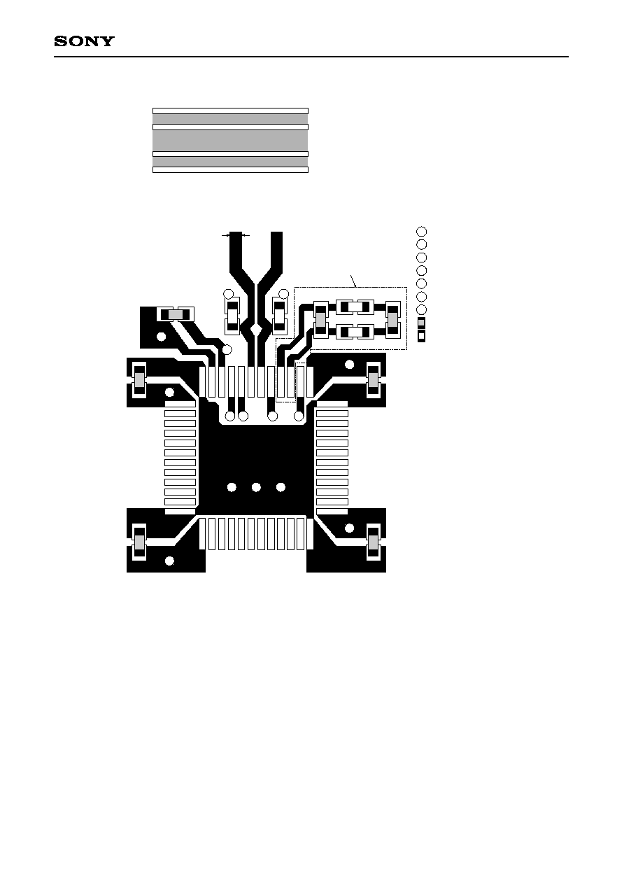
Recommended Printed Board Structure
,
,
,
,
,
,
,
,
L1: Cu plate (18
µ
m) + solder coat
I1: Fiber-glass epoxy core (0.3mm)
L2: Cu plate (36
µ
m)
I2: Fiber-glass epoxy core (0.8mm)
L3: Cu plate (36
µ
m)
I3: Fiber-glass epoxy core (0.3mm)
L4: Cu plate (18
µ
m) + solder coat
12
13
24
48
37
1
48
37
0.5mm
L2 doesn't have the plane
in this area.
Locate the bypass capacitor
(0.1
µ
F chip capacitor) as close
to the pins as possible.
,,
: Through hole to the GNDA plane (L2)
: Through hole to the GND plane (L2)
: Through hole to the VccA plane (L3)
: Through hole to the Vcc plane (L3)
: Through hole to the REXT resistor (L4)
: Through hole to the CKPOL signal (L4)
: Through hole to the CE signal (L4)
Chip capacitor
Chip resistor
R
P
C
G
A
E
T
GND
REFREQ
CNTL
DE
SFTCLK
HSYNC
VSYNC
BLU <7>
BLU <6>
BLU <5>
BLU <4>
V
CC
G
N
D
B
L
U
<
3
>
B
L
U
<
2
>
B
L
U
<
1
>
B
L
U
<
0
>
G
R
N
<
7
>
G
R
N
<
6
>
G
R
N
<
5
>
G
R
N
<
4
>
G
R
N
<
3
>
G
R
N
<
2
>
V
C
C
V
C
C
G
N
D
A
V
C
C
A
R
E
X
T
G
N
D
T
S
D
A
T
A
N
S
D
A
T
A
P
C
K
P
O
L
L
P
F
B
L
P
F
A
C
E
G
N
D
V
CC
RED <0>
RED <1>
RED <2>
RED <3>
RED <4>
RED <5>
RED <6>
RED <7>
GRN <0>
GRN <1>
GND
G
P
T
T
T
R
C
,,
,,
,,
,,
,
,,
,,
,,
,,
E
E
A
G
G
E
G
G
Microstrip Line
The microstrip line with the characteristic impedance of 50
should be used to connect the LSI transmission
signal pin SDATAP/N to the connector foot printer as GVIF transmits the high-speed digital signal with the
maximum speed of 2Gb/s. The optimal line can be made by forming 0.5mm pattern on L1. (See the board
structure shown below.) The line lengths should be the same and the through hole should be not used.
Normally, L2 should be the mat GND.
Termination Elements
Locate the 51
termination resistors as close to the LSI as possible.
Filter Device and Reference Resistor
The capacitor and resistor connected to LPFA/B and REXT are the filter and the reference resistor. Locate
them as close to the LSI as possible. Decrease the parasitic capacitance by removing the L2 GND plane
under these elements and wiring.
Recommended Printed Circuit Board Pattern
Example of power supply and special signal routing

12
CXB1455R
By-pass Capacitor
Locate a 0.1 µF chip capacitor as close to the pin as possible as shown in the Recommended Circuit Diagram.
Notes on Transmission System Configuration
The GVIF uses termination on both the transmitting and receiving ends, built-in equalizers, small amplitude
differential signals, etc. in order to more easily resolve problems such as signal reflectance, signal attenuation
and EMI which interfere with high-speed data transmission.
However, a number of cautions must be observed over the entire transmission system shown in the figure
below in order to completely resolve these problems.
Tx
LSI
Rx
LSI
Tx
termination
50
Tx
termination
100
Microstrip
line
(50
)
Microstrip
line
(50
)
Foot
print
Foot
print
Cable
(diff. 100
)
Connector
Connector
The transmission system has the following four requirements.
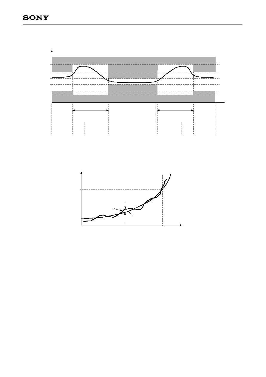
· Impedance matching shall be excellent. (Reflectance shall be low.)
A differential impedance that falls within the template shown on the following page is recommended.
· Attenuation shall be low and regular.
For the CXB1454R (built-in equalizer)
Attenuation of 15 dB (conforming to root f attenuation) @ 1 GHz or less is recommended.
See the following page.
For the CXB1456R (no equalizer)
Attenuation of 6 dB @ 1 GHz or less is recommended.
· Differential signal POS/NEG skew shall be small.
12% or less during the time for one bit is recommended.
160 ps @ VGA, 100 ps @ SVGA, 60 ps @ XGA
· EMI characteristics shall be excellent.
The following measures are effective for satisfying these requirements.
· Use a low attenuation, low skew differential cable with excellent impedance accuracy.
A cable with a two-core coaxial (shielded twisted pair) structure is recommended.
· Use low reflectance connectors.
· Take care for the connector pin assignment.
Select pins so that there is no interference with other signals and so that the positive and negative signal
wiring are the same length on the board.
· Use a cable with a double shielded structure.
13
CXB1455R
Recommended Transmission Path : Differential impedance template
150
Zo
(
)
110
106
94
90
75
Microstrip
line
Microstrip
line
Foot
print
Foot
print
Connector
< 500ps
< 500ps
Connector
Cable
Recommended Transmission Path : Attennation Characteristics
Loss
< 15dB
Measured curve
Fitting curve
2dB
1GHz
Frequency

14
CXB1455R
1.95Gbps SDATAP output waveform
100mV/div
100ps/div
ATTEN 10dB
RL 0dBm
CENTER 65.00MHz
RBW 100kHz
SPAN 10.00MHz
SWP 50ms
VBW 100kHz
10dB/
SFCLK jitter tolerance: Example of power spectrum which can be used for transmission
D
REF LVL
0dBm
15
CXB1455R
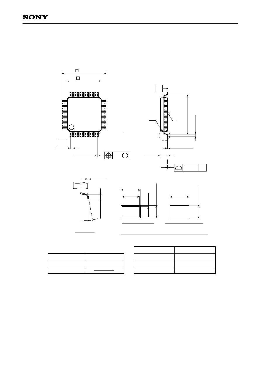
Package Outline
Unit: mm
SONY CODE
EIAJ CODE
JEDEC CODE
PACKAGE MATERIAL
LEAD TREATMENT
LEAD MATERIAL
PACKAGE MASS
EPOXY RESIN
PLATING
42/COPPER ALLOY
PACKAGE STRUCTURE
48PIN LQFP (PLASTIC)
9.0 ± 0.2
7.0 ± 0.1
1
12
13
24
25
36
37
48
(0.22)
0.18 0.03
+ 0.08
0.2g
LQFP-48P-L01
LQFP048-P-0707
(
8
.
0
)
0
.
5
±
0
.
2
0.127 0.02
+ 0.05
A
1.5 0.1
+ 0.2
0.1
SOLDER/PALLADIUM
NOTE: Dimension "
" does not include mold protrusion.
0.1 ± 0.1
0
.
5
±
0
.
2
0° to 10°
DETAIL A
0.13 M
0.5
S
S
B
DETAIL B:SOLDER
(0.18)
(
0
.
1
2
7
)
DETAIL B:PALLADIUM
0
.
1
2
7
±
0
.
0
4
0.18 0.03
+ 0.08
0
.
1
2
7
0
.
0
2
+
0
.
0
5
0.18 ± 0.03
NOTE : PALLADIUM PLATING
This product uses S-PdPPF (Sony Spec.-Palladium Pre-Plated Lead Frame).
Sony Corporation