Digital CCD Camera Head Amplifier
Description
The CXA2056Q is a bipolar IC developed as a
head amplifier for digital CCD cameras. This IC
provides the following functions: correlated double
sampling, AGC for the CCD signal, GCA for the low-
band chroma signal, AMP for high-band chroma and
line signals, A/D sample and hold, blanking, A/D
reference voltage, and an output driver.
Features
Ě High sensitivity made possible by a high-gain AGC
amplifier
Ě Blanking function provided for the purpose of
calibrating the CCD output signal black level
Ě Regulator output pin provided for A/D converter
reference voltage
Ě Built-in GCA and AMP for amplifying video signals
(chroma and line signals) from external sources
Ě Built-in sample-and-hold circuits for camera signals
required by external A/D converters
Absolute Maximum Ratings
Ě Supply voltage
V
CC
11
V
Ě Operating temperature
Topr
ş20 to +75
░C
Ě Storage temperature
Tstg
ş65 to +150
░C
Ě Allowable power dissipation
P
D
1160
mW
Operating Conditions
Supply voltage
V
CC
1, 2, 3
3 to 3.3
V
Applications
Digital CCD cameras
Structure
Bipolar silicon monolithic IC
ş 1 ş
E96119A8X-PS
Sony reserves the right to change products and specifications without prior notice. This information does not convey any license by
any implication or otherwise under any patents or other right. Application circuits shown, if any, are typical examples illustrating the
operation of the devices. Sony cannot assume responsibility for any problems arising out of the use of these circuits.
CXA2056Q
32 pin QFP (Plastic)
ş 2 ş
CXA2056Q
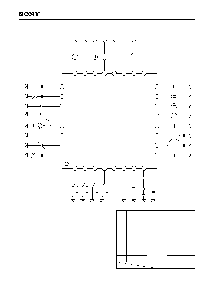
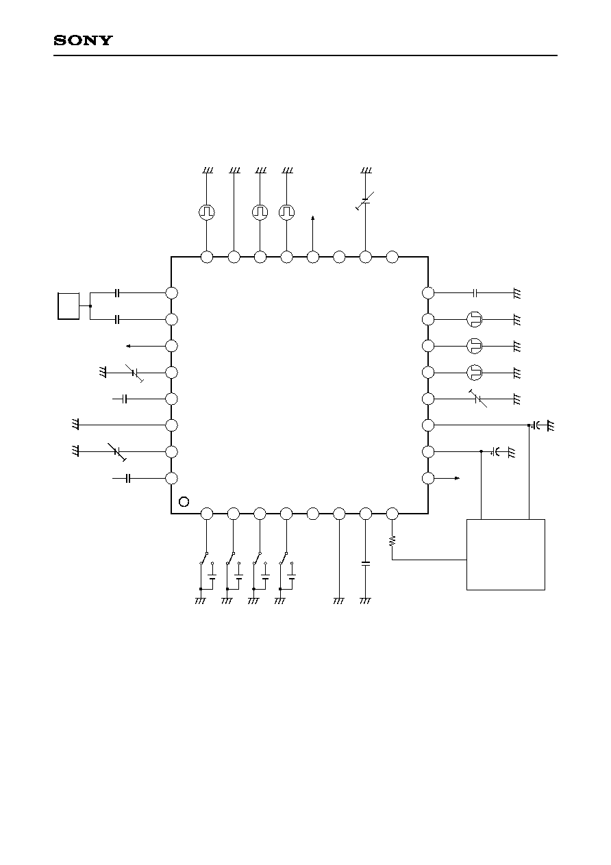
Block Diagram and Pin Configuration
DC
SHIFT
BUF
SH1
SH2
SH3
VIDC
SHIFT
V
REF
DMSW1
DMSW2
V
SI
CH
SW
CAM
SH
OBSW
V
S2
V
CENT
V
CENT
MODE CONTROL
&
POWER SAVE CONTROL
LOSW
V
B
V
RT
OFFSET
V
RB
CVSW
V
CENT
V
B
V
B
BLK SW
26
27
28
29
30
31
32
25
9
10
11
12
13
14
15
16
2
3
4
5
6
7
8
1
17
18
19
20
21
22
23
24
PIN
PBRFC
DIN
V
CC
2
ICONT
LIN/CH
GND2
RFCONT
AGCCLP
V
CC
3
CLPOB
XRS
PBLK
OFFSET
VRT
VRB
M
O
D
E
1
D
R
V
O
U
T
M
O
D
E
2
M
O
D
E
3
P
S
N
.
C
G
N
D
3
L
O
U
T
C
L
P
C
L
P
D
M
N
.
C
G
N
D
1
S
H
D
S
H
P
V
C
C
1
C
C
D
L
E
V
E
L
A
G
C
C
O
N
T
VISW
LISW
1
2
3
CDS
CLP1
CDS
CLP2
LIN
CLP
LIN
CH AMP
CL
GCA
CAM
DRV
VIDEO
DRV
LOUT
CLP
V
RT
DRV
V
RB
DRV
A
G
C
C
L
P
AGC
ş 3 ş
CXA2056Q
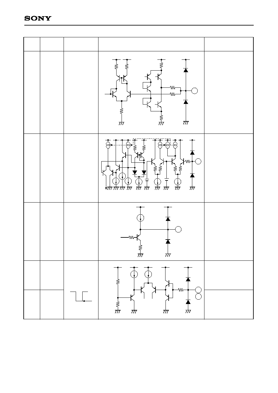
Pin Description
(V
CC
1, 2, 3 = 3V)
Pin
No.
Symbol
Pin voltage
Equivalent circuit
Description
1
MODE1
Camera and video
signal selector.
Composite video
signal and high-band
chroma/low-band
chroma signal
selector of the video
signal.
For details on the
selection conditions
for each mode, refer
to the diagram of the
Electrical
Characteristics
Measurement Circuit.
2
MODE2
3
MODE3
4
PS
Power saving mode.
5
17
N.C
No connection;
normally ground.
6
23
30
GND3
GND1
GND2
Ground.
7
LOUTCLP
Capacitor connection
for LOUTCLP which
clamps the output
minimum level in
modes which pass
the composite video
signal.
(Recommended
value: 0.1ÁF)
VTH = 1.5V
GND
Approx. 1.1V
145
75k
50k
50k
10ÁA
2
3
4
1
1.5V
7
2ÁA
100ÁA
100ÁA
38k
1k
90k
22k
12k
145
1.1V

ş 4 ş
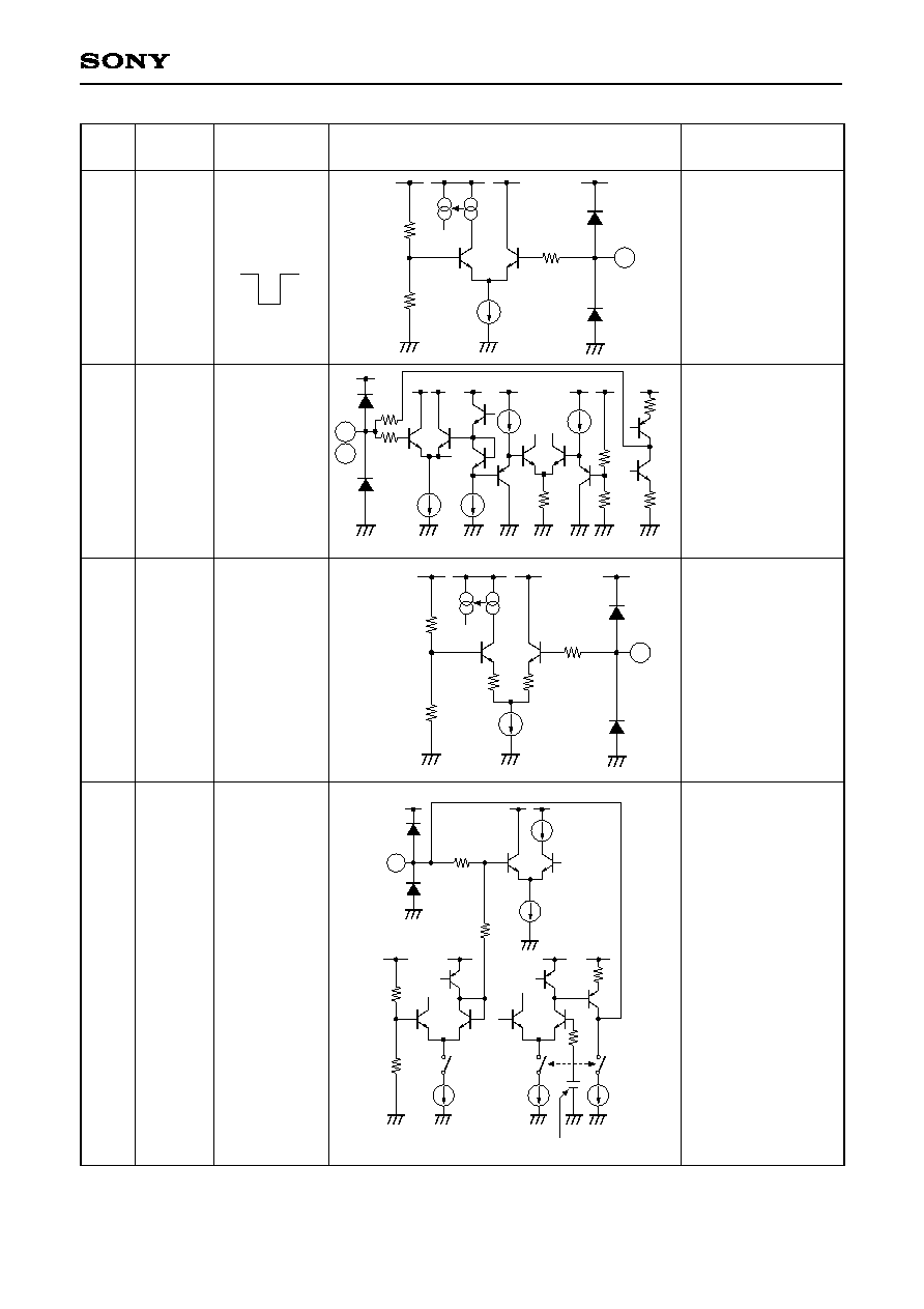
CXA2056Q
Pin
No.
Symbol
Pin voltage
Equivalent circuit
Description
8
DRVOUT
Driver output for A/D
converter capable of
DC coupling.
Dynamic range
= 1Vp-p
Ě Camera
mode (CAM)
V
RB
to V
RB
+
100mV
Ě Composite
video mode
(LIN)
V
RB
+ 50mV
= approx.
1.4V
Ě Chroma
mode
(CH, CL)
Center
voltage =
(V
RT
ş V
RB
)/2
= approx.
1.85V
10
VRB
1.35V regulator
output.
Be sure to decouple
this pin near the IC
pins to prevent the
oscillation and external
noise when this pin is
not used.
(Recommended
capacitor value: 4.7ÁF)
9
20
27
V
CC
3
V
CC
1
V
CC
2
Power supply.
V
CC
1.35V
2.35V
11
VRT
2.35V regulator
output.
Be sure to decouple
this pin near the IC
pins to prevent the
oscillation and external
noise when this pin is
not used.
(Recommended
capacitor value: 4.7ÁF)
100ÁA
5090
4072
509
30k
10p
1.4
1.85V
30k
SW3
SW1
SW2
2.4mA
CAM signal
VIDEO signal
48
50ÁA
SW1
145
I
CONT
3.2 to 6.4mA
200ÁA
50ÁA
25ÁA
25ÁA
2k
I
OFFSET
0 to
50ÁA
SW1
V
RT
= 2.35V
V
RB
= 1.35V
8
SW1 SW2
Mode
1
0
0
0
1
1
SW3
0
1
0
CAM
LIN
CH, CL
0: Open
1: Closed
200
30k
16.5k
13.5k
145
1.35V
110ÁA
10
30k
6.5k
23.5k
145
2.35V
220Á
11
55Á
55Á
200
ş 5 ş
CXA2056Q
Pin
No.
Symbol
Pin voltage
Equivalent circuit
Description
12
OFFSET
Controls the output
offset during camera
mode.
When 3V: V
RB
When 1.5V:
V
RB
+ 100mV
When 0V
(preset mode):
V
RB
+ 35mV
1.5 to 3V
&
0V
2k
30k
30k
50k
50k
1.5k
3k
25k
V
RB
145
50ÁA
50ÁA
50ÁA
12
1.85V
13
PBLK
Camera signal
preblanking pulse
input.
Active when Low only
during camera mode.
Calibrates the black
level of the AGC output
waveform.
When PBLK is Low,
the DRVOUT potential
is forced to V
RB
.
VTH = 1.85V
13
145
50ÁA
30k
30k
1.85V
30k
14
XRS
Camera signal
sample-and-hold
pulse input.
VTH = 0.68V
24k
7k
0.68V
770ÁA
40ÁA
97Á
145
14
15
CLPOB
Clamp pulse used to
clamp the optical
black portion of the
camera signal after it
passes through the
AGC amplifier.
VTH = 1.5V
145
50ÁA
30k
30k
1.5V
30k
15
Active: Low
Sampling
Active: Low
ş 6 ş
CXA2056Q
Pin
No.
Symbol
Pin voltage
Equivalent circuit
Description
16
AGCCLP
AGC clamp capacitor.
(Recommended
value: 0.1ÁF)
Approx. 1.3V
18
AGCCONT
AGC gain control.
When 1.5V: ş1dB
(Minimum gain)
When 3.0V: +31.5dB
(Maximum gain)
1.5 to 3.0V
50k
145
145
5k
5k
3k
3k
16
145
18
200ÁA
3.4k
3.4k
200ÁA
2.14V
100ÁA
300ÁA
300ÁA
100ÁA
2.29V
I
CONT
3.4k
3.4k
3.3k
3.3k
19
CCDLEVEL
Enables monitoring of
the SH3 output
camera signal.
DIN input
CCD signal
black level:
approx. 2.2V
21
SHP
Preset level sample-
and-hold pulse input.
22
SHD
Data level sample-
and-hold pulse input.
VTH = 0.65V
500
19
340
100ÁA
36k
10k
0.65V
365ÁA
20ÁA
145
21
22
Sampling
ş 7 ş
CXA2056Q
Pin
No.
Symbol
Pin voltage
Equivalent circuit
Description
24
CLPDM
Clamp pulse used to
clamp the dummy
pixel portion of the
input CCD signal.
VTH = 1.5V
145
50ÁA
30k
30k
1.5V
24
25
26
28
PIN
DIN
ICONT
CCD signal input.
DRVOUT output
waveform rise time
control.
When 1.5V:
Maximum rise time
When 3V:
Minimum rise time
Black level:
approx. 2.1V
1.5 to 3V
145
145
200ÁA
50ÁA
23k
26
25
7k
14k
2k
2k
15ÁA
15ÁA
145
100ÁA
15k
45k
28
6k
6k
2.25V
29
LIN/CH
Common input for the
composite video
signal (LIN) and high-
band chroma signal
(CH).
Clamp
potential
during
LIN mode:
approx. 1.46V
During
CH mode:
approx. 1.85V
145
50ÁA
25ÁA
200ÁA
11.5k
18.5k
1.85V
CH mode
100ÁA
LIN mode
2ÁA
10k
30k
V
RB
+ 50mV
29
54k
Active: Low

ş 8 ş
CXA2056Q
Pin
No.
Symbol
Pin voltage
Equivalent circuit
Description
31
RFCONT
Gain control for the
low-band chroma
signal (CL).
When 0.3V: ş4dB
(Minimum gain)
When 2.7V: +12.5dB
(Maximum gain)
0.3 to 2.7V
54k
145
42k
27k
27k
31
32
PBRFC
Low-band chroma
signal (CL) input.
Approx. 1.9V
32
145
200ÁA
100ÁA
7.8k
2k
58k
10k
10k
200ÁA
38k
1.9V
22k
25ÁA
2.9V
ş 9 ş
CXA2056Q
Electrical Characteristics
(Ta=25░C, V
CC
1, 2, 3 = 3V)
Camera
mode
LINE mode
CH mode
CL mode
PS mode
Maximum
gain
Minimum
gain
Range of gain
variance
Dynamic
range
maximum
Dynamic
range
typical
Offset high
Offset low
Offset
preset
V
RT
DC
level
V
RB
DC
level
V
RT
ş V
RB
Offset
LIN mode
gain
CH mode
gain
CL mode
maximum gain
CL mode
minimum gain
Dynamic
range
I
DC
I
DL
I
DCH
I
PCL
I
DP
A CONT
max.
A CONT
min.
AGC G
AGCmax.
D
AGC
TYP
.
D
CAOF
high
CAOF
low
CAOF
pre
VRTO
VRBO
VR
BLKOF
LIN G
CH G
RF
CONmax.
RF
CONmin.
SH3 D
AGCCONT = 1.5V, open between V
RT
and V
RB
MODE1 = 3V, MODE2 = 0V
MODE3 = 0V, PS = 3V, I
CONT
= 3V
Open between V
RT
and V
RB
MODE1 = 0V, MODE2 = 0V,
MODE3 = 0V, PS = 3V
Open between V
RT
and V
RB
MODE1 = 0V, MODE2 = 3V,
MODE3 = 3V, PS = 3V
RFCONT = 0.3V, open between V
RT
and V
RB
MODE1 = 0V, MODE2 = 3V,
MODE3 = 0V, PS = 3V
PS = 0V
DIN = 1Ás, 20mVp-p pulse
AGCCONT = 3V, I
CONT
= 3V
DIN = 1Ás, 500mVp-p pulse
AGCCONT = 1.5V, I
CONT
= 3V
A CON max. ş A CON min.
AGCCONT = 3V
DRVOUT output signal at saturation level
AGCCONT = 2V
DRVOUT output signal at saturation level
Camera mode
OFFSET = 1.5V
Camera mode
OFFSET = 3.0V
Camera mode
OFFSET = 0V
With a 400
load
With a 400
load
With a 400
load
BLKOF (PBLK = 3V) ş BLKOF (PBLK = 0V)
LIN/CH = 15kHz, 500mVp-p,
Sine wave + offset voltage
LIN/CH = 3MHz, 500mVp-p, sine wave
RFCONT = 2.7V
15kHz 80mVp-p sine wave
RFCONT = 0.3V
15kHz 500mVp-p sine wave
DIN = 1Ás, 1Vp-p pulse
Item
Symbol
Conditions
Min.
Typ.
Max. Unit
Current
consump-
tion
AGC
DRV
mA
dB
mV
mV
mV
mV
dB
REF
BLK
AMP
GCA
30
10
9
9
2
28.5
--
27.1
800
900
80
--
25
2300
1300
950
--10
2.5
2.5
9.5
--
600
41.0
13.9
12.2
12.2
3.4
31.3
ş0.8
32.1
895
955
98
2
34
2342
1359
983
9
3.43
3.18
12.7
ş4.0
815
53
19
17
17
6
--
1.4
--
--
--
--
5
40
2400
1400
1050
23
4.5
4.5
--
ş2.5
--
mV
SH3
ş 10 ş
CXA2056Q
Electrical Characteristics Measurement Circuit
M
O
D
E
1
L
GND
M
O
D
E
2
L
H
H
V1
3V
GND
V2
3V
M
O
D
E
3
L
H
V3
3V
GND
P
S
L
H
V4
3V
GND
SW2
SW1
SW4
SW3
GND
GND
GND
G
N
D
3
L
O
U
T
C
L
P
D
R
V
O
U
T
V5
1.85V
C5
0.1Á
R1
10k
GND
C6
70pF
R2
22
G
N
D
PL5
XRS
G
N
D
PL4
CLPOB
C7
0.1ÁF
G
N
D
G
N
D
VRT
G
N
D
VRB
C9
4.7ÁF
R3
400
SW6
ON
OFF
C8
4.7ÁF
G
N
D
OFFSET
V6
0 to 3V
G
N
D
V
CC
3
V
CC
3
3V
V
CC
2
G
N
D
V
CC
2
3V
C4
1ÁF
G
N
D
PIN
C3
1ÁF
G
N
D
DIN
AC
V8
C2
0.047ÁF
G
N
D
PBRFC
AC
V13
G
N
D
V12
0.3 to 2.7V
RFCONT
C1
0.1ÁF
G
N
D
LIN/
CH
AC
V11
SW5
V10
0 to 3V
ON
OFF
GND
C
L
P
D
M
PL1
GND
G
N
D
1
GND
S
H
D
PL2
GND
S
H
P
PL3
GND
V
C
C
1
GND
A
G
C
C
O
N
T
C
C
D
L
E
V
E
L
N
.
C
V7
1.5 to 3V
V
CC
1
3V
AGCCLP
ICONT
G
N
D
GND2
9
10
11
12
13
14
15
16
17
18
19
20
21
22
23
24
25
26
27
28
29
30
31
32
2
3
4
5
6
7
8
1
N
.
C
G
N
D
V9
1.5 to 3V
G
N
D
PL6
PBLK
SW1
L
H
H
L
H
L
L
SW2
L
L
L
L
H
H
H
SW3
H
L
H
L
L
L
H
SW5 SW4
MODE
OFF
ON
OFF
H
CAM
LIN
CL
CH
L
POWER SAVE

ş 11 ş
CXA2056Q
Measurement Timing Chart
Different for each test
Different for each test
2.5V
GND
2.5V
GND
2.5V
GND
2.5V
GND
1H
2Ás
2Ás
1H
Equivalent to CCD
signal black level
PL4 (CLPOB)
PL1 (CLPDM)
PL6 (PBLK)
V8 (DIN)
V11 (CH)
V13 (PBRFC)
V10 + V11 (LIN)
PL2 (SHD)
PL3 (SHP)
PL5 (XRS)
1H
ş 12 ş
CXA2056Q
Application Circuit
M
O
D
E
1
GND
M
O
D
E
2
3V
GND
3V
M
O
D
E
3
3V
GND
P
S
3V
GND
GND
GND
G
N
D
3
L
O
U
T
C
L
P
D
R
V
O
U
T
0.1ÁF
22
N
.
C
G
N
D
PBLK
G
N
D
XRS
G
N
D
CLPOB
0.1ÁF
G
N
D
G
N
D
VRT
G
N
D
VRB
4.7ÁF
4.7ÁF
G
N
D
OFFSET
0 to 3V
V
CC
3
V
CC
2
PIN
1ÁF
DIN
0.047ÁF
PBRFC
G
N
D
0.3 to 2.7V
RFCONT
0.1ÁF
LIN/CH
GND
C
L
P
D
M
GND
G
N
D
1
GND
S
H
D
GND
S
H
P
V
C
C
1
GND
A
G
C
C
O
N
T
C
C
D
L
E
V
E
L
N
.
C
V
AGCCONT
1.5 to 3V
AGCCLP
ICONT
G
N
D
GND2
9
10
11
12
13
14
15
16
17
18
19
20
21
22
23
24
25
26
27
28
29
30
31
32
2
3
4
5
6
7
8
1
1ÁF
CCD
V
CC
LIN/CH
PBRFC
V
CC
V
RB
V
RT
A/D IN
A/D
CLPDM
SHD
SHP
V
CC
P
B
L
K
X
R
S
C
L
P
O
B
V
RFCONT
V
ICONT
G
N
D
1.5 to 3V
V
OFFSET
Application circuits shown are typical examples illustrating the operation of the devices. Sony cannot assume responsibility for
any problems arising out of the use of these circuits or for any infringement of third party patent and other right due to same.

ş 13 ş
CXA2056Q
Description of Operation
Refer to the Block Diagram.
1. Camera signal processing system
Process the video signal processing pins as follows only in camera mode.
<7> LOUTCLP ... Connect to GND.
<29> LIN/CH
... Connect to GND.
<31> RFCONT ... Connect to GND via the capacitor (approx. 0.01ÁF).
<32> PBRFC
... Connect to GND.
Operating conditions
The camera signal processing system operates when PS is High, MODE1 is Low, MODE2 is Low and MODE3
is High, or when PS is High, MODE1 is High, MODE2 is Low and MODE3 is Low.
Camera signal processing system timing chart (when V
CC
= 3V)
PBLK
(10Á during the idle
transfer interval)
Sig interval
OPB interval
Idle transfer
interval
Sig interval
Precharge level
Signal level
2.1V
2.1V
[
1]
2Ás
0.65V
Black level
Basic black
level
2Ás
0.65V
10Ás
1.35V
Approx. V
RB
+ 35mV when OFFSET = 0V
Approx. V
RB
+ 100mV when OFFSET = 1.5V
Approx. V
RB
when OFFSET = 3V
CCD output
SHP
SHD
SH1 output
SH2 output
SH3 output
CLPDM
(2Á dummy bit portion during
the idle transfer interval)
XRS
CLPOB
(2Á during the OPB
interval)
CAMSH
output
BLK SW output
CAM DRVOUT output
AGC output
Î
(ş N)
SH3 output
ş SH2 output
[
2]
[
3]
[
4]
[
5]

ş 14 ş
CXA2056Q
CDS (SH1, SH2, SH3):
The CCD signal from the CCD image sensor is input to PIN and DIN where correlated double sampling (CDS)
is performed by SH1, SH2 and SH3. The precharge level of the CCD output signal is sampled, held and output
by the SH2 output, and the signal level is sampled, held and output by the SH3 output. SH1 and SH2 are the
sample-and-hold circuits for the pre-charge level; SH3 is the sample-and-hold circuit for the signal level.
CDSCLP 1, 2:
CDSCLP1 and 2 stabilize the input signal DC level, clamp (CLPDM) the input signal during the idle transfer
interval for the purpose of eliminating the AGC input offset, and adjust the DC level ([
1], [
2]) of SH2 and SH3
in line with V
REF
. CDSCLP1 is the clamp circuit for the precharge level, and CDSCLP2 is the clamp circuit for
the signal level.
AGC:
AGC is the gain control amplifier for the camera signal.
The gain can be varied from ş1 to +31dB by adjusting the AGCCONT voltage control V
AGCCONT
from 1.5 to
3.0V.
CAM SH:
CAM SH is the sample-and-hold circuit for the camera signal processing system; it synchronizes the data read-
in timing for the external A/D.
Sampling is possible according to the approximately 10ns sampling pulse width input to XRS.
AGCCLP:
The basic black level is set ([*3]) by clamping the AGC output waveform with the CLPOB clock during the OPB
interval. When PBLK is High and CLPOB is Low, the clamping circuit operates, adjusting the AGCCLP current
so that the DRVOUT potential equals the OFFSET potential (which is determined by the voltage applied to the
OFFSET pin), thus setting the AGCCLP potential. The AGCCLP capacitance is connected to the AGCCLP pin.
DC SHIFT:
This circuit functions when AGCCLP operates, following the AGCCLP potential and forcing a DC shift of the
AGC output waveform OPB interval to the basic black level. When AGCCLP is not operating, the basic black
level is maintained at its previous setting.
BLK SW:
The black level is calibrated by blanking the black level signal of the AGC output waveform so that it does not
fall below the basic black level and replacing the DC potential with V
RB
. ([
4])
The signal is blanked when PBLK is low.
CVSW:
When the MODE1, 2, 3 and PS pin voltages are set so that the camera signal processing system operates,
CVSW conducts the CAMDRV output (camera signal) into the DRVOUT. In addition, when these voltages are
set so that the video signal processing system operates, CVSW conducts the VIDEODRV output (video signal)
into the DRVOUT.

ş 15 ş
CXA2056Q
OFFSET:
OFFSET controls the CAMDRV output waveform black level offset.
In the camera signal processing system camera mode, the OFFSET pin is enabled, permitting adjustment of
the offset for the [OFFSET] and DRVOUT camera signals. ([
5]) The voltage controlled by OFFSET is output
as the CAMDRV output DC offset via AGCLP, DCSHIFT, CAMSH, and BLKSW.
When the OFFSET voltage is 1.5 to 3.0V, DRVOUT DC can vary in a linear fashion from V
RB
+ 100mV to V
RB
.
In addition, when the OFFSET voltage is 0V, DRVOUT DC is preset to V
RB
+ 35mV.
CAMDRV:
CAMDRV operates in the camera signal processing system mode, driving the external A/D. The current that
flows to the last-stage amplifier in CAMDRV is controlled by applying voltage to the ICONT pin, making it
possible to adjust the rise time of the output waveform, which affects the external A/D load capacitance. The
variable range is 1.5 to 3V, with 1.5V yielding the maximum and 3V yielding the minimum. The optimum rise
time for the external A/D input capacitance can be selected.
V
RT
DRV, V
RB
DRV:
These are the external A/D reference voltage drivers. These circuits are connected to A/D V
RT
and V
RB
,
supplying 2.35V and 1.35V, respectively, when V
CC
is 3V. The IC's internal primary voltage is also generated
on the basis of the V
RT
and V
RB
voltages. (V
RB
, V
B
, and V
CENT
)
MODE CONTROL & POWER SAVE CONTROL:
This block selects the mode governing the operation of the camera signal system and the video signal system
through the selection of High and Low potential for the MODE1, 2, 3, and PS pins. The PS pin is the POWER
SAVE pin; the power saving function operates when this pin is Low.
2. Video signal processing system
Operating conditions
The video signal processing system has three modes: LIN signal mode, CH signal mode and CL signal mode.
The video signal processing system operates in LIN signal mode when PS is High, MODE1 is High, MODE2 is
Low and MODE3 is High, or when PS is High, MODE1 is Low, MODE 2 is Low and MODE3 is Low.
The video signal processing system operates in CH signal mode when PS is High, MODE1 is Low, MODE2 is
High and MODE3 is High.
The video signal processing system operates in CL signal mode when PS is High, MODE1 is Low, MODE2 is
High and MODE3 is Low, or when PS is High, MODE1 is Low, MODE2 is High and MODE3 is High.
Video signal processing system timing chart (when V
CC
= 3V)
LIN mode
1.46V
1.4V
LIN/CH input
Ě LIN CHAMP output (3.5dB)
Ě DRVOUT output

ş 16 ş
CXA2056Q
LIN signal mode
In LIN signal mode, LINSW and LOSW close, VISW is set to "1" and the video signal passes through CVSW.
In addition, LINCHAMP, LINCLP, LOUTCLP, VIDC SHIFT, and VIDEO DRV all operate.
LINCLP:
LINCLP is an input clamp circuit that clamps the video composite signal sync level.
The video composite signal is input to LIN/CH pin. LINCLP expands the input dynamic range, and sync tip
clamps the input signal at V
B
(= 1.4V) to allow full input. The input level and frequency are respectively
571mVp-p (Max.) and DC is up to 7MHz.
LINCHAMP:
LINCHAMP amplifies the LIN signal and the CH (high-band chroma) signal; the gain is fixed at 3.5dB.
VISW:
VISW switches the LIN signal, the CH (high-band chroma) signal, and the CL (low-band chroma) signal. The
signals are switched according to the mode selection.
LOUTCLP:
LOUTCLP is an output clamp circuit that clamps the sync level of the video composite signal that is output
from VIDEO DRV.
Because the VIDEO DRV output signal is fully input to the external A/D, the clamp level is set to V
B
(= 1.4V).
If the sync level of the signal output from VIDEO DRV drops below V
B
, LOUTCLP operates: the LOUTCLP
current flows so that the sync level equals V
B
, and the LOUTCLP potential is set. A clamping capacitor is
connected to the LOUTCLP pin.
VIDC SHIFT:
VIDC SHIFT functions when LOUTCLP operates, following the LOUTCLP potential and forcing a DC shift of
the VIDEO output signal sync level to V
B
.
VIDEO DRV:
VIDEO DRV outputs the video signal (LIN, CH, CL) to the external A/D in video signal processing mode.

ş 17 ş
CXA2056Q
CH (high-band chroma) signal mode
In CH mode, CHSW closes, VISW is set to "2" and the video signal passes through CVSW. In addition,
LINCHAMP and VIDEO DRV operate.
V
S1
:
The video high-band chroma signal is input to the LIN/CH pin. V
S1
expands the input dynamic range and sets a
center DC bias so that the center potential of the SIN signal is 1.85V to allow full input. The input level and
frequency of the CH signal are respectively 470mVp-p (Max.) and from 1 to 7MHz.
V
CENT
:
V
CENT
is a DC bias circuit that operates when the CH signal is output to VIDEO DRV. The DC bias potential is
generated from V
RT
and V
RB
, and is set to 1.85V.
CH mode
1.85V
LIN/CH input
Ě LINCH AMP output
(3.5dB)
Ě DRVOUT output
1.85V

ş 18 ş
CXA2056Q
CL (low-band chroma) signal mode
In CL mode, VISW is set to "3" and the video signal passes through CVSW. In addition, CLGCA and VIDEO
DRV operate.
V
S2
:
The video low-band chroma signal is input to the PBRFC pin. V
S2
expands the input dynamic range and sets a
center DC bias so that the center potential of the SIN signal is 1.9V to allow full input. The input level and
frequency of the CH signal are respectively 1490mVp-p (Max.) and DC is up to 1.5MHz.
CLGCA:
The CLGCA amplifier controls the gain of the CL signal input to the PBRFC pin. The gain can be varied from
ş4 to +12.5dB by adjusting the RFCONT voltage from 0.3 to 2.7V. The phase of the CLGCA output waveform
is reversed in DRVOUT.
V
CENT
:
V
CENT
is a DC bias circuit that operates when the CL signal is output to VIDEO DRV. The DC bias potential is
generated from V
RT
and V
RB
, and is set to 1.85V.
CL mode
1.9V
PBRFC input
Ě CLGCA output
(ş4 to +12.5dB)
Ě DRVOUT output
1.85V
ş 19 ş
CXA2056Q
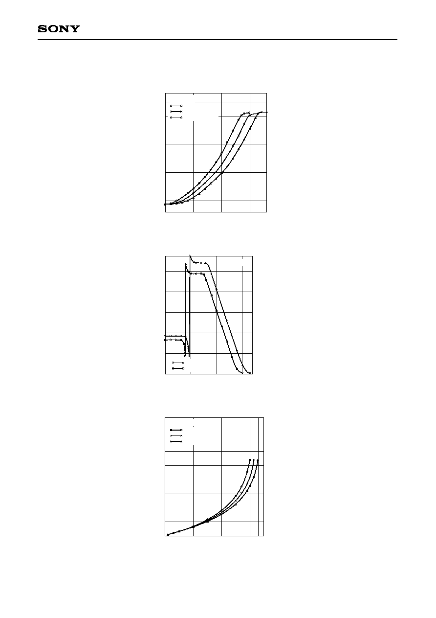
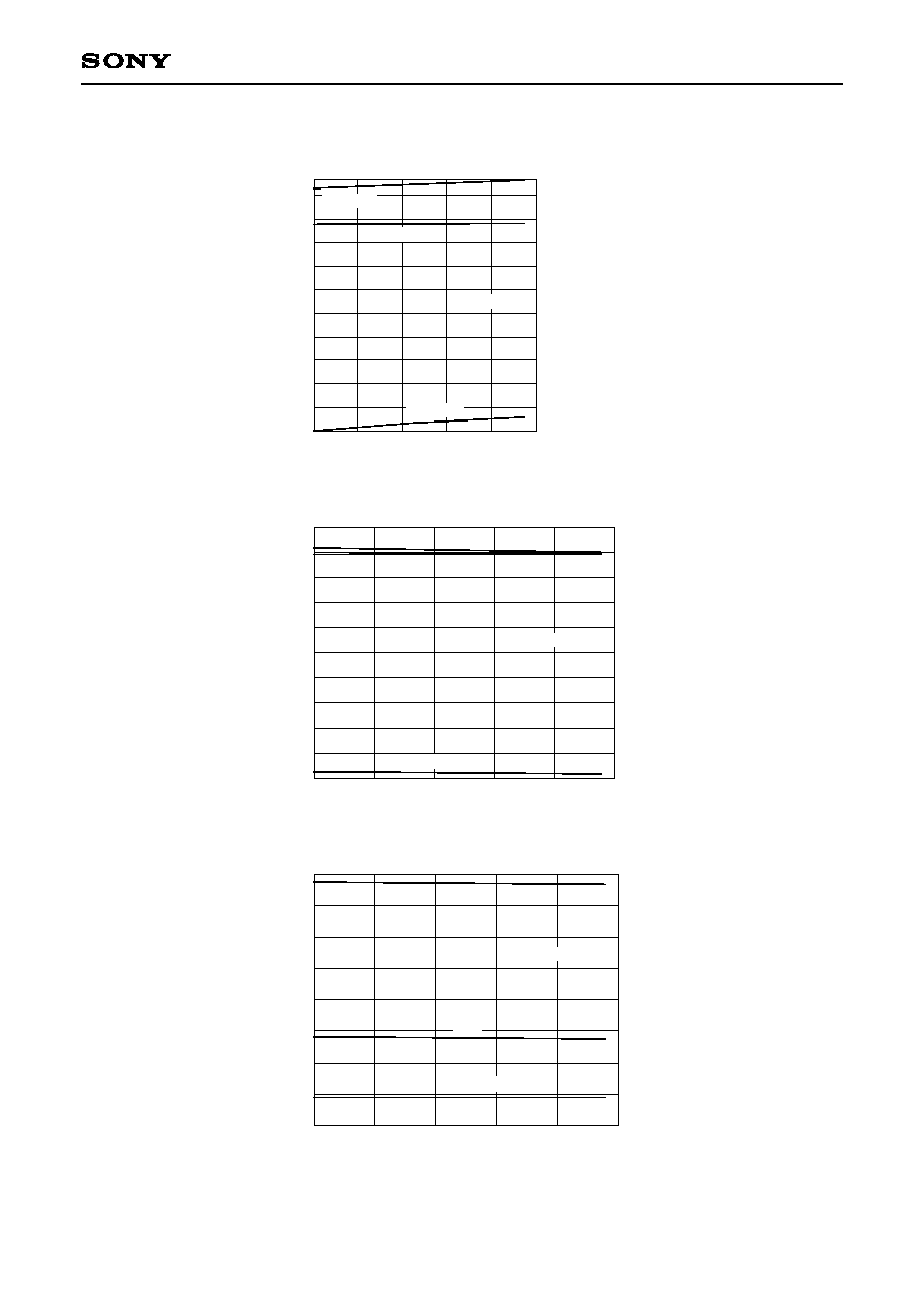
Example of Representative Characteristics
CAM mode AGCCONT control supply voltage characteristics
V
AGCCONT
vs. Gain
V
AGCCONT
[V]
1.5
2.0
2.5
3.0
3.3
0
10
20
30
35
G
a
i
n
[
d
B
]
Tc = 27░C
V
CC
= 3V
V
CC
= 3.15V
V
CC
= 3.3V
CAM mode OFFSET control supply voltage characteristics
V
OFFSET
vs. OFFSET
V
OFFSET
[V]
0
1.0
2.0
3.0 3.3
20
40
60
80
100
O
F
F
S
E
T
[
m
V
]
Tc = 27░C
V
CC
= 3.3V
V
CC
= 3V
115
CL mode RFGCA gain control supply voltage characteristics
V
RFCONT
vs. Gain
V
RFCONT
[V]
0
1.0
2.0
3.0 3.3
ş5
0
10
20
25
G
a
i
n
[
d
B
]
Tc = 27░C
V
CC
= 3V
V
CC
= 3.15V
V
CC
= 3.3V
ş4
(V
RB
=) 0
ş 20 ş
CXA2056Q
CAM mode AGCCONT control temperature characteristics
AGCCONT vs. Gain
AGCCONT [V]
1.5
2.0
2.5
3.0
0
10
20
30
35
G
a
i
n
[
d
B
]
V
CC
= 3.0V
CAM mode OFFSET control temperature characteristics
V
OFFSET
vs. OFFSET
V
OFFSET
[V]
0
1.0
2.0
3.0
50
100
O
F
F
S
E
T
[
m
V
]
V
CC
= 3.0V
150
Tc = ş20░C
Tc = +27░C
Tc = +75░C
CL mode RFGCA gain control temperature characteristics
V
RFCONT
vs. Gain
V
RFCONT
[V]
0
1.0
2.0
3.0
2.7
ş5
0
10
20
25
G
a
i
n
[
d
B
]
0.3
V
CC
= 3V
Tc = ş20░C
Tc = +27░C
Tc = +75░C
(V
RB
=) 0
ş4
Tc = ş20░C
Tc = +27░C
Tc = +75░C
ş 21 ş
CXA2056Q
CAM mode maximum signal amplitude
temperature characteristics (Min. gain)
Tc vs. Vout
Tc [░C]
ş20
0.6
V
o
u
t
[
V
p
-
p
]
0.7
0.8
0
50
100
0.53
V
CC
= 3.0V, AGCCONT = 1.5V
Input amplitude DIN =
Input amplitude DIN =
Input amplitude DIN =
Input amplitude DIN =
Input amplitude DIN =
870mVp-p
800mVp-p
750mVp-p
700mVp-p
600mVp-p
0.9
DIN = 870mVp-p
DIN = 800mVp-p
DIN = 750mVp-p
DIN = 700mVp-p
DIN = 600mVp-p
LIN, CH mode LINCHAMP gain
temperature characteristics
Tc vs. Gain
Tc [░C]
ş20
G
a
i
n
[
d
B
]
3
3.5
4
0
75
V
CC
= 3.0V
LIN mode
CH mode
V
CC
[V]
3
G
a
i
n
[
d
B
]
3
3.15
3.3
3.5
4
LIN, CH mode LINCHAMP gain supply
voltage characteristics
V
CC
vs. Gain
Tc = 27░C
CH mode
LIN mode
CAM mode maximum signal amplitude
temperature characteristics (Max. gain)
Tc vs. Vout
Tc [░C]
ş20
0.8
V
o
u
t
[
V
p
-
p
]
0.9
1.0
0
50
100
0.75
V
CC
= 3.0V, AGCCONT = 3.0V
Input amplitude DIN =
Input amplitude DIN =
Input amplitude DIN =
28mVp-p
24mVp-p
21mVp-p
30.99dB 30.99dB
30.76dB
31.41dB 31.41dB
31.03dB
31.45dB 31.45dB
31.12dB
DIN = 28mVp-p
30.99 dB
+0
ş0.23
DIN = 24mVp-p
31.41 dB
+0
ş0.38
DIN = 21mVp-p
31.45 dB
+0
ş0.33
Gain temperature
characteristics from
ş20 to +100░C
ş 22 ş
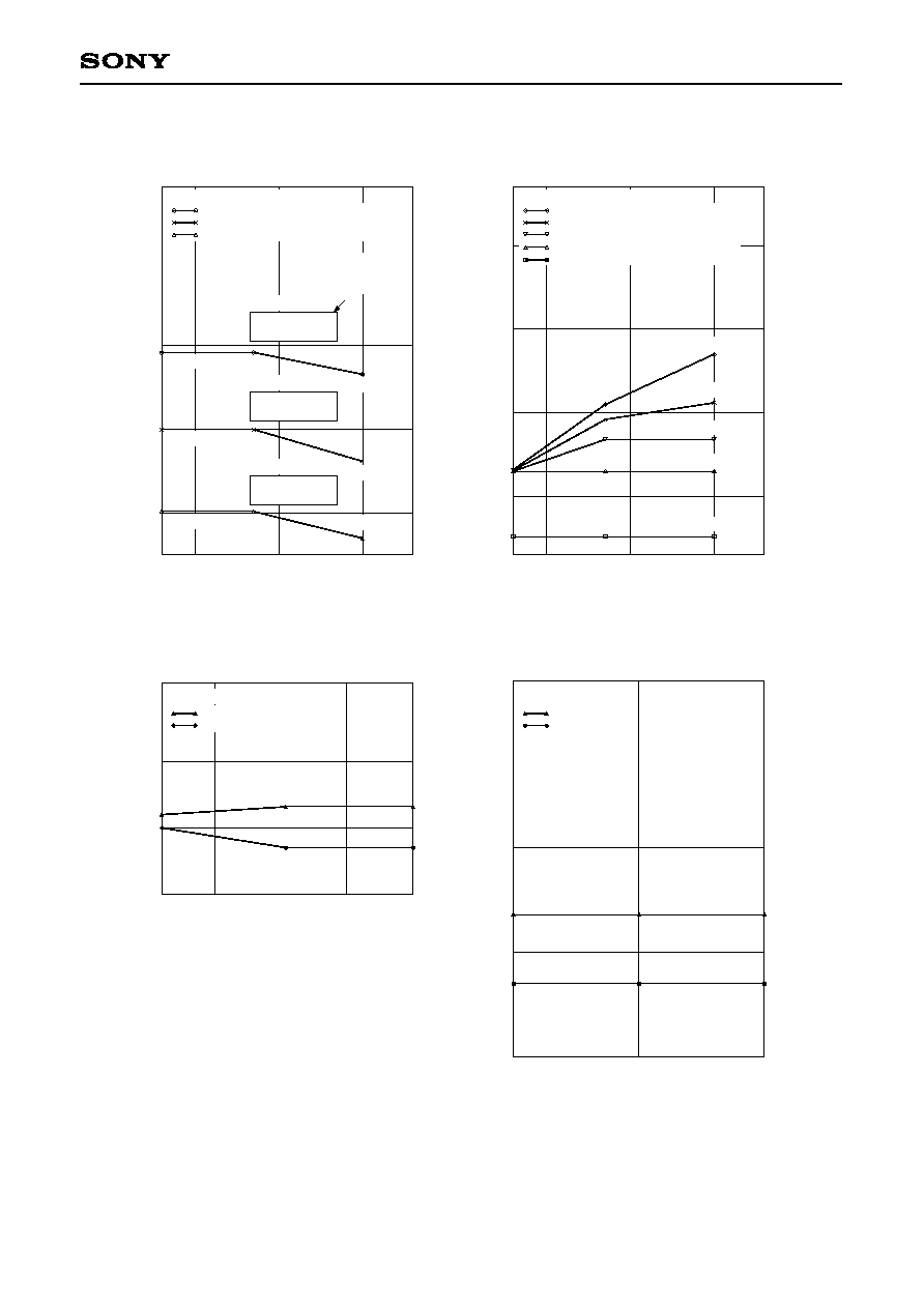
CXA2056Q
CH, LIN, CL mode DRVOUT output DC voltage
temperature characteristics
V
CC
= 3.0V
Tc [░C]
ş20
D
C
O
U
T
1.4
80
0
20
40
60
1.9
1.85
1.8
1.75
1.7
1.65
1.6
1.55
1.5
1.45
CL mode
CH mode
LIN mode
Tc [░C]
ş20
D
C
I
N
1.4
80
0
20
40
60
1.9
1.85
1.8
1.75
1.7
1.65
1.6
1.55
1.5
1.45
CL mode
CH mode
LIN mode
V
CC
= 3.0V
Tc vs. DCIN
V
RT
, V
RB
, V
RT
ş V
RB
temperature characteristics
Tc vs. V
RT
, V
RB
, V
RT
ş V
RB
V
CC
= 3.0V
Tc [░C]
ş20
V
R
T
,
V
R
B
,
V
R
T
ş
V
R
B
[
V
]
0.8
80
0
20
40
60
2.4
2.2
2.0
1.8
1.6
1.4
1.2
1.0
V
RT
V
RB
V
RT
ş V
RB
CH, LIN, CL mode input pin DC voltage
temperature characteristics
Tc vs. DCOUT
ş 23 ş
CXA2056Q
CL mode 2nd/3rd harmonic distortion
temperature characteristics (Max. gain)
V
CC
= 3.0V, RFCONT = 2.7V
f = 700kHz
Tc [░C]
ş20
2
n
d
/
3
r
d
H
a
r
m
o
n
i
c
D
i
s
t
o
r
t
i
o
n
[
d
B
]
ş80
80
0
20
40
60
ş75
ş70
ş65
ş60
ş55
ş50
ş45
ş40
ş35
ş30
2nd: out = 0.75Vp-p
3rd: out = 0.75Vp-p
3rd: out = 0.3Vp-p
2nd: out = 0.3Vp-p
LIN mode 2nd/3rd harmonic distortion
temperature characteristics
V
CC
= 3.0V
f = 5MHz
Tc [░C]
ş20
2
n
d
/
3
r
d
H
a
r
m
o
n
i
c
D
i
s
t
o
r
t
i
o
n
[
d
B
]
ş80
80
0
20
40
60
ş75
ş70
ş65
ş60
ş55
ş50
ş45
ş40
ş35
ş30
2nd: out = 0.9Vp-p
3rd: out = 0.9Vp-p
3rd: out = 0.75Vp-p
2nd: out = 0.75Vp-p
CH mode 2nd/3rd harmonic distortion
temperature characteristics
V
CC
= 3.0V
f = 5MHz
Tc [░C]
ş20
2
n
d
/
3
r
d
H
a
r
m
o
n
i
c
D
i
s
t
o
r
t
i
o
n
[
d
B
]
ş80
80
0
20
40
60
ş75
ş70
ş65
ş60
ş55
ş50
ş45
ş40
ş35
ş30
2nd: out = 0.75Vp-p
3rd: out = 0.75Vp-p
3rd: out = 0.9Vp-p
2nd: out = 0.9Vp-p
CL mode 2nd/3rd harmonic distortion
temperature characteristics (Min. gain)
Tc [░C]
ş20
2
n
d
/
3
r
d
H
a
r
m
o
n
i
c
D
i
s
t
o
r
t
i
o
n
[
d
B
]
ş80
80
0
20
40
60
ş75
ş70
ş65
ş60
ş55
ş50
ş45
ş40
ş35
ş30
2nd: out = 0.75Vp-p
3rd: out = 0.75Vp-p
2nd: out = 0.3Vp-p
3rd: out = 0.3Vp-p
V
CC
= 3.0V, RFCONT = 0.3V
f = 700kHz
Tc vs. 2nd/3rd harmonic distortion
Tc vs. 2nd/3rd harmonic distortion
Tc vs. 2nd/3rd harmonic distortion
Tc vs. 2nd/3rd harmonic distortion
ş 24 ş
CXA2056Q
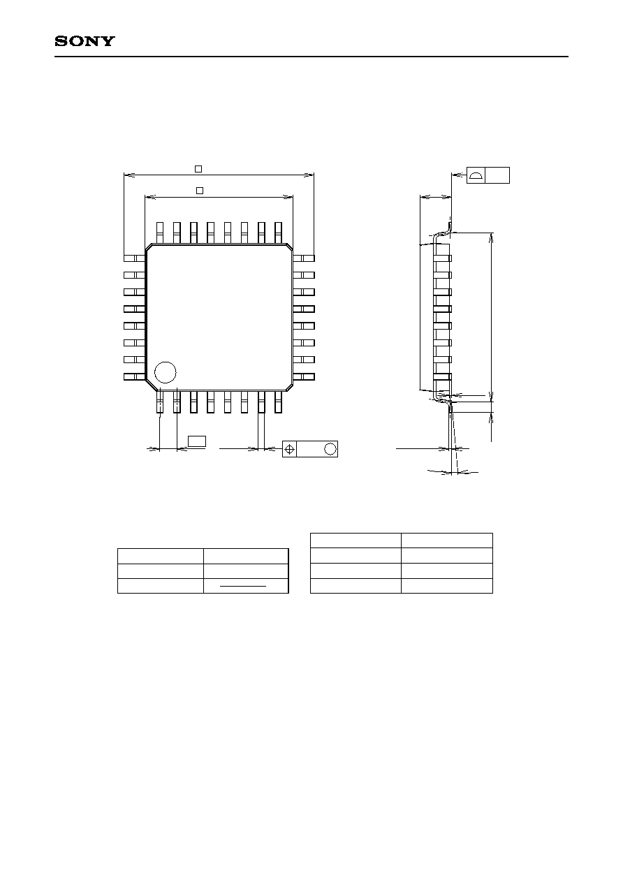
Package Outline
Unit: mm
SONY CODE
EIAJ CODE
JEDEC CODE
PACKAGE MATERIAL
LEAD TREATMENT
LEAD MATERIAL
PACKAGE MASS
EPOXY RESIN
SOLDER PLATING
42 ALLOY
32PIN QFP (PLASTIC)
9.0 ▒ 0.2
7.0 ş 0.1
1.5 ş 0.15
(
8
.
0
)
0.1 ş 0.1
+ 0.2
+ 0.35
+ 0.3
0
.
5
0
0.127 ş 0.05
+ 0.1
0░ to 10░
0.8
0.3 ş 0.1
+ 0.15
1
8
9
32
16
17
24
25
M
0.24
0.2g
QFP-32P-L01
QFP032-P-0707
0.1