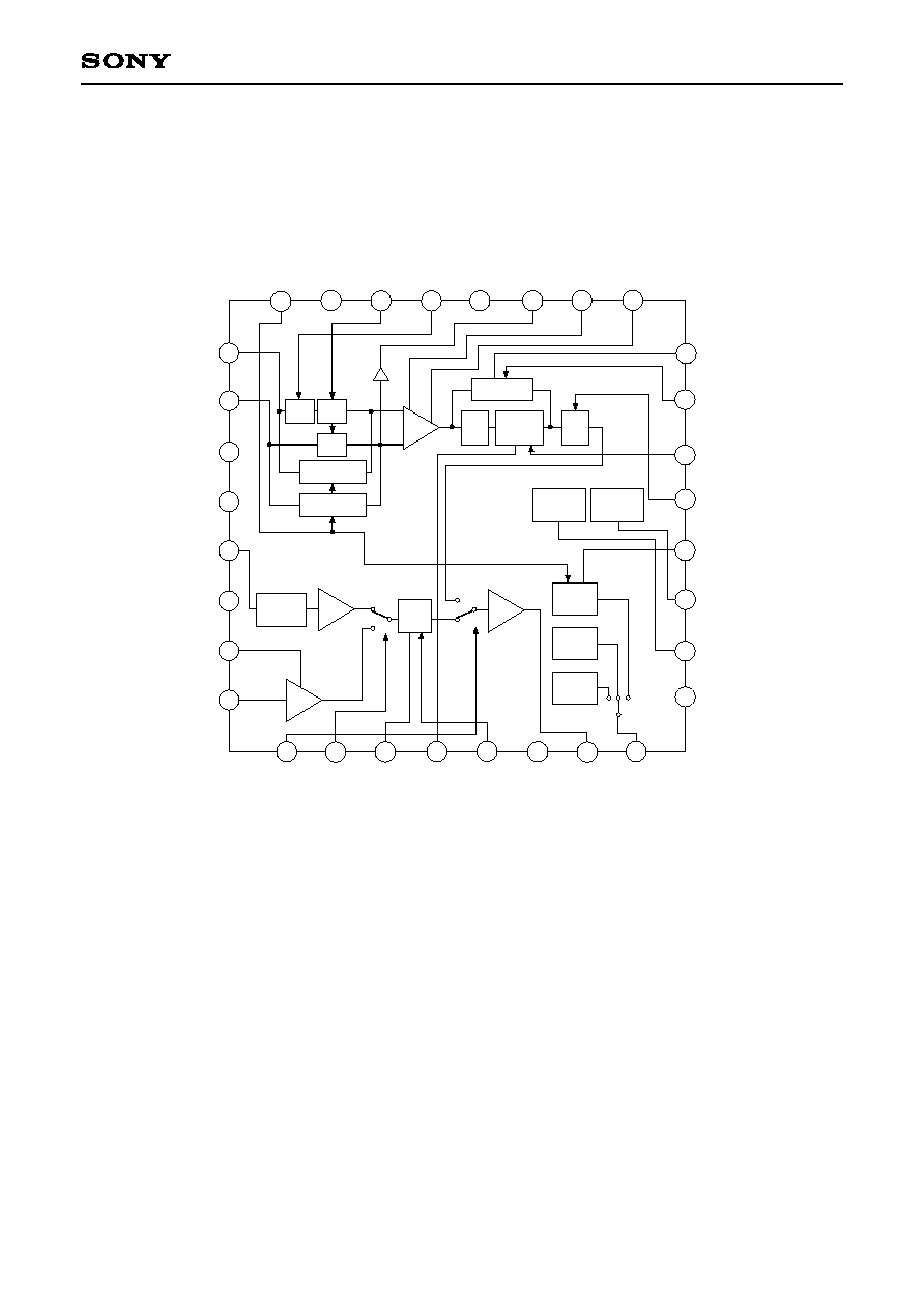
Head Amplifier for Digital CCD Cameras
Description
The CXA1690Q is a bipolar IC developed as a
head amplifier for digital CCD cameras. The
CXA1690Q provides the following functions:
correlated double sampling, AGC for CCD signals,
GCA for chroma signals, GCA for line signals,
sample and hold for A/D converters, blanking, and
reference voltage output/output driver for A/D
converters.
Features
· Permits higher sensitivity with a high-gain AGC
amplifier
· Blanking function for the purpose of calibrating the
deviation in black levels of the CCD output signals
· Permits output offset adjustment
· Provides a regulator output pin for the reference
voltage for A/D converters
· Built-in GCA that amplifies video signals (chroma
and line signals) from an external source
· Built-in sample-and-hold circuits (for both camera
signals and video signals) required by external A/D
converters
Absolute Maximum Ratings
· Supply voltage
V
CC
14
V
· Operating temperature
Topr
20 to +75
°C
· Storage temperature
Tstg
65 to +150
°C
· Allowable power dissipation
P
D
460
mW
Operating Conditions
Supply voltage
V
CC1
,
2
,
3
4.5 to 5
V
1
E93X02A8X-PS
Sony reserves the right to change products and specifications without prior notice. This information does not convey any license by
any implication or otherwise under any patents or other right. Application circuits shown, if any, are typical examples illustrating the
operation of the devices. Sony cannot assume responsibility for any problems arising out of the use of these circuits.
CXA1690Q
32 pin QFP (Plastic)
Structure
Bipolar silicon monolithic IC
Applications
Digital CCD cameras
3
CXA1690Q
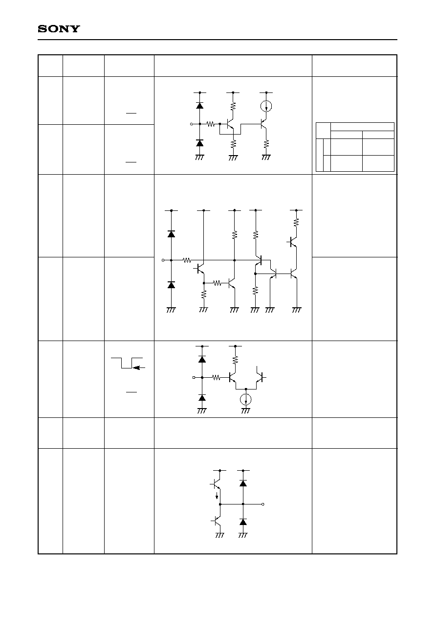
Pin Description
(Vcc = 4.5V)
1k
46µA
127
30k
1k
1k
127
50k
7k
3k
2.4k
V
RT
100
100
127
2mA
Typ.
14mA
Typ.
Pin
No.
Symbol
Pin voltage
Equivalent circuit
Description
1
CAM
VIDEO
H: Vcc
L: GND
18
V
TH
=
50
Vcc
Switches between CAM
mode for the camera
signal system and PB
and LIN modes for the
video signal system.
2
PB REC
H: Vcc
L: GND
18
V
TH
=
50
Vcc
3
VSHI
1.4V
This pin adjusts the
slew rate when the
video sample-and-hold
circuit (VISH) built into
the CXA1690 is
sampling. Normally
used open.
R = 1K: approx. +6dB;
R = 5K: approx. 6dB
4
CSHI
1.4V
This pin adjusts the
slew rate when the
camera sample-and-
hold circuit (CAMSH)
built into the CXA1690
is sampling. Normally
used open.
R = 1K: approx. +6dB;
R = 5K: approx. 6dB
5
VSHP
Sampling
18
V
TH
=
50
Vcc
Pulse input for VISH.
6
23
30
GND3
GND1
GND2
GND
Driver GND.
Camera signal GND.
Video signal GND.
7
DRVOUT
Camera
system CAM
mode black
level: 1.3V
Video
system LIN
mode black
level: 1.4V
Video
system RF
mode DC
level: 2.2V
Driver output.
Standard D range.
Camera system
signal: 870mVp-p
Video system PB RFC
signal: 500mVp-p
Video system LIN
signal: 1.4Vp-p
PB REC
CAM VIDEO
High
Low
Video system
PB mode
Video system
PB mode
Camera system
CAM mode
Video system
LIN mode
High
Low
4
CXA1690Q
127
50µ
400µ
157µ
78µ
86µ
LIN mode
switch
PB mode
switch
1k
CAM mode
switch
127
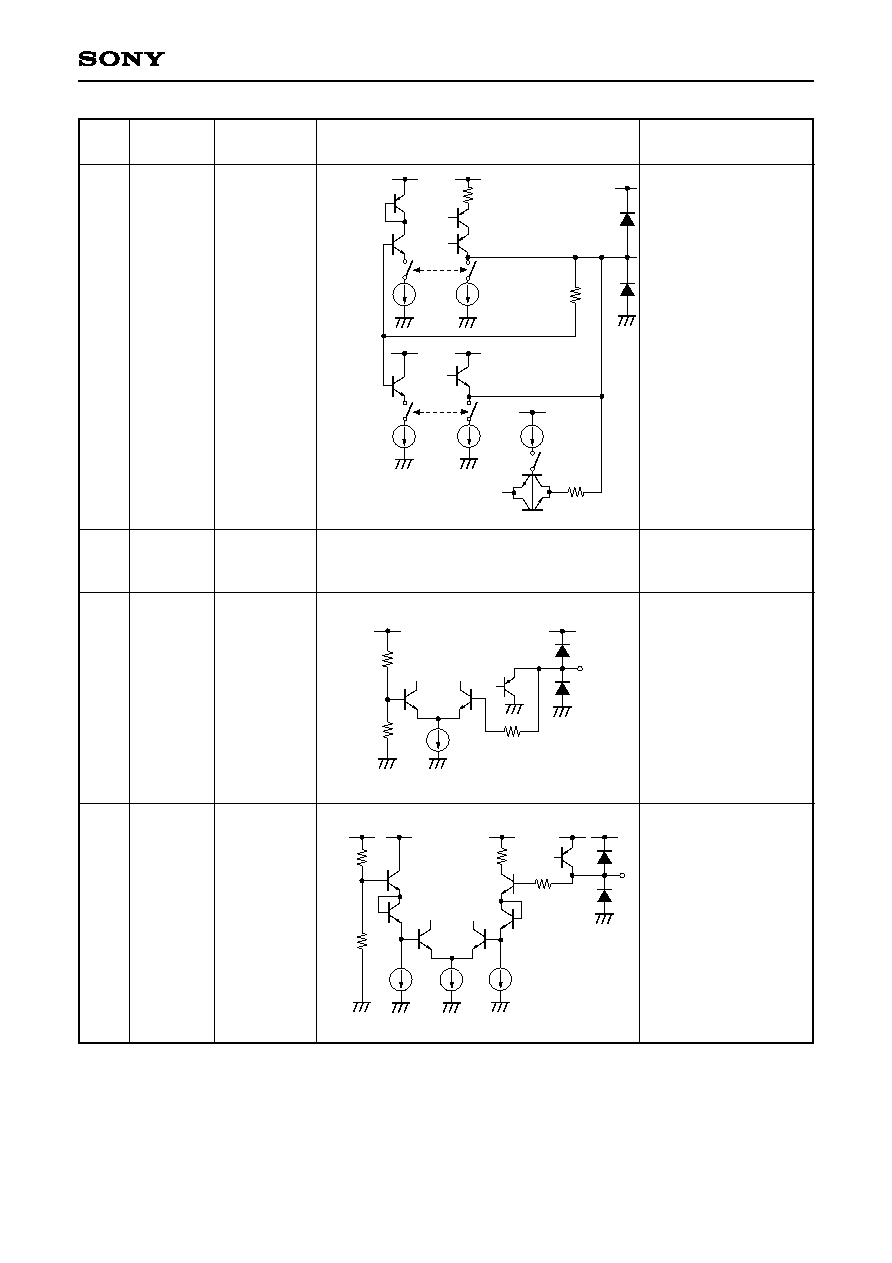
Pin
No.
Symbol
Pin voltage
Equivalent circuit
Description
8
CLPDRV
Camera
system CAM
mode black
level: 2V
Video
system LIN
mode clamp
level: 2V
Video
system PB
mode DC
level: 3V
Clamps and outputs
the DRVOUT (Pin 7)
output signal.
The switch for each
mode is closed and the
clamp potentials
applied to this pin by
selecting CAMVIDEO
(Pin 1) or PBRFC (Pin
2).
9
20
27
Vcc3
Vcc1
Vcc2
Vcc
Driver V
CC
.
Camera signal V
CC
.
Video signal V
CC
.
11
V
RT
3.88V
4V regulator output.
Be sure to decouple this
pin near the IC pins to
prevent the oscillation
and external noise when
this pin is not used.
(Recommended
capacitor value: 4.7µF)
10
V
RB
2.02V
2V regulator output
V
RB
V
RT
load:
160
or greater.
Be sure to decouple this
pin near the IC pins to
prevent the oscillation
and external noise when
this pin is not used.
(Recommended
capacitor value: 4.7µF)
91µA
16k
13k
6k
91µA
4k
25k
1.9k
1k
91µA
91µA

5
CXA1690Q
39µA
127
47k
125k
1k
54k
39µA
12
OFFSET
20
Vcc to
50
Vcc
This pin offset adjusts the
CLPDRV black level when
the CXA1690 satisfies the
operating conditions for the
camera signal system
(when CAMVI is High and
PBREC is Low).
VCC: approx. 500mV
20/50 VCC: approx.
50mV
Preset: approx. 70mV
70
50
V
CC
500
OFFSET voltage (V)
C
L
P
D
R
V
o
f
f
s
e
t
v
o
l
t
a
g
e
(
m
V
)
V
CC
20
50
0
Pin
No.
Symbol
Pin voltage
Equivalent circuit
Description
14
XRS
22
V
TH
=
50
Vcc
21
SHP
25
V
TH
=
50
Vcc
22
SHD
High-speed S/H pulse
input for CAMSH
(active: Low).
High-speed S/H pulse
input for SH1
(active: Low).
High-speed S/H pulse
input for SH2 and SH3
(active: Low).
13
PBLK
18
V
TH
=
50
Vcc
Pulse input for BLK
(active: Low). This pin
functions only when
CAMVI is High and
PBREC is Low, and
calibrates the black
level of the AGC
output waveform.
When the pulse is low,
the DRVOUT potential
is forced to 2V.
46µA
62k
34k
1k
127
24k
200
127
200
15
CLPOB
18
V
TH
=
50
Vcc
Clamp pulse input for
AGCCLP
(active: Low).
1k
127
100µ
Sampling