
SMSC DS Ł USB97C201
Page 1
Rev. 08/08/2002
PRELIMINARY
USB97C201
Rev 1.6
USB 2.0 ATA/ ATAPI Controller
FEATURES
¦
2.5 Volt, Low Power Core Operation
¦
3.3 Volt I/O with 5V input tolerance
¦
Complete USB Specification 2.0 Compatibility
-
Includes USB 2.0 Transceiver
-
A Bi-directional Control, a Bi-directional
Interrupt, and a Bi-directional Bulk Endpoint
are provided.
¦
Complete System Solution for interfacing ATA or
ATAPI devices to USB 2.0 bus
-
Supports USB Mass Storage Compliant
Bootable BIOS
-
Support for ATAPI Devices:
-
CD-ROM
-
CD-R
-
CD-RW
-
DVD
-
DVD/R/W
¦
8051 8 bit microprocessor
-
Provides low speed control functions
-
30 Mhz execution speed at 4 cycles per
instruction average
-
768 Bytes of internal SRAM for general
purpose scratchpad or program execution
while re-flashing external ROM
¦
Double Buffered Bulk Endpoint
-
Bi-directional 512 Byte Buffer for Bulk
Endpoint
-
64 Byte RX Control Endpoint Buffer
-
64 Byte TX Control Endpoint Buffer
-
64 Byte TX Interrupt Endpoint Buffer
-
64 Byte RX Interrupt Endpoint Buffer
¦
External Program Memory Interface
-
64K Byte Code Space
-
Flash, SRAM, or EPROM Memory
¦
On Board 12Mhz Crystal Driver Circuit
¦
Internal PLL for 480Mhz USB2.0 Sampling, 30Mhz
MCU clock, and 60Mhz ATA clock
¦
Supports firmware upgrade via USB bus if "boot
block" Flash program memory is used
¦
8 GPIOs for special function use : LED indicators,
button inputs, etc.
-
Inputs capable of generating interrupts with
either edge sensitivity
-
One GPIO has automatic Į sec toggle
capability for flashing an LED indicator.
¦
100 Pin TQFP Package (14.0 x 14.0 mm footprint)
-
25% smaller body size than other 100 pin
TQFP Packages
¦
100 Pin QFP Package
ORDERING INFORMATION
Order Numbers:
USB97C201-MN
for 100 pin TQFP package
USB97C201-MC
for 100 pin QFP package

SMSC DS Ł USB97C201
Page 2
Rev. 08/08/2002
PRELIMINARY
® STANDARD MICROSYSTEMS CORPORATION (SMSC) 2002
80 Arkay Drive
Hauppauge, NY 11788
(631) 435-6000
FAX (631) 273-3123
Standard Microsystems and SMSC are registered trademarks of Standard Microsystems Corporation. Product names and company names are the
trademarks of their respective holders. Circuit diagrams ut ilizing SMSC products are included as a means of illustrating typical applications;
consequently complete information sufficient for construction purposes is not necessarily given. Although the information has been checked and is
believed to be accurate, no responsibility is assumed for inaccuracies. SMSC reserves the right to make changes to specifications and product
descriptions at any time without notice. Contact your local SMSC sales office to obtain the latest specifications before placing your product order.
The provision of this information does not convey to the purchaser of the semiconductor devices described any licenses under the patent rights of
SMSC or others. All sales are expressly conditional on your agreement to the terms and conditions of the most recently dated version of SMSC's
standard Terms of Sale Agreement dated before the date of your order (the "Terms of Sale Agreement"). The product may contain design defects or
errors known as anomalies which may cause the product's functions to deviate from published specifications. Anomaly sheets are available upon
request. SMSC products are not designed, intended, authorized or warranted for use in any life support or other application where product failure
could cause or contribute to personal injury or severe property damage. Any and all such uses without prior written approval of an Officer of SMSC
and further testing and/or modification will be fully at the risk of the customer. Copies of this document or other SMSC literature, as well as the
Terms of Sale Agreement, may be obtained by visiting SMSC's website at http://www.smsc.com.
SMSC DISCLAIMS AND EXCLUDES ANY AND ALL WARRANTIES, INCLUDING WITHOUT LIMITATION ANY AND ALL IMPLIED WARRANTIES OF
MERCHANTABILITY, FITNESS FOR A PARTICULAR PURPOSE, TITLE, AND AGAINST INFRINGEMENT AND THE LIKE, AND ANY AND ALL
WARRANTIES ARISING FROM ANY COURSE OF DEALING OR USAGE OF TRADE.
IN NO EVENT SHALL SMSC BE LIABLE FOR ANY DIRECT, INCIDENTAL, INDIRECT, SPECIAL, PUNITIVE, OR CONSEQUENTIAL DAMAGES,
OR FOR LOST DATA, PROFITS, SAVINGS OR REVENUES OF ANY KIND; REGARDLESS OF THE FORM OF ACTION, WHETHER BASED ON
CONTRACT, TORT, NEGLIGENCE OF SMSC OR OTHERS, STRICT LIABILITY, BREACH OF WARRANTY, OR OTHERWISE; WHETHER OR NOT
ANY REMEDY IS HELD TO HAVE FAILED OF ITS ESSENTIAL PURPOSE; AND WHETHER OR NOT SMSC HAS BEEN ADVISED OF THE
POSSIBILITY OF SUCH DAMAGES.

SMSC DS Ł USB97C201
Page 3
Rev. 08/08/2002
PRELIMINARY
TABLE OF CONTENTS
1.0
GENERAL DESCRIPTION ................................................................................................................................................6
2.0
PIN TABLE.........................................................................................................................................................................7
3.0
PIN CONFIGURATION ......................................................................................................................................................8
3.1
QFP/TQFP 100 Pin.................................................................................................................8
4.0
BLOCK DIAGRAM.............................................................................................................................................................9
5.0
PIN DESCRIPTIONS .......................................................................................................................................................10
5.1
BUFFER TYPE DESCRIPTIONS ............................................................................................13
6.0
FUNCTIONAL BLOCK DESCRIPTIONS .......................................................................................................................14
6.1
MCU ....................................................................................................................................14
6.1.1
MCU Memory Map: Code Space.........................................................................................14
6.1.2
MCU Memory Map: XData Space........................................................................................15
6.1.3
MCU Block Register Summary ...........................................................................................16
6.1.4
MCU Register Descriptions ................................................................................................20
6.2
SIE Block.............................................................................................................................44
6.2.1
Autonomous USB Protocol.................................................................................................45
6.2.2
USB Events ......................................................................................................................45
6.2.3
Standard Device Requests .................................................................................................46
6.2.4
SIE Configurations .............................................................................................................47
6.3
IDE Controller Description...................................................................................................47
6.3.1
IDE Configurations .............................................................................................................47
6.3.2
PIO IDE Operations ...........................................................................................................47
6.3.3
PIO IDE Data Prefetching and Posting.................................................................................48
6.3.4
DMA Transfers ..................................................................................................................48
6.3.5
Ultra ATA/66 Synchronous DMA Operation..........................................................................49
6.3.6
Ultra ATA/66 Operation ......................................................................................................49
6.4
SRAM Buffers......................................................................................................................50
6.5
8051 Options........................................................................................................................51
6.6
Address Multiplexing ..........................................................................................................51
6.7
SRAM Time Multiplexer Operation .....................................................................................51
6.7.1
Phase 0 (ž0) ....................................................................................................................51
6.7.2
Phase 1 (ž1) ....................................................................................................................52
6.7.3
Phase 2 (ž2) ....................................................................................................................52
6.7.4
Phase 3 (ž3) ....................................................................................................................52
6.8
EP2 SRAM Buffer Operation................................................................................................52
6.9
EP2 Automatic Buffer Operations........................................................................................53
6.9.1
Receive Auto-Toggle ..........................................................................................................53
6.9.2
Transmit Buffer Operation...................................................................................................54
6.9.3
Automatic Transfer Operation .............................................................................................55
7.0
DC PARAMETERS ..........................................................................................................................................................57
8.0
AC SPECIFICATIONS.....................................................................................................................................................60
8.1
ATA/ATAPI ..........................................................................................................................60
8.2
USB2.0 Timing ....................................................................................................................60
9.0
PACKAGING....................................................................................................................................................................61
10.0
USB97C201 REVISIONS...............................................................................................................................................63

SMSC DS Ł USB97C201
Page 4
Rev. 08/08/2002
PRELIMINARY
TABLES
Table 1 - USB97C201 Buffer Type Descriptions .....................................................................................................................13
Table 2 - MCU Code Memory Map.............................................................................................................................................14
Table 3 - MCU XData Memory Map...........................................................................................................................................15
Table 4 - MCU Block Register Summary.................................................................................................................................16
Table 5 - 8051 Core SFR Register Summary..........................................................................................................................18
Table 6 - Interrupt 0 Source Register ......................................................................................................................................20
Table 7 - Interrupt 0 Mask...........................................................................................................................................................21
Table 8 - Interrupt 1 Source Register ......................................................................................................................................21
Table 9 - Interrupt 1 Mask...........................................................................................................................................................22
Table 10 - Device Revision Register.........................................................................................................................................22
Table 11 - Device Identification Register ................................................................................................................................22
Table 12 - GPIO Direction Register...........................................................................................................................................23
Table 13 - GPIO Output Register ...............................................................................................................................................25
Table 14 - GPIO Input Register...................................................................................................................................................25
Table 15 Ł GPIO Interrupt Status Register (INT4) .................................................................................................................25
Table 16 Ł GPIO Interrupt Mask Register ...............................................................................................................................26
Table 17 - Utility Configuration Register..................................................................................................................................27
Table 18 Ł SRAM Data Port Register .......................................................................................................................................27
Table 19 Ł SRAM Address Register 1......................................................................................................................................28
Table 20 Ł SRAM Address Register 2......................................................................................................................................28
Table 21 - MCU Clock Source Select .......................................................................................................................................28
Table 22 - Wakeup Source 1 Register (INT2).........................................................................................................................29
Table 23 - Wakeup Mask 1 Register........................................................................................................................................29
Table 24 ŁUSB Address Register .............................................................................................................................................30
Table 25 Ł SIE Configuration Register.....................................................................................................................................30
Table 26 - USB Bus Status Register.........................................................................................................................................31
Table 27 Ł USB Bus Status Mask Register ............................................................................................................................31
Table 28 Ł SIE Status Register..................................................................................................................................................32
Table 29 Ł SIE Status Mask Register.......................................................................................................................................32
Table 30 Ł USB Configuration Number Register...................................................................................................................33
Table 31 Ł Endpoint 0 Receive Control Register...................................................................................................................33
Table 32 Ł Endpoint 0 Transmit Control Register.................................................................................................................33
Table 33 Ł Endpoint 1 Receive Control Register...................................................................................................................33
Table 34 Ł Endpoint 1 Transmit Control Register.................................................................................................................34
Table 35 Ł Endpoint 2 Control Register...................................................................................................................................34
Table 36 Ł Endpoint 0 Receive Byte Count Register ............................................................................................................36
Table 37 Ł Endpoint 0 Transmit Byte Count Register ..........................................................................................................36
Table 38 Ł Endpoint 1 Receive Byte Count Register ............................................................................................................36
Table 39 Ł Endpoint 1 Transmit Byte Count Register ..........................................................................................................36
Table 40 Ł RAM Buffer Write Byte Count Register A1 .........................................................................................................37
Table 41 Ł RAM BUFFER WRITE Byte Count Register A2 Register....................................................................................37
Table 42 Ł RAM Buffer Write Byte Count Register B1 .........................................................................................................37
Table 43 Ł RAM Buffer Write Byte Count Register B2 Register ........................................................................................37
Table 44 Ł RAM Buffer Read Byte Count Register A1 ..........................................................................................................37
Table 45 Ł RAM Buffer Read Byte Count Register A2 Register.........................................................................................37
Table 46 Ł RAM Buffer Read Byte Count Register B1 ..........................................................................................................37
Table 47 Ł RAM Buffer Read Byte Count Register B2 Register.........................................................................................38
Table 48 Ł NAK Register (INT5) .................................................................................................................................................38
Table 49 Ł NAK Mask Register..................................................................................................................................................38
Table 50 Ł USB Error Register...................................................................................................................................................39
Table 51 Ł MSB ATA Data Register ..........................................................................................................................................39
Table 52 Ł LSB ATA Data Register ...........................................................................................................................................39
Table 53 Ł ATA Transfer Count Register 0 .............................................................................................................................40
Table 54 Ł ATA Transfer Count Register 1 .............................................................................................................................40
Table 55 Ł ATA Transfer Count Register 2 .............................................................................................................................40
Table 56 Ł ATA Transfer Count Register 3 .............................................................................................................................40
Table 57 ŁATA Control Register................................................................................................................................................41
Table 58 ŁATA Ultra DMA Timing Register .............................................................................................................................42
Table 59 Ł IDE Timing Register..................................................................................................................................................42

SMSC DS Ł USB97C201
Page 5
Rev. 08/08/2002
PRELIMINARY
Table 60 ŁATA Slew Rate Control A Register ........................................................................................................................44
Table 61 ŁATA Slew Rate Control B Register ........................................................................................................................44
Table 62 Ł IDE Transaction Timing...........................................................................................................................................48
Table 63 Ł ULTRA ATA/66 Control Signal Assignments......................................................................................................49
Table 64 ŁBuffer SRAM Mapping ..............................................................................................................................................50
Table 65 Ł RAMWR_TOGGLE State Control............................................................................................................................54
FIGURES
Figure 1 - MCU to EXTERNAL CODE SPACE MAP .................................................................................................................14
Figure 2 - GPIO MUXING BLOCK DIAGRAM.............................................................................................................................24
Figure 3 - RECEIVE BUFFER OPERATION ..............................................................................................................................53
Figure 4 - TRANSMIT BUFFER OPERATION............................................................................................................................55
Figure 5 - AUTOMATIC DATA TRANSFER OPERATION........................................................................................................56
Figure 6 - 100 PIN TQFP PACKAGE...........................................................................................................................................61
Figure 7 Ł 100 PIN QFP PACKAGE............................................................................................................................................62

SMSC DS Ł USB97C201
Page 6
Rev. 08/08/2002
PRELIMINARY
1.0 GENERAL DESCRIPTION
The USB97C201 is a USB2.0 Mass Storage Class Peripheral Controller intended for use with standard ATA hard
drives and standard ATAPI-5 devices.
The device consists of a USB 2.0 PHY and SIE, buffers, Fast 8051 microprocessor with expanded scratchpad and
768 of program SRAM, and an ATA-66 compatible interface.
Provisions for external Flash Memory up to 64K bytes for program storage is provided.
Internal 768 Bytes of program SRAM are also provided.. This internal SRAM is used for program storage to
implement program upgrade via USB download to "boot block" Flash program memory, if desired.
Eight GPIO pins are provided for controlling external power control elements and sensing specialized drive
functions. Provisions are made to allow dynamic attach and re-attach to the USB bus to allow hot swap of drives to
be implemented.

SMSC DS Ł USB97C201
Page 7
Rev. 08/08/2002
PRELIMINARY
2.0 PIN TABLE
DISK DRIVE INTERFACE (27 Pins)
IDE_D0
IDE_D1
IDE_D2
IDE_D3
IDE_D4
IDE_D5
IDE_D6
IDE_D7
IDE_D8
IDE_D9
IDE_D10
IDE_D11
IDE_D12
IDE_D13
IDE_D14
IDE_D15
IDE_nIOR
IDE_nIOW
IDE_IRQ
IDE_DACK
IDE_DRQ
IDE_nCS0
IDE_nCS1
IDE_SA0
IDE_SA1
IDE_SA2
IORDY
USB INTERFACE (7 Pins)
USBD+
USBD-
LOOPFLTR
RBIAS
RTERM
FS+
FS-
MEMORY/IO INTERFACE (28 Pins)
MD0
MD1
MD2
MD3
MD4
MD5
MD6
MD7
MA0
MA1
MA2
MA3
MA4
MA5
MA6
MA7
MA8
MA9
MA10
MA11
MA12
MA13
MA14
MA15
nMRD
nIOR
nMWR
nIOW
MISC (15 Pins)
GPIO0
GPIO1
GPIO2
GPIO3
GPIO4/nWE
GPIO5
GPIO6
GPIO7
XTAL1/CLKIN
XTAL2
nRESET
nTEST/nDBGSTR
TST_OUT/DBGOUT
nTESTEN
CLKOUT
POWER, GROUNDS, and NO CONNECTS (23 Pins)

SMSC DS Ł USB97C201
Page 8
Rev. 08/08/2002
PRELIMINARY
3.0 PIN CONFIGURATION
3.1 QFP/TQFP 100 Pin
nIOR
nIOW
VDDIO
CLKOUT
MA15
MA14
GND
MA13
MA12
VDD
MA11
MA10
MA9
MA8
VDDIO
MA7
MA6
MA5
MA4
N.C.
MA3
MA2
MA1
MA0
GND
USB97C201
1
25
51
75
GPIO0
GPIO1
GPIO2
GPIO3
GND
GPIO4
GPIO5
GPIO6
GPIO7
nTEST0
nTEST1
nTEST2
VDDIO
IDE_D8
IDE_D7
IDE_D9
VDD
IDE_D6
IDE_D10
GND
IDE_D5
IDE_D11
IDE_D4
VDDIO
IDE_D12
RBIAS
VDDA
FS+
USB+
USB-
FS-
RTERM
VSSA
XTAL1/CLKIN
XTAL2
VSSP
LOOPFLTR
VDDP
N.C.
N.C.
MD7
MD6
MD5
MD4
GND
MD3
MD2
MD1
MD0
nRESET
IDE_D3
IDE_D13
IDE_D2
GND
IDE_D14
IDE_D1
IDE_D15
IDE_D0
VDDIO
IDE_DRQ
IDE_nIOW
IDE_nIOR
IORDY
GND
IDE_DACK
IDE_IRQ
IDE_SA1
IDE_SA0
VDD
IDE_SA2
IDE_nCS0
IDE_nCS1
VDDIO
nMWR
nMRD

SMSC DS Ł USB97C201
Page 9
Rev. 08/08/2002
PRELIMINARY
4.0 BLOCK DIAGRAM
Address
Data Buss
USB 2.0 PHY
( Transceiver )
FAST 8051
CPU CORE
ATA-66
Interface
MEM/IO Bus 29pins
GPIO
8 pins
7 pins
Configuration and Control
Clock Generation
XTAL
SIE
( Serial Interface Engine )
Program Memory/ IO
Bus
Interrupt Controller
Latch phase 0
Latch phase 1
Latch phase 2
60MHz
32 Bit
Future phase 3
Osc
Address
XDATA & SFR
8 bit Data busses
64 Bytes EP0TX
64 Bytes EP0RX
64 Bytes EP1TX
64 Bytes EP1RX
Auto address generators
Address MUX
Data @ 32 bit
15MHz
SIE Control Regs
Address
Address
Address
Address
Address
EP0RX_BC
EP1RX_BC
RAMRD_A/B
EP0TX_BC
RAMWR_A/B
ATA/ATAPI
Drive
32 bit 15MHz Data Buss
CLOCKOUT
12 MHz
OPTIONAL
External PHY
512 Bytes EP2 TX/RX Buffer A
Address Register
1.25KB
SRAM
768 Byte
Program/Scratchpad
SRAM
Granted SRAM access
during Phase 0
Granted SRAM access during Phase 1
Granted SRAM access
during Phase 2
EP1TX_BC
512 Bytes EP2 TX/RX Buffer B

SMSC DS Ł USB97C201
Page 10
Rev. 08/08/2002
PRELIMINARY
5.0 PIN DESCRIPTIONS
DISK DRIVE INTERFACE
IDE DMA
Request
IDE_DRQ
IS
This pin is the active high DMA request from
the ATA/ATAPI interface.
IDE IO Read
Strobe
IDE_nIOR
O20
This pin is the active low read signal for the
interface.
IDE Register
Address 1
IDE_SA1
O20
This pin is the register select address bit 1
signal for the ATA/ATAPI interface.
IDE Register
Address 0
IDE_SA0
O20
This pin is the register select address bit 0
signal for the ATA/ATAPI interface.
IDE Register
Address 2
IDE_SA2
O20
This pin is the register select address bit 2
signal for the ATA/ATAPI interface.
IDE Data
IDE_D15
IO20
This pin is the bi-directional data bus bit 15
signal for the ATA/ATAPI interface.
IDE IO Write
Strobe
IDE_nIOW
O20
This pin is active low write signal for the
ATA/ATAPI interface.
IDE DMA
Acknowledge
IDE_nDACK
O20
This pin is the active low DMA acknowledge
signal for the ATA/ATAPI interface.
IDE Interrupt
Request
IDE_IRQ
IS
This pin is the active high interrupt request
signal for the ATA/ATAPI interface.
IDE Data
IDE_D13
IO20
This pin is the bi-directional data bus bit 13
signal for the ATA/ATAPI interface.
IDE Data
IDE_D14
IO20
This pin is the bi-directional data bus bit 14
signal for the ATA/ATAPI interface.
.
IDE Chip
Select 0
IDE_nCS0
O20
This pin is the active low chip select 0 signal
for the ATA/ATAPI interface.
IDE Chip
Select 1 0
IDE_nCS1
O20
This pin is the active low select 1 signal for
the ATA/ATAPI interface.
IDE Data
IDE_D[0:12]
IO20
These pins are bits 0-12 of the ATA/ATAPI bi-
directional data bus.
IO Ready
IORDY
I
This pin is the active high IORDY signal from
the IDE drive.

SMSC DS Ł USB97C201
Page 11
Rev. 08/08/2002
PRELIMINARY
USB INTERFACE
USB Bus
Data
USB-
USB+
IO-U
These pins connect to the USB bus data
signals.
USB
Transceiver
Filter
LOOPFLTR
This pin provides the ability to supplement the
internal filtering of the transceiver with an
external network, if required.
USB
Transceiver
Bias
RBIAS
A 9.09 Kohm precision resistor is attached
from ground to this pin to set the transceiver's
internal bias currents.
Termination
Resistor
RTERM
A precision 1.5Kohm precision resistor is
attached to this pin from a 3.3V supply.
Full Speed
USB Data
FS-
FS+
IO-U
These pins connect to the USB- and USB+
pins through 31.6 ohm series resistors.
MEMORY/IO INTERFACE
Memory Data
Bus
MD[7:0]
IO12
These signals are used to transfer data
between the internal CPU and the external
program memory.
Memory
Address Bus
MA[15:0]
O12
These signals address memory locations
within the external memory.
Memory Write
Strobe
nMWR
O12
Program Memory Write; active low
Memory Read
Strobe
nMRD
O12
Program Memory Read; active low
IO Read
Strobe
nIOR
O12
XDATA space Read; active low
IO Write
Strobe
nIOW
O12
XDATA space Write; active low
SMSC DS Ł USB97C201
Page 12
Rev. 08/08/2002
PRELIMINARY
MISC
Crystal
Input/External
Clock Input
XTAL1/
CLKIN
ICLKx
12Mhz Crystal or external clock input.
This pin can be connected to one terminal of
the crystal or can be connected to an external
12Mhz clock when a crystal is not used.
Crystal
Output
XTAL2
OCLKx 12Mhz Crystal
This is the other terminal of the crystal, or left
open when an external clock source is used
to drive XTAL1/CLKIN. It may not be used to
drive any external circuitry other than the
crystal circuit.
Clock Output CLKOUT
O8
This pin produces a 30Mhz clock signal
independent of the processor clock divider. It
is held inactive and low whenever the internal
processor clock is stopped or is being
obtained from the ring oscillator.
General
Purpose I/O
GPIO[0:7]
IO20
These general purpose pins may be used
either as inputs, edge sensitive interrupt
inputs, or outputs. In addition, GPIO0 has the
capability of auto-toggling at a 1Hz rate when
used as an output.
RESET input nRESET
IS
This active low signal is used by the system to
reset the chip. The active low pulse should be
at least 100ns wide.
Test input
nTest[0:2}
IP
These signals are used for testing the chip.
User should normally leave them
unconnected. For board testing, all pads
except these test inputs are included in an
XNOR chain, such that by tying nTEST2 low,
nIOR will reflect the toggling of a signal on
each pin. Circuit board continuity of the pin
solder connections after assembly can be
checked in this manner
POWER, GROUNDS, and NO CONNECTS
VDD
+2.5V Core power
VDDIO
+3.3V I/O power
VDDP
+2.5 Analog power
VSSP
Analog Ground Reference
VDDA
+3.3V Analog power
VSSA
Analog Ground Reference
GND
Ground Reference
NC
No Connect. These pins should not be
connected externally.

SMSC DS Ł USB97C201
Page 13
Rev. 08/08/2002
PRELIMINARY
5.1 BUFFER TYPE DESCRIPTIONS
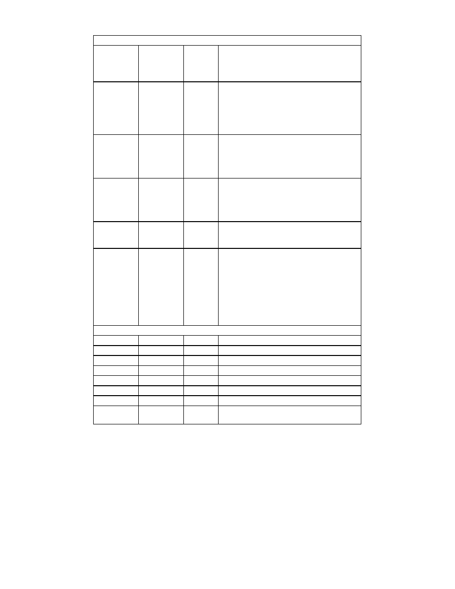
Table 1 - USB97C201 Buffer Type Descriptions
BUFFER
DESCRIPTION
I
Input
IS
Input with Schmitt trigger
IO8
Input/Output with 8 mA drive
O8
Output with 8mA drive
O12
Output with 12mA drive
IO20
Input/output with 20mA drive
OD12
Open drain....12mA sink
O20
Output with 20mA drive
ICLKx
XTAL clock input
OCLKx
XTAL clock output
I/O-U
Defined in USB specification
SMSC DS Ł USB97C201
Page 14
Rev. 08/08/2002
PRELIMINARY
6.0 FUNCTIONAL BLOCK DESCRIPTIONS
6.1 MCU
The 64K memory map is as follows from the 8051's viewpoint:
6.1.1
MCU MEMORY MAP: CODE SPACE
The 8051 has a single flat 64K Code space. External memory requires 80ns access times from Address to Data
and less than 80ns output enable access times, assuming the use of the nMEMR signal as OE on the memory.
Table 2 - MCU Code Memory Map
8051 ADDRESS
CODE SPACE
ACCESS
0x0700-0xFFFF
Fixed Memory
External Program
Memory
0x0400-0x06FF
768 Bytes of Fixed 16k FLASH Page
OR
768 Bytes of Internal SRAM for program execution
(see bit 7 of the UTIL_CFG register for more
information)
External Program
Memory
OR
Internal Program
SRAM
0x0000-0x03FF
Fixed Memory
External Program
Memory
8051 MCU External Code Address
Space
0xFFFF
Internal 768 Byte
SRAM or External
Memory
0x0000
64K
0x0400
0x0700
FIGURE 1 - MCU TO EXTERNAL CODE SPACE MAP

SMSC DS Ł USB97C201
Page 15
Rev. 08/08/2002
PRELIMINARY
6.1.2
MCU MEMORY MAP: XDATA SPACE
Table 3 - MCU XData Memory Map
8051 ADDRESS
DATA SPACE
ACCESS
0x3F30-0xFFFF
External Memory or I/O Devices
External
(IOR or IOW active)
0x3F00-0x3F2F
Internal Test Registers (reserved access)
DO NOT ACCESS
0x33F7-0X3EFF
External Memory or I/O Devices
External
(IOR or IOW active)
033F6
External ATA Interface I/O
External
(IOR or IOW active)
0x31F8-0x33F5
External Memory or I/O Devices
External
(IOR or IOW active)
0x31F0-0x31F7
External ATA Interface I/O
External
(IOR or IOW active)
0x30F4-0x31EF
External Memory or I/O Devices
External
(IOR or IOW active)
0X30F0-0X30F3
Internal Test Registers (reserved access)
DO NOT ACCESS
0X0700-0X30EF
External Memory or I/O Devices
External
(IOR or IOW active)
0x0400-0x06FF
768 Byte SRAM
Internal
0x0000-0x03FF
(see Note 1)
External
(IOR or IOW
active)(see Note 1)
Note 1: This XDATA space is accessed using MOVX instructions. A region of 8051 Special Function Registers
(SFR) is also accessible at 0x0100 to 0x01FF addresses using the MOV instructions. In addition to the
normal 8051 SFRs, there are also numerous Runtime Registers in this SFR space. These Runtime
Registers are external to the 8051, but internal to the USB97C201.

SMSC DS Ł USB97C201
Page 16
Rev. 08/08/2002
PRELIMINARY
6.1.3
MCU BLOCK REGISTER SUMMARY
Table 4 - MCU Block Register Summary
(These registers are external to the 8051 design core)
ADDRESS
NAME
R/W
DESCRIPTION
PAGE
RUNTIME REGISTERS
80
ISR_0
R/W
INT0 Source Register
20
93
IMR_0
R/W
INT0 Mask Register
21
90
ISR_1
R/W
INT1 Source Register
21
94
IMR_1
R/W
INT1 Mask Register
22
95
DEV_REV
R
Device Revision Register
22
96
DEV_ID
R
Device ID Register
22
UTILITY REGISTERS
97
GPIO_DIR
R/W
GPIO Direction Register
23
9A
GPIO_OUT
R/W
GPIO Data Output Register
25
9B
GPIO_IN
R
GPIO Data Input Register
25
C0
GPIO_IRQ
R/W
GPIO Interrupt Status Register (INT4)
25
9C
GPIO_MSK
R/W
GPIO Interrupt Mask Register (INT4)
26
9D
UTIL_CONFIG
R/W
Miscellaneous Configuration Register
27
9F
SRAM_DATA
R/W
SRAM Data Port Register
27
A1
SRAM_ADD1
R/W
SRAM Address 1 Register
28
A2
SRAM_ADD2
R/W
SRAM Address 2 Register
28
POWER MANAGEMENT REGISTERS
A5
CLOCK_SEL
R/W
8051 Clock Select Register
28
A0
WU_SRC_1
R/W
Wakeup Source 1 Register (INT2)
29
A6
WU_MSK_1
R/W
Wakeup Mask 1 Register (INT2)
29

SMSC DS Ł USB97C201
Page 17
Rev. 08/08/2002
PRELIMINARY
SIE & BUFFER CONTROL REGISTERS
A9
USB_ADD
R/W
USB Address Register
30
AA
SIE_CONF
R/W
SIE Configuration Register
30
AB
USB_STAT
R/W
USB Bus Status Register
31
AC
USB_MSK
R/W
USB Bus Status Mask Register
31
B0
SIE_STAT
R
SIE Status Register
32
AD
USB_CONF
R/W
USB Configuration Number Register
33
AE
SIE_MSK
R/W
SIE Status Mask Register
32
AF
EP0RX_CTL
R/W
Endpoint 0 Receive Control Register
33
B1
EP0TX_CTL
R/W
Endpoint 0 Transmit Control Register
33
B2
EP1RX_CTL
R/W
Endpoint 1 Receive Control Register
33
B3
EP1TX_CTL
R/W
Endpoint 1 Transmit Control Register
34
B4
EP2_CTL
R/W
Endpoint 2 Control Register
34
B5
EP0RX_BC
R/W
Endpoint 0 Receive Byte Count Register
36
B6
EP0TX_BC
R/W
Endpoint 0 Transmit Byte Count Register
36
B7
EP1RX_BC
R/W
Endpoint 1 Receive Byte Count Register
36
C7
EP1TX_BC
R/W
Endpoint 1 Transmit Byte Count Register
36
CE
RAMWRBC_A1
R/W
RAM Buffer Write Byte Count Register A1
37
CF
RAMWRBC_A2
R/W
RAM Buffer Write Byte Count Register A2
37
D1
RAMWRBC_B1
R/W
RAM Buffer Write Byte Count Register B1
37
D2
RAMWRBC_B2
R/W
RAM Buffer Write Byte Count Register B2
37
D3
RAMRDBC_A1
R/W
RAM Buffer Read Byte Count Register A1
37
D4
RAMRDBC_A2
R/W
RAM Buffer Read Byte Count Register A2
37
D5
RAMRDBC_B1
R/W
RAM Buffer Read Byte Count Register B1
37
D6
RAMRDBC_B2
R/W
RAM Buffer Read Byte Count Register B2
38
D7
NAK
R/W
NAK Status Register
38
D9
NAK_MSK
R/W
NAK Mask Register
38
DA
USB_ERR
R
USB Error Register
41
ATA CONFIGURATION REGISTERS
DB
MSB_ATA
R/W
MSB ATA Data Register
39
DC
LSB_ATA
R/W
LSB ATA Data Register
39
DD
ATA_CTL
R/W
ATA Control Register
41
DE
ATA_DMA
R/W
ATA Ultra DMA Timing Register
42
DF
IDE_TIM
R/W
IDE Timing Register
42
E1
ATA_CNT0
R/W
ATA Transfer Count Register 0
40
E2
ATA_CNT1
R/W
ATA Transfer Count Register 1
40
E3
ATA_CNT2
R/W
ATA Transfer Count Register 2
40
E4
ATA_CNT3
R/W
ATA Transfer Count Register 3
40
E5
ATA_SRCA
R/W
ATA Slew Rate Control A Register
44
E6
ATA_SRCB
R/W
ATA Slew Rate Control B Register
44

SMSC DS Ł USB97C201
Page 18
Rev. 08/08/2002
PRELIMINARY
Table 5 - 8051 Core SFR Register Summary
These registers are part of the 8051 design core itself.
REGISTER
BIT7
BIT6
BIT5
BIT4
BIT3
BIT2
BIT1
BIT0
ADDRESS
SP
81h
DPL0
82h
DPH0
83h
DPL1
84h
DPH1
85h
DPS
0
0
0
0
0
0
0
SEL
86h
PCON
SMOD0
Ł
1
1
GF1
GF0
STOP IDLE 87h
TCON
TF1
TR1
TF0
TR0
IE1
IT1
IE0
IT0
88h
TMOD
GATE
C/T
M1
M0
GATE
C/T
M1
M0
89h
TL0
8Ah
TL1
8Bh
TH0
8Ch
TH1
8Dh
CKCON
T2M
T1M
T0M
MD2
MD1
MD0
8Eh
SPC_
FNC
0
0
0
0
0
0
0
WRS 8Fh
EXIF
IE5
IE4
IE3
IE2
1
0
0
0
91h
MPAGE
92h
SCON0
SM0_0
SM1_0
SM2_0 REN_0 TB8_0
RB8_0 TI_0
RI_0 98h
SBUF0
99h
IE
EA
ES1
ET2
ES0
ET1
EX1
ET0
EX0
A8h
IP
1
PS1
PT2
PS0
PT1
PX1
PT0
PX0
B8h
TL2
CCh
TH2
CDh
PSW
CY
AC
F0
RS1
RS0
OV
F1
P
D0h
EICON
SMOD1
1
EPFI
PFI
WDTI
0
0
0
D8h
ACC
E0h
EIE
1
1
1
EWDI
EX5
EX4
EX3
EX2
E8h
B
F0h
EIP
1
1
1
PWDI
PX5
PX4
PX3
PX2
F8h
Notes:
¦
Bit WRS of the SPC_FNC register controls the operation of MOVX writes the program or XDATA bus of the
8051. Setting it to 0 ( the reset state), will direct writes to the XDATA bus, either to internal or external
destinations, while setting it to 1 will allow writes to the program memory bus to occur, either internally( if the
768 SRAM is the target) or externally.
¦
Bits MD2:0 of the CKCON SFR register (8Eh) control the cycle timing for external accesses using the nIOR and
nIOW signals. This allows slow peripheral devices to be attached. The values and corresponding strobe
widths are shown below:
MD2
MD1
MD0
NIOR/NIOW STOBE
(CLKS)
NIOR/NIOW STROBE (AT
30MHZ)
0
0
0
2
66ns
0
0
1
4
133ns
0
1
0
8
267ns
0
1
1
12
400ns
1
0
0
16
533ns
1
0
1
20
667ns
1
1
0
24
800ns
1
1
1
28
933ns

SMSC DS Ł USB97C201
Page 19
Rev. 08/08/2002
PRELIMINARY
Note: the strobe width will vary with the actual clock divider used for the processor. For example if, 16 Mhz is used,
an MD[2:0] value of 111 will result in a 28 clock strobe or 1866ns.

SMSC DS Ł USB97C201
Page 20
Rev. 08/08/2002
PRELIMINARY
6.1.4
MCU REGISTER DESCRIPTIONS
6.1.4.1 MCU Runtime Registers
Table 6 - Interrupt 0 Source Register
ISR_0
(0x80 - RESET=0x0C)
INTERRUPT 0 SOURCE REGISTER
BIT
NAME
R/W
DESCRIPTION
7
USB_STAT
R
1= USB Bus System Event has occurred. Check USB_STAT
register for the specific event(s). This must be cleared by
clearing the USB_STAT register.
6
SETUP
R/W
1= A SETUP packet was received on Endpoint 0. The EP0RX
bit of ISR_1 will not be set. If another SETUP packet is
received on Endpoint 0 while this bit is high, the bit will go
low and then immediately high again, to signal the duplicate
SETUP. If all other bits in this register are clear and the INT0
of the 8051is configured for edge triggering, then another
interrupt will be generated within the 8051. The firmware
must clear this bit by writing a "1" to it to allow the Enpoint 0
buffer to receive subsequent data packets during the SETUP
transaction. Receipt of these packets will set EP0RX in
ISR_1.
5
Reserved
R
This bit always reads a "0".
4
ATA_IRQ
R/W
External interrupt input from the ATA-66 Interface.
1 = An ATA interrupt has occurred.
3
RAMRD_B
R/W
1 = The current transfer from the SRAM B Buffer has been
completed. See Sections 6.7 and 6.9 for more detail. This bit
is also cleared by writing a "1" to the RAMRD_TOGGLE bit of
the EP2_CTL register.
2
RAMRD_A
R/W
1 = The current transfer from the SRAM A Buffer has been
completed. See Sections 6.7 and 6.9 for more detail. . This
bit is also cleared by writing a "0" to the RAMRD_TOGGLE bit
of the EP2_CTL register.
1
RAMWR_B
R/W
1 = The current transfer to the SRAM B Buffer has been
completed. This bit may be cleared by the internal hardware
state machine while operating in "Auto Transfer" mode. See
Sections 6.7 and 6.9 for more detail.
0
RAMWR_A
R/W
1 = The current transfer to the SRAM A Buffer has been
completed. This bit may be cleared by the internal hardware
state machine while operating in "Auto Transfer" mode. See
Sections 6.7 and 6.9 for more detail.
The bits in this register (except bit 7) are set to their POR values by writing a `1' to the corresponding bit. If not
masked by the corresponding bit in the IMR0 mask register, a "1" on any of these bits will generate a "1" on the
8051 core's external INT0 input.

SMSC DS Ł USB97C201
Page 21
Rev. 08/08/2002
PRELIMINARY
Table 7 - Interrupt 0 Mask
IMR_0
(0x93- RESET=0xFF)
INTERRUPT 0 MASK REGISTER
BIT
NAME
R/W
DESCRIPTION
7
USB_STAT
R/W
USB Bus System Event interrupt mask
0 = Enable Interrupt
1 = Mask Interrupt
6
SETUP
R/W
SETUP interrupt mask
0 = Enable Interrupt
1 = Mask Interrupt
5
Reserved
R/W
Reserved.
4
ATA_IRQ
R/W
External ATA-66 interrupt input mask
0 = Enable Interrupt
1 = Mask Interrupt
3
RAMRD_B
R/W
SRAM Buffer B Output Interrupt Mask
0 = Enable Interrupt
1 = Mask Interrupt
2
RAMRD_A
R/W
SRAM Buffer A Output Interrupt Mask
0 = Enable Interrupt
1 = Mask Interrupt
1
RAMWR_B
R/W
SRAM Buffer B Input Interrupt Mask
0 = Enable Interrupt
1 = Mask Interrupt
0
RAMWR_A
R/W
SRAM Buffer A Input Interrupt Mask
0 = Enable Interrupt
1 = Mask Interrupt
Note1: The mask bits do not prevent the status in the ISR_0 register from being set, only from generating an
interrupt.
Table 8 - Interrupt 1 Source Register
ISR_1
(0x90- RESET=0x00)
INTERRUPT 1 SOURCE REGISTER
BIT
NAME
R/W
DESCRIPTION
7
ZLP_EP0
R/W
1= A ZLP has been received on EP0RX.
6
Reserved
R
This bit always reads a "0".
5
ATA_PIO
R
This bit reflects that state of the PIO_COMPLETE bit (bit 6) of
the ATA_CTL register. It cannot be written directly.
4
EP1RX
R/W
1 = A Packet was successfully received on Endpoint 1 and
stored in the Buffer SRAM. OUT tokens will be NAK'd until this
bit is cleared.
3
EP1TX
R/W
1 = A Packet was successfully transmitted on Endpoint 1
from the Buffer SRAM. IN tokens will be NAK'd until this bit is
cleared.
2
EP0RX
R/W
1 = A non-SETUP, non ZLP Packet (see ISR_0 SETUP bit)
was successfully received on Endpoint 0 and stored in the
Buffer SRAM. OUT tokens will be NAK'd until this bit is
cleared.
1
EP0TX
R/W
1 = A Packet was successfully transmitted on Endpoint 0
from the Buffer SRAM. IN tokens will be NAK'd until this bit is
cleared.
0
SUSPEND
R/W
Suspend Ł If 3ms of IDLE state are detected by the hardware,
then this bit will be set.

SMSC DS Ł USB97C201
Page 22
Rev. 08/08/2002
PRELIMINARY
Note 1: The bits (except for bit 5)in this register are cleared by writing a `1' to the corresponding bit. If not masked
by the corresponding bit in the IMR1 mask register, a "1" on any of these bits will generate a "1" on the 8051 core's
external INT1 input.
Table 9 - Interrupt 1 Mask
IMR_1
(0x94- RESET=0xFF)
INTERRUPT 1 MASK REGISTER
BIT
NAME
R/W
DESCRIPTION
7
ZLP_EP0
R/W
Zero Length Packet Interrupt Mask
0 = Enable Interrupt
1 = Mask Interrupt
6
Resereved
R/W
Reserved. This bit should never be written to a "0".
5
ATA_PIO
R/W
ATA PIO Complete Interrupt Mask
0 = Enable Interrupt
1 = Mask Interrupt
4
EP1RX
R/W
Endpoint 1 Received Packet Interrupt Mask
0 = Enable Interrupt
1 = Mask Interrupt
3
EP1TX
R/W
Endpoint 1 Transmitted Packet Interrupt Mask
0 = Enable Interrupt
1 = Mask Interrupt
2
EP0RX
R/W
Endpoint 0 Received Packet Interrupt Mask
0 = Enable Interrupt
1 = Mask Interrupt
1
EP0TX
R/W
Endpoint 0 Transmitted Packet Interrupt Mask
0 = Enable Interrupt
1 = Mask Interrupt
0
SUSPEND
R/W
SUSPEND Interrupt Mask
0 = Enable Interrupt
1 = Mask Interrupt
Note 1: The mask bits do not prevent the status in the ISR_1 register from being set, only from generating an
interrupt.
Table 10 - Device Revision Register
DEV_REV
(0x95- RESET=0xXX)
DEVICE REVISION REGISTER
BIT
R/W
DESCRIPTION
[7:0]
XXh
R
This register defines additional revision information
used internally by SMSC. The value is silicon revision
dependent.
Table 11 - Device Identification Register
DEV_ID
(0x96- RESET=0x12)
DEVICE IDENTIFICATION REGISTER
BIT
R/W
DESCRIPTION
[7:0]
12h
R
This register defines additional revision information
used internally by SMSC

SMSC DS Ł USB97C201
Page 23
Rev. 08/08/2002
PRELIMINARY
6.1.4.2 Utility Registers
Table 12 - GPIO Direction Register
GPIO_DIR
(0x97- RESET=0x00)
GPIO DIRECTION REGISTER
BIT
NAME
R/W
DESCRIPTION
7
GPIO7
R/W
GPIO7 Direction
0 = In
1 = Out
6
GPIO6
R/W
GPIO6 Direction
0 = In
1 = Out
5
GPIO5
R/W
GPIO5 Direction
0 = In
1 = Out
4
GPIO4/nWE
R/W
GPIO4 Direction
0 = In
1 = Out
3
GPIO3/T1
R/W
GPIO3 Direction
0 = In
1 = Out
2
GPIO2/T0
R/W
GPIO2 Direction
0 = In
1 = Out
1
GPIO1/TXD
R/W
GPIO1 Direction
0 = In
1 = Out
0
GPIO0/RXD
R/W
GPIO0 Direction
0 = In
1 = Out
SMSC DS Ł USB97C201
Page 24
Rev. 08/08/2002
PRELIMINARY
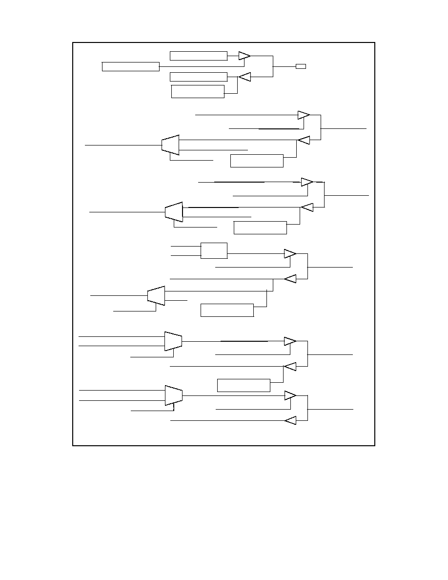
GPIO0
GPIO0 data out
RXD "Uart P3.0"
GPIO0 DIR
GPIO0 data in
0
1
S
"0"
GPIO1
0
1 S
GPIO1 data out
TXD "Uart P3.1"
GPIO1 DIR
GPIO1 data in
0
1
S
TBD
8051 "T1 timer P3.5"
GPIO3
GPIO3 data out
GPIO3 DIR
GPIO3 data in
0
1
S
Mux Enable
8051 "T0 timer P3.4"
TBD
GPIO2
GPIO2 data out
GPIO2 DIR
GPIO2 data in
GPIO[7:5]
GPIO Direction Bit
GPIO in data
GPIO out data
GPIO4/
nWE
0
1 S
GPIO4 data out
IDE_nIOW
GPIO4 DIR
GPIO4 data in
Edge Detector
Edge Detector
Edge Detector
Edge Detector
Edge Detector
Mux Enable
Mux Enable
Mux Enable
1 Hz
gate
Enable
Mux Enable
FIGURE 2 - GPIO MUXING BLOCK DIAGRAM

SMSC DS Ł USB97C201
Page 25
Rev. 08/08/2002
PRELIMINARY
Table 13 - GPIO Output Register
GPIO_OUT
(0x9A- RESET=0x00)
GPIO DATA OUTPUT REGISTER
BIT
NAME
R/W
DESCRIPTION
7
GPIO7
R/W
GPIO7 Output Buffer Data
6
GPIO6
R/W
GPIO6 Output Buffer Data
5
GPIO5
R/W
GPIO5 Output Buffer Data
4
GPIO4/nWE
R/W
GPIO4 Output Buffer Data
3
GPIO3/T1
R/W
GPIO3 Output Buffer Data
2
GPIO2/T0
R/W
GPIO2 Output Buffer Data
1
GPIO1/TXD
R/W
GPIO1 Output Buffer Data
0
GPIO0/RXD
R/W
GPIO0 Output Buffer Data
Table 14 - GPIO Input Register
GPIO_IN
(0x9B- RESET=0x00)
GPIO INPUT REGISTER
BIT
NAME
R/W
DESCRIPTION
7
GPIO7
R
GPIO7 Input Buffer Data
6
GPIO6
R
GPIO6 Input Buffer Data
5
GPIO5
R
GPIO5 Input Buffer Data
4
GPIO4/nWE
R
GPIO4 Input Buffer Data
3
GPIO3/T1
R
GPIO3 Input Buffer Data
2
GPIO2/T0
R
GPIO2 Input Buffer Data
1
GPIO1/TXD
R
GPIO1 Input Buffer Data
0
GPIO0/RXD
R
GPIO0 Input Buffer Data
Table 15 Ł GPIO Interrupt Status Register (INT4)
GPIO_IRQ
(0XC0- RESET=0x00)
GPIO INTERRUPT STATUS REGISTER
BIT
NAME
R/W
DESCRIPTION
7
GPIO7_IRQ
R/W
1 = A level change has occurred on GPIO7.
6
GPIO6_IRQ
R/W
1 = A level change has occurred on GPIO6.
5
GPIO5_IRQ
R/W
1 = A level change has occurred on GPIO5.
4
GPIO4_IRQ
R/W
1 = A level change has occurred on GPIO4.
3
GPIO3_IRQ
R/W
1 = A level change has occurred on GPIO3.
2
GPIO2_IRQ
R/W
1 = A level change has occurred on GPIO2.
1
GPIO1_IRQ
R/W
1 = A level change has occurred on GPIO1.
0
GPIO0_IRQ
R/W
1 = A level change has occurred on GPIO0.
Note 1: Writing a "1" (one) to a bit clears the bit and enables the detection of the next level transition. If not masked
by the corresponding bit in the GPIO_MSK register, "1" in any bit in this register will force a "1" on the 8051
core's external INT4 interrupt input.

SMSC DS Ł USB97C201
Page 26
Rev. 08/08/2002
PRELIMINARY
Table 16 Ł GPIO Interrupt Mask Register
GPIO_MSK
(0x9C- RESET=0xFF)
GPIO INTERRUPT MASK REGISTER
BIT
NAME
R/W
DESCRIPTION
7
GPIO7_MSK
R/W
1 = Prevents a high in the corresponding bit
in the GPIO_IRQ register from generating an
interrupt on the INT4 input to the 8051.
6
GPIO6_MSK
R/W
1 = Prevents a high in the corresponding bit
in the GPIO_IRQ register from generating an
interrupt on the INT4 input to the 8051..
5
GPIO5_MSK
R/W
1 = Prevents a high in the corresponding bit
in the GPIO_IRQ register from generating an
interrupt on the INT4 input to the 8051...
4
GPIO4_MSK
R/W
1 = Prevents a high in the corresponding bit
in the GPIO_IRQ register from generating an
interrupt on the INT4 input to the 8051...
3
GPIO3_MSK
R/W
1 = Prevents a high in the corresponding bit
in the GPIO_IRQ register from generating an
interrupt on the INT4 input to the 8051...
2
GPIO2_MSK
R/W
1 = Prevents a high in the corresponding bit
in the GPIO_IRQ register from generating an
interrupt on the INT4 input to the 8051...
1
GPIO1_MSK
R/W
1 = Prevents a high in the corresponding bit
in the GPIO_IRQ register from generating an
interrupt on the INT4 input to the 8051...
0
GPIO0_MSK
R/W
1 = Prevents a high in the corresponding bit
in the GPIO_IRQ register from generating an
interrupt on the INT4 input to the 8051...

SMSC DS Ł USB97C201
Page 27
Rev. 08/08/2002
PRELIMINARY
Table 17 - Utility Configuration Register
UTIL_CONFIG
(9D RESET=0x00)
UTILITY CONFIGURATION REGISTER
BIT
NAME
R/W
DESCRIPTION
7
SRAMSW
R/W
1 = The 768 byte SRAM is located at 0x0400-
0x06FF in the Code Space, instead of
external Memory.
0 = The 768 byte SRAM is located at 0x0400-
0x06FF in the XDATA space.
6
Reserved
R/W
Reserved. This bit should never be written to
a "1".
5
GPIO0_TOG
R/W
1 = GPIO0 Output Auto Toggle enabled.
0 = Disabled, normal operation occurs.
4
GPIO4/nWE
R/W
GPIO4/SOF Output Select Mux
0 = GPIO4
1 = The IDE_nIOW signal is output.
3
GPIO3/T1
R/W
P3.5 Timer 1 input trigger source
0 = GPIO3
1 = TBD
2
GPIO2/T0
R/W
P3.4 Timer 0 input trigger source
0 = GPIO2
1 = TBD
1
GPIO1/TXD
R/W
GPIO1/TXD Output Select Mux
0 = GPIO1
1 = P3.1
0
GPIO0/RXD
R/W
P3.0 RXD/GPIO0 Input Select Mux
0 = RXD<=GPIO0
1 = RXD<='0'
Note 1: GPIO0, when used as an output, will automatically toggle with 1second period and 50% duty cycle if
GPIO0_TOG is high.
Table 18 Ł SRAM Data Port Register
SRAM_DATA
(0x9F- RESET=0x00)
SRAM DATA PORT REGISTER
BIT
NAME
R/W
DESCRIPTION
[7:0]
SRAM_DATA
[7:0]
R/W
Data to be read or written
from/to the buffer SRAM. The
address of the data is
determined by the
SRAM_ADD1/2 registers. Data
to be written will be done so
upon write of this register.
While reads of the register
always reflects the data at the
memory location.
Note: a delay equal to at least
one NOP must exist between
setting the address in the
SRAM_ADDx registers and
reading or writing this register.
No delay is required in auto-
increment operation.

SMSC DS Ł USB97C201
Page 28
Rev. 08/08/2002
PRELIMINARY
Table 19 Ł SRAM Address Register 1
SRAM_ADD1
(A1 RESET=0x00)
SRAM ADDRESS REGISTER 1
BIT
NAME
R/W
DESCRIPTION
[7:0]
SRAM_ADD
[7:0]
R/W
This register contains lower
bits of the address in the buffer
RAM that the SRAM_DATA
register reads or writes.
Table 20 Ł SRAM Address Register 2
SRAM_ADD2
(0XA2- RESET=0x00)
SRAM ADDRESS REGISTER 2
BIT
NAME
R/W
DESCRIPTION
[7:3]
Reserved
R
These bits always read "0".
[2:0]
SRAM_ADD
[10:8]
R/W
This register contains upper
bits of the address in the buffer
RAM that the SRAM_DATA
register reads or writes.
Note: These registers will auto increment upon each read or write to the SRAM_DATA register.
6.1.4.3 MCU Power Management Registers
Table 21 - MCU Clock Source Select
CLOCK_SEL
(0XA5 - RESET=0x40)
MCU CLOCK SOURCE SELECT
BIT
NAME
R/W
DESCRIPTION
7
SLEEP
R/W
When PCON. 0 = 1 and SLEEP has been set to 1, the
ring oscillator will be gated off, then all oscillators will be
turned off for maximum power savings.
6
ROSC_EN
R/W
0 = Ring Oscillator Disable.
1 = Ring Oscillator Enable. ROSC_EN must be set to 1
before the MCU can be switched to the internal Ring
Oscillator Clock source.
5
MCUCLK_SRC
R/W
MCUCLK_SRC overrides MCUCLK_x clock select and
switches the MCU to the Ring Oscillator.
0 = Use Ring Oscillator. ROSC_EN must be enabled by
the MCU first.
1 = Use clock specified in MCU_CLK_[1:0]
[4:3]
MCU_CLK[1:0]
R/W
[4:3] = 00: 3.75MHz
[4:3] = 01: 7.5MHz
[4:3] = 10: 15MHz
[4:3] = 11: 30MHz
2
CLKVALID
R
Reflects the state of the PHY CLKVALID signal. When 1,
indicates that the internal clocks are stable and can be
used instead of the ring oscillator. After restarting the
clocks with the SUSPEND bit in the SIE_CONF register,
the code should wait 50us before polling this bit. This bit
is polled until it reads a "1" to see if the clocks are settled
before accessing any other non 8051 registers.
1:0]
Reserved
R
Always reads "0".
Note 1: The 8051 may program itself to run off of an internal Ring Oscillator having a frequency range between 8
and 24MHz. This is not a precise clock, but is meant to provide the 8051 with a clock source, without
running the 30MHz crystal oscillator or the PLL

SMSC DS Ł USB97C201
Page 29
Rev. 08/08/2002
PRELIMINARY
Note 2: Switching between fast and slow clocks is recommended to save power.
Note 3: Clock switching can be done on the fly as long as both clocks are running. When switching, it takes a
total of six clocks (3 clocks of the original clock plus 3 clocks of the switching clock) to guarantee the
switching.
Note 4: Time TBD is required from ROSC_EN=1 to MCUCLK_SRC=0.
Table 22 - Wakeup Source 1 Register (INT2)
WU_SRC_1
(0XA0 Ł RESET=0x00)
WAKEUP SOURCE 1
BIT
NAME
R/W
DESCRIPTION
[7:3]
Reserved
R/W
Reserved
2
USB_Rese
t
R/W
This bit is set when the SIE detects simultaneous logic lows on D+
and D- (Single-Ended 0) for 32 to 64 full speed bit times, or 4 to 8
low speed bit times (or 2.5<t<5.5us). The USB_Reset signal may
be as long as 10ms. SETUP tokens can be NAK'd for up to 10ms
after the Reset signal is released.
1
Resume
R/W
This bit is set on detection of Global Resume state (when there is a
transition from the "J" state while in Global Suspend).
0
EXT_INT
R
This bit will be set if the ATA_IRQ bit of the ISR_0 register is set OR
if the 8051 INT4 signal (GPIO Interrupts) is high.
Note 1: The bits 1 and 2 in this register are cleared by writing a `1' to the corresponding bit.
Note 2: Unmasked Wakeup Source bits restart the 8051 when its clock is stopped. This restarts the Ring
Oscillator and crystal oscillator for the MCU to resume from <500ĄA operation.
Note 3: To initiate USB Remote Wakeup, the SIE_Resume bit should be used in the SIE_CONF register.
Table 23 - Wakeup Mask 1 Register
WU_MSK_1 (Note 1)
(0XA6 - RESET=0xFF)
WAKEUP MASK 1
BIT
NAME
R/W
DESCRIPTION
[7:3]
Reserved
R
This bit always reads "1".
2
USB_Reset
R/W
External wakeup event.
0 = Enabled
1 = Masked
1
Resume
R/W
External wakeup event.
0 = Enabled
1 = Masked
0
EXT_INT
R/W
External wakeup event.
0 = Enabled
1 = Masked
Note 1: Interrupt events enabled by these bits are Ored and routed to the INT2 external interrupt input of the 8051
core.

SMSC DS Ł USB97C201
Page 30
Rev. 08/08/2002
PRELIMINARY
6.1.4.4 SIE & Buffer Control Registers
Table 24 ŁUSB Address Register
USB_ADD
(0xA9 Ł RESET=0x00)
USB ADDRESS REGISTER
BIT
NAME
R/W
DESCRIPTION
7
Reserved
R
This bit always reads a "1".
[6:0]
ADDR[6:0]
R
This is the USB bus address that the device will respond to
when the EN bit is set. These bits are cleared for a
USB_RESET condition. This is automatically set during
enumeration by the SIE.
Table 25 Ł SIE Configuration Register
SIE_CONF
(0xAA - RESET=0x40)
SIE CONFIGURATION REGISTER
BIT
NAME
R/W
DESCRIPTION
7
Reserved
R
This bit always reads a "0".
6
DISCONNECT
R/W
1 = Forces the PHY to the DISCONNECT state, removing the
RTERM resistor from the USB+ pin and forcing the PHY to ignore
signaling on the USB bus.
0= Normal operation.
[5:4]
Reserved
R
These bits always read "0".
3
Reserved
R/W
This bit is reserved. It must never be written to a "1".
2
SPEED
R
1 = High speed operation, if host is capable (See USB_STAT
register).
0 = Full Speed operation.
This bit is automatically set by the internal SIE during enumeration.
1
RESUME
R/W
1 = Forces the SIE to transmit Resume Signaling ("K" State) on the
line, if this capability has been enabled by the
SET_FEATURE_REMOTE_WAKEUP command form the host. This
bit is set by the 8051 after it wakes up from a power down state, for
remote wakeup operation. The USB97C201 appropriately times the
duration of this signaling in accordance with the USB specifications.
This bit will not be automatically cleared at the end of the RESUME
signaling.
Note: In order for the USB97C201 to generate a remote wake-up,
the SUSPEND bit in this register MUST be cleared (0).
0 = Normal operation
0
SUSPEND
R/W
1 = Forces the USB97C201's PHY into power down mode for
SUSPEND operation and to enable the detection of resume events
and the setting of the RESUME interrupts in USB_STAT and
WU_SRC_1 registers.
0 = This bit is cleared by the 8051 during wake-up operations
(RESUME or Remote RESUME) to re-power the PHY and enable its
clocks.
Note: In order for the USB97C201 to generate a remote wake-up
using bit 1 of this register, this bit MUST be cleared (0).
Note 1: If a SETUP packet is received on Endpoint 0 that is not automatically handled by the SIE (See Section
6.2.36.2.1) :
1.
Any STALL conditions will be cleared for EP0.
2.
An interrupt is generated, if unmasked, by the SETUP bit in the ISR_0 register.
SMSC DS Ł USB97C201
Page 31
Rev. 08/08/2002
PRELIMINARY
The reception of the packet will be indicated by the SETUP bits in the ISR_0 register being set. The pid
sequence is set to DATA-1 for both directions after a valid setup/DATA-0 transaction.
Table 26 - USB Bus Status Register
USB_STAT
(0xAB - RESET=0x00)
USB BUS STATUS REGISTER
BIT
NAME
R/W
DESCRIPTION
[7]
Reserved
R
This bit always reads "0".
6
EP2_ERR
R/W
1 = Indicates that a token in the opposite direction inferred
by the DIR bit of EP2_CTL register was received, ie an
unexpected IN or OUT token.
5
2.0
R/W
1 = Host is high speed capable. This bit is set if high
speed signaling is received from the host.
4
USB_RESUME
R/W
1 = Indicates that RESUME signaling has been detected.
This is only valid if the USB97C201 is in the SUSPEND
state via bit 0 of the SIE_CONF register.
3
USB_RESET
R/W
1 = Indicates that a USB Reset has been detected.
2
ERROR
R
1 = Indicates that a USB Error has been detected. See the
USB_ERR register for details. This bit is cleared by
clearing the USB_ERR register.
1
Reserved
R
This bit always reads "0".
0
Reserved
R
This bit always reads "0".
The bits in this register (except bit 2) are cleared by writing a `1' to the corresponding bit. These bits are ORed, if
unMASKED in the USB_MSK register, and drive a latch for the USB_STAT bit in the ISR_0 register.
Table 27 Ł USB Bus Status Mask Register
USB_MSK
(0xAC - RESET=0xFF)
USB BUS STATUS MASK REGISTER
BIT
NAME
R/W
DESCRIPTION
[7]
Reserved
R
This bit always reads "1".
6
EP2_ERR
R/W
1 = Prevents generation of the USB_STAT bit in the ISR_0
register when the EP2_ERR bit is set in the USB_STAT
register.
5
2.0
R/W
1 = Prevents generation of the USB_STAT bit in the ISR_0
register when the 2.0 bit is set in the USB_STAT register.
4
USB_RESUME
R/W
1 = Prevents generation of the USB_STAT bit in the ISR_0
register when the USB_RESUME bit is set in the
USB_STAT register.
3
USB_RESET
R/W
1 = Prevents generation of the USB_STAT bit in the ISR_0
register when the USB_RESET bit is set in the USB_STAT
register.
2
ERROR
R/W
1 = Prevents generation of the USB_STAT bit in the ISR_0
register when the ERROR bit is set in the USB_STAT
register.
1
Reserved
R
This bit always reads "1".
0
Reserved
R
This bit always reads "1".
Note1: The mask bits do not prevent the status in the USB_STAT register from being set, only from setting the
USB_STAT bit in the ISR_0 register.
SMSC DS Ł USB97C201
Page 32
Rev. 08/08/2002
PRELIMINARY
Table 28 Ł SIE Status Register
SIE_STAT
(0xB0 - RESET=0x00)
SIE STATUS REGISTER
BIT
NAME
R/W
DESCRIPTION
[7]
SET_STALL
R/W
Set to "1" if a SET_FEATURE_ENDPOINT_HALT command
is received on any endpoint by the SIE. Which endpoint is
STALLed can be determined by examining their CTL
registers.
6
CLR_STALL
R/W
Set to "1" if a CLEAR_FEATURE_ENDPOINT_HALT
command is received on any endpoint by the SIE. Which
endpoint's STALL condition is cleared can be determined
by examining their CTL registers.
5
SET_CONF
R/W
Set to "1" if a SET_CONFIGURATION command is received
on endpoint 0 by the SIE and the resulting configuration is
set and reported in the USB_CONFIG register.
4
Reserved
R
This read only bit always returns the value of "0".
3
SET_INTF
R/W
Set to "1" if a SET_INTERFACE command is received on
endpoint 0 by the SIE.
2
Reserved
R-
This read only bit always returns the value of "0".
1
SET_REMWU
R/W
Set to "1" if a SET_FEATURE_REMOTE_WAKE_UP
command is received on endpoint 0 by the SIE.
0
CLR_REMWU
R/W
Set to "1" if a
CLEAR_FEATURE_ENDPOINT_REMOTE_WAKE_UP
command is received on endpoint 0 by the SIE.
Note: These bits are masked by the SIE_MSK register and OR'd to drive the INT3 interrupt line into the 8051 core.
They may be cleared writing a "1" to the bit location.
Table 29 Ł SIE Status Mask Register
SIE_MSK
(0xAE - RESET=0xFF)
SIE STATUS MASK REGISTER
BIT
NAME
R/W
DESCRIPTION
[7]
SET_STALL
R/W
1= Disable interrupt generation.
0= Enable interrupt generation.
6
CLR_STALL
R/W
1= Disable interrupt generation.
0= Enable interrupt generation.
5
SET_CONF
R/W
1= Disable interrupt generation.
0= Enable interrupt generation.
4
Reserved
R
This read only bit always returns the value of "1".
3
SET_INTF
R/W
1= Disable interrupt generation.
0= Enable interrupt generation.
2
Reserved
R
This read only bit always returns the value of "1".
1
SET_REMWU
R/W
1= Disable interrupt generation.
0= Enable interrupt generation.
0
CLR_REMWU
R/W
1= Disable interrupt generation.
0= Enable interrupt generation.
Note: The mask bits do not prevent the status in the SIE_STAT register from being set, only from driving the INT3
line of the 8051 core high.

SMSC DS Ł USB97C201
Page 33
Rev. 08/08/2002
PRELIMINARY
Table 30 Ł USB Configuration Number Register
USB_CONF
(0xAD - RESET=0x00)
USB CONFIGURATION NUMBER REGISTER
BIT
NAME
R/W
DESCRIPTION
[7:4]
Reserved
R
Always returns a "0".
{3:0}
CONFIG
R
Reflects the current configuration number of the
USB97C201 system as set by the host.
Table 31 Ł Endpoint 0 Receive Control Register
EP0RX_CTL
(0xAF - RESET=0x00)
ENDPOINT 0 RECEIVE CONTROL REGISTER
BIT
NAME
R/W
DESCRIPTION
[7:4]
Reserved
R
This bit always reads "0".
3
DTOG
R
This bit reflects the data toggle state of the last received
data token.
2
STALL
R/W
When set to a "1", EP0 will respond with the STALL
handshake to OUT tokens EXCEPT a SETUP, which it will
ACK unconditionally. Either the internal SIE or the user may
set this bit. Receipt of a SETUP packet or USB RESET
clears this bit. Writing a "0" to this bit has no effect.
1
Reserved
R
This bit always reads "0".
0
ENABLE
R
Reads 1 if EP0 Receive is enabled by SIE.
Table 32 Ł Endpoint 0 Transmit Control Register
EP0TX_CTL
(0xB1 - RESET=0x00)
ENDPOINT 0 TRANSMIT CONTROL REGISTER
BIT
NAME
R/W
DESCRIPTION
7
Reserved
R
This bit always reads "0".
6
Reserved
R
This bit always reads "0".
5
Reserved
R
This bit always reads "0".
4
TX
R/W
When written with a "1", allows the SIE to transfer data from
the buffer SRAM to EP0. OUT tokens will be NAK'd until the
transfer has been completed. It is cleared by the SIE when
transmission of the packet has been completed.
3
Reserved
R
This bit always reads "0".
2
STALL
R/W
When set to a "1", EP0 TX will respond with the STALL
handshake to IN tokens. . Either the internal SIE or the user
may set this bit. Receipt of a SETUP packet or USB RESET
clears this bit. Writing a "0" to this bit has no effect.
1
Reserved
R
This bit always reads "0".
0
ENABLE
R
Reads "1" if EP0 Transmit is enabled by the SIE.
Table 33 Ł Endpoint 1 Receive Control Register
EP1RX_CTL
(0xB2 - RESET=0x00)
ENDPOINT 1 RECEIVE CONTROL REGISTER
BIT
NAME
R/W
DESCRIPTION
[7:4]
Reserved
R
This bit always reads "0".
3
DTOG
R
This bit reflects the data toggle state of the last received
data token.
2
STALL
R/W
When set to a "1", EP1 RX will respond with the STALL

SMSC DS Ł USB97C201
Page 34
Rev. 08/08/2002
PRELIMINARY
EP1RX_CTL
(0xB2 - RESET=0x00)
ENDPOINT 1 RECEIVE CONTROL REGISTER
BIT
NAME
R/W
DESCRIPTION
handshake to OUT tokens. . Either the internal SIE or the
user may set this bit. Receipt of a "CLEAR FEATURE
ENDPOINT CLEAR" command for this endpoint or USB
RESET clears this bit. Writing a "0" to this bit has no effect.
1
Reserved
R
This bit always reads "0".
0
ENABLE
R/W
EP1 Receive is enabled in the SIE if this bit is set to a "1",
otherwise, it is disabled.
Table 34 Ł Endpoint 1 Transmit Control Register
EP1TX_CTL
(0xB3 - RESET=0x00)
ENDPOINT 1 TRANSMIT CONTROL REGISTER
BIT
NAME
R/W
DESCRIPTION
7
Reserved
R
This bit always reads "0".
6
Reserved
R
This bit always reads "0".
5
Reserved
R
This bit always reads "0".
4
TX
R/W
When written with a "1", allows the SIE to transfer data from
the buffer SRAM to EP1. Until the transmission or reception
is complete, OUT will be NAK'd. It is cleared by the SIE
when transmission of the packet has been completed.
3
Reserved
R
This bit always reads "0".
2
STALL
R/W
When set to a "1", EP1 TX will respond with the STALL
handshake to IN tokens. . Either the internal SIE or the user
may set this bit. Receipt of a "CLEAR FEATURE
ENDPOINT CLEAR" command for this endpoint or USB
RESET clears this bit. Writing a "0" to this bit has no effect.
1
Reserved
R
This bit always reads "0".
0
ENABLE
R
EP1 Transmit is enabled in the SIE if this bit is set to a "1",
otherwise, it is disabled.
Table 35 Ł Endpoint 2 Control Register
EP2_CTL
(0xB4 - RESET=0x00)
ENDPOINT 2 CONTROL REGISTER
BIT
NAME
R/W
DESCRIPTION
7
DIR
R/W
Setting this bit to a "1" indicates that the data flow is from
the ATA interface to the SIE, a "0" indicates the opposite
direction. When a "1", the SIE will set the EP2_ERR bit in
the USB_STATUS register if an OUT token is received.
When a "0", the EP2_ERR bit set if the SIE receives an IN
token.
6
RAMWR_
TOGVALID
R/W
If this bit is set to a "1" when writes to this register occur,
then the value of bit 5 written to this register will have effect.
If cleared, then the values of bit 5, when this register is
written, is ignored. This bit always returns "0" on reads.
5
RAMWR_
TOGGLE
R/W
Writing a "0" to this bit will enable writing of the 512 byte
SRAM A buffer and clear the RAMWRBC_A1/2 registers,
while writing a "1" will select loading of the SRAM B buffer
and clear the RAMWRBC_B1/2 registers. This bit indicates
which interleaved buffer is currently or was last written with
data. The RAMWRBC_A and RAMWRBC_B Registers
contain the byte counts for the last write to the A and B input
buffers, respectively. See Sections 6.4, 6.5, and 6.9 for

SMSC DS Ł USB97C201
Page 35
Rev. 08/08/2002
PRELIMINARY
EP2_CTL
(0xB4 - RESET=0x00)
ENDPOINT 2 CONTROL REGISTER
BIT
NAME
R/W
DESCRIPTION
more information. To avoid interrupting a transfer that is in
progress, it is important not to write this bit until it is
completed. Note that if AutoToggle mode is enabled by bit
3 of the ATA_CTL register, this bit will reflect that current
buffer being written(1=B, 0=A).
W
Writing a "0" to this bit will begin the output of the 512 byte
SRAM A buffer to either the SIE or the ATA interface,
depending on the value of the DIR bit in this register, while
writing a "1" will begin outputting of SRAM B buffer. See
Sections 6.4, 6.5, and 6.9 for more information. The
RAMRDBC_A and RAMRDBC_B Registers determine how
many bytes will be output from either the A or B SRAM
buffer, respectively. Writing this bit to a "1" will clear the
RAMRD_B bit in the ISR_0 register, while writing it to "0"
will clear the RAMRD_A bit in that register.
Note: a delay of at least one NOP must exist before reading
the RAMRD_A or RAMRD_B bits in ISR0 when writing this
bit.
4
RAMRD_
TOGGLE
R
Upon reads, this bit will reflect the current or last buffer
being read (1=B, 0=A).
3
STALL_
RX
R/W
When set to a "1", EP2 RX will respond with the STALL
handshake to all tokens. . Either the internal SIE or the
user may set this bit. This bit is only cleared when a SET
FEATURE ENDPOINT 2RX CLEAR or SET
CONFIGURATION command is received on EP0 from the
host, or by a USB reset.
2
STALL_TX
R/W
When set to a "1", EP2 TX will respond with the STALL
handshake to all tokens. . Either the internal SIE or the
user may set this bit. This bit is only cleared when a SET
FEATURE ENDPOINT 2TX CLEAR or SET
CONFIGURATION command is received on EP0 from the
host, or by a USB reset.
1
RAMRD_
TOGVALID
R/W
This bit always reads "0". If this bit is set to a "1" when
writes to this register occur, then the value of bit 4 written to
this register will have effect. If cleared, then the values of bit
4, when this register is written, is ignored.
0
ENABLE
R
Reads "1" if EP2 is enabled by the SIE in either direction.
Notes:
¦
If the DIR bit is changed, then the RAMWR_TOGGLE bit must be written by the user to assure that the proper
buffer is selected. The user can NOT rely on reading the value of this bit to determine which buffer is active
immediately after changing the DIR bit.
¦
Bit 2, above, will set the STALL condition for both TX and RX directions of EP2. If the host clears the stall in
either direction, then both direction's STALL condition will be cleared. Bit 3 above will be reserved and always
read a "0".

SMSC DS Ł USB97C201
Page 36
Rev. 08/08/2002
PRELIMINARY
Table 36 Ł Endpoint 0 Receive Byte Count Register
EP0RX_BC
(0xB5 - RESET=0x00)
ENDPOINT 0 RECEIVE BYTE COUNT REGISTER
BIT
NAME
R/W
DESCRIPTION
7
Reserved
R
This bit always reads "0".
6
64BYTE
R
1 = Indicates that 64 Bytes were received.
[5:0]
COUNT
R
Indicates the byte count of the packet received on EP0 and
stored in SRAM beginning at address 0x0000.
Note: This register is updated at the end of a transfer and is actually the least significant bits of the ending address
in the SRAM buffer.
Table 37 Ł Endpoint 0 Transmit Byte Count Register
EP0TX_BC
(0xB6 - RESET=0x00)
ENDPOINT 0 TRANSMIT BYTE COUNT REGISTER
BIT
NAME
R/W
DESCRIPTION
7
Reserved
R
This bit always reads "0".
6
64BYTE
R/W
1 = Indicates that 64 Bytes are to be transmitted.
[5:0]
COUNT
R/W
Indicates the byte count of the packet to be sent on EP0
and stored in SRAM beginning at address 0x0040.
Note: A zero length packet may be sent by just clearing this register and setting the TX bit in the EP0TX_CTL
register.
Table 38 Ł Endpoint 1 Receive Byte Count Register
EP1RX_BC
(0xB7 - RESET=0x00)
ENDPOINT 1 RECEIVE BYTE COUNT REGISTER
BIT
NAME
R/W
DESCRIPTION
7
Reserved
R
This bit always reads "0".
6
64BYTE
R
1 = Indicates that 64 Bytes were received.
[5:0]
COUNT
R
Indicates the byte count of the packet received on EP1 and
stored in SRAM beginning at address 0x0080.
Notes:
¦
This register is updated at the end of a transfer and is actually the least significant bits of the ending address
in the SRAM buffer.
¦
This register is cleared if a SETUP packet is received on EP0.
Table 39 Ł Endpoint 1 Transmit Byte Count Register
EP1TX_BC
(0xC7 - RESET=0x00)
ENDPOINT 1 TRANSMIT BYTE COUNT REGISTER
BIT
NAME
R/W
DESCRIPTION
7
Reserved
R
This bit always reads "0".
6
64BYTE
R/W
1 = Indicates that 64 Bytes are to be transmitted.
[5:0]
COUNT
R/W
Indicates the byte count of the packet to be sent on EP1
and stored in SRAM beginning at address 0x00C0.
Note: A zero length packet may be sent by just clearing this register and setting the TX bit in the EP1TX_CTL
register.

SMSC DS Ł USB97C201
Page 37
Rev. 08/08/2002
PRELIMINARY
Table 40 Ł RAM Buffer Write Byte Count Register A1
RAMWRBC_A1
(0xCE - RESET=0x00)
RAM BUFFER WRITE BYTE COUNT REGISTER A1
BIT
NAME
R/W
DESCRIPTION
[7:2]
Reserved
R
This bit always reads "0".
1
512Bytes
R
1 = Indicates that 512 bytes were transferred
0
COUNT8
R
Bit 8 of the byte count for the data transferred.
Table 41 Ł RAM BUFFER WRITE Byte Count Register A2 Register
RAMWRBC_A2
(0xCF- RESET=0x00)
RAM BUFFER WRITE BYTE COUNT REGISTER A2
BIT
NAME
R/W
DESCRIPTION
[7:0]
COUNT[7:0]
R
Bits 7 thru 0 the byte count of the data transferred to the
SRAM. The data is stored beginning at address 0x0100
Table 42 Ł RAM Buffer Write Byte Count Register B1
RAMWRBC_B1
(0xD1 - RESET=0x00)
RAM BUFFER WRITE BYTE COUNT REGISTER B1
BIT
NAME
R/W
DESCRIPTION
[7:2]
Reserved
R
This bit always reads "0".
1
512Bytes
R
1 = Indicates that 512 bytes were transferred
0
COUNT8
R
Bit 8 of the byte count for the data transferred.
Table 43 Ł RAM Buffer Write Byte Count Register B2 Register
RAMWRBC_B2
(0xD2 - RESET=0x00)
RAM BUFFER WRITE BYTE COUNT REGISTER B2
BIT
NAME
R/W
DESCRIPTION
[7:0]
COUNT[7:0]
R
Bits 7 thru 0 the byte count of the data transferred to SRAM.
The packet is stored beginning at address 0x0300.
Table 44 Ł RAM Buffer Read Byte Count Register A1
RAMRDBC_A1
(0xD3 - RESET=0x00)
RAM BUFFER READ BYTE COUNT REGISTER A1
BIT
NAME
R/W
DESCRIPTION
[7:2]
Reserved
R
This bit always reads "0".
1
512Bytes
R/W
1 = Indicates that 512 bytes are to transferred
0
COUNT8
R/W
Bit 8 of the byte count for the data to be transferred.
Table 45 Ł RAM Buffer Read Byte Count Register A2 Register
RAMRDBC_A2
(0xD4 - RESET=0x00)
RAM BUFFER READ BYTE COUNT REGISTER A2
BIT
NAME
R/W
DESCRIPTION
[7:0]
COUNT[7:0]
R/W
Bits 7 thru 0 the byte count of the packet to be transferred
from the SRAM. The packet is stored beginning at address
0x0100
Table 46 Ł RAM Buffer Read Byte Count Register B1
RAMRDBC_B1
(0xD5 - RESET=0x00)
RAM BUFFER READ BYTE COUNT REGISTER B1
BIT
NAME
R/W
DESCRIPTION
[7:2]
Reserved
R
This bit always reads "0".
1
512Bytes
R/W
1 = Indicates that 512 bytes are to transferred
0
COUNT8
R/W
Bit 8 of the byte count for the data to be transferred.

SMSC DS Ł USB97C201
Page 38
Rev. 08/08/2002
PRELIMINARY
Table 47 Ł RAM Buffer Read Byte Count Register B2 Register
RAMRDBC_B2
(0xD6 - RESET=0x00)
RAM BUFFER READ BYTE COUNT REGISTER B2
BIT
NAME
R/W
DESCRIPTION
[7:0]
COUNT[7:0]
R/W
Bits 7 thru 0 the byte count of the packet to be transferred
from the SRAM. The packet is stored beginning at address
0x0300.
Table 48 Ł NAK Register (INT5)
NAK
(0xD7 - RESET=0x00)
NAK REGISTER
BIT
NAME
R/W
DESCRIPTION
7
NYET2RX
R
1 = indicates that an NYET has been sent to the host on
Endpoint 2 in response to an OUT token.
6
NYET0RX
R
1 = indicates that an NYET has been sent to the host on
Endpoint 0 in response to an OUT token.
5
NAK2TX
R
1 = indicates that an NAK has been sent to the host on
Endpoint 2 in response to an IN token.
4
NAK2RX
R
1 = indicates that an NAK has been sent to the host on
Endpoint 2 in response to an OUT token.
3
NAK1TX
R
1 = indicates that an NAK has been sent to the host on
Endpoint 1 in response to an IN token.
2
NAK1RX
R
1 = indicates that an NAK has been sent to the host on
Endpoint 1 in response to an OUT token.
1
NAK0TX
R
1 = indicates that an NAK has been sent to the host on
Endpoint 0 in response to an IN token.
0
NAK0RX
R
1 = indicates that an NAK has been sent to the host on
Endpoint 0 in response to an OUT token.
Notes:
¦
Any bit that is high in this register, if not masked by the corresponding mask bit in the NAK_MSK register will
generate INT5 to the 8051.
¦
A bit in this register may be cleared by writing a "1" to it.
Table 49 Ł NAK Mask Register
NAK_MSK
(0xD9- RESET=0xFF)
NAK MASK REGISTER
BIT
NAME
R/W
DESCRIPTION
7
NYET2RX
R/W
1 = Prevents generation of the 8051 INT5 interrupt when
the NYET2RX bit is set in the NAK register.
6
NYET0RX
R/w
1 = Prevents generation of the 8051 INT5 interrupt when
the NYET0RX bit is set in the NAK register.
5
NAK2TX
R/W
1 = Prevents generation of the 8051 INT5 interrupt when
the NAK2TX bit is set in the NAK register.
4
NAK2RX
R/W
1 = Prevents generation of the 8051 INT5 interrupt when
the NAK2RX bit is set in the NAK register.
3
NAK1TX
R/W
1 = Prevents generation of the 8051 INT5 interrupt when
the NAK1TX bit is set in the NAK register.
2
NAK1RX
R/W
1 = Prevents generation of the 8051 INT5 interrupt when
the NAK1RX bit is set in the NAK register.
1
NAK0TX
R/W
1 = Prevents generation of the 8051 INT5 interrupt when
the NAK0TX bit is set in the NAK register.
0
NAK0RX
R/W
1 = Prevents generation of the 8051 INT5 interrupt when

SMSC DS Ł USB97C201
Page 39
Rev. 08/08/2002
PRELIMINARY
NAK_MSK
(0xD9- RESET=0xFF)
NAK MASK REGISTER
BIT
NAME
R/W
DESCRIPTION
the NAK0RX bit is set in the NAK register.
Table 50 Ł USB Error Register
USB_ERR
(0xDA - RESET=0x00)
USB ERROR REGISTER
BIT
NAME
R/W
DESCRIPTION
7
Reserved
R
This bit always reads a "0".
6
TOKEN
R/W
When set, this bit indicates that an unexpected token has
been received on one of the device's endpoints.
5
Reserved
R
This bit always reads a "0".
4
STALL
R/W
When set, indicates that a token has been received on a
endpoint of the device while that endpoint is in the STALL
condition.
3
DTOG
R/W
When set, indicates that a data packet has been received
on one of the device's endpoints that has an incorrect data
toggle.
2
RXERR
R/W
When set, indicates that a packet has been received on
one of the device's endpoint with an error in FS mode.
1
Reserved
R
This bit always reads a "0".
0
CRC
R/W
When set, indicates that a packet with an incorrect CRC
has been received on an endpoint.
Note: Writing a "1" to a bit in this register will clear the bit.. If any bit is set in this register the USB_ERR bit is set in
the USB_STAT register.
Table 51 Ł MSB ATA Data Register
MSB_ATA
(0xDB - RESET=0x00)
MSB ATA CONTROL/STATUS DATA REGISTER
BIT
NAME
R/W
DESCRIPTION
[7:0]
D[15:8]
R/W
During 8051 writes to XDATA 0x31F0 (the ATA Drives
Control/Status register), data in this register represents the
MS byte of the 16 bit operation to this address. For a read
of 0x31F0, the MS byte data is returned in this register after
the PIO_COMPLETE bit is set in the ATA_CTL register. (the
data returned from the actual read of 31F0 should be
discarded)
Table 52 Ł LSB ATA Data Register
LSB_ATA
(0xDC - RESET=0x00)
LSB ATA CONTROL/STATUS DATA REGISTER
BIT
NAME
R/W
DESCRIPTION
[7:0]
D[7:0]
R/W
During 8051 reads to XDATA 0x31F1-7 and 33F6 (the ATA
Drive's 8 bit registers), the actual data is returned in this
register after the PIO_COMPLETE bit is set in the ATA_CTL
register. During writes, this register is unused.
For 8051 read to XDATA 0x31F0, the LS byte of data is
returned in this register after the PIO_COMPLETE bit is set
in the ATA_CTL register. During writes, this register is
unused.
SMSC DS Ł USB97C201
Page 40
Rev. 08/08/2002
PRELIMINARY
Table 53 Ł ATA Transfer Count Register 0
ATA_CNT0
(0xE1 - RESET=0x00)
ATA TRANSFER COUNT REGISTER 0
BIT
NAME
R/W
DESCRIPTION
[7:0]
D[7:0]
R/W
See note below.
Table 54 Ł ATA Transfer Count Register 1
ATA_CNT1
(0xE2 - RESET=0x00)
ATA TRANSFER COUNT REGISTER 1
BIT
NAME
R/W
DESCRIPTION
[7:0]
D[15:8]
R/W
See note below.
Table 55 Ł ATA Transfer Count Register 2
ATA_CNT2
(0xE3 - RESET=0x00)
ATA TRANSFER COUNT REGISTER 2
BIT
NAME
R/W
DESCRIPTION
[7:0]
D[23:16]
R/W
See note below.
Table 56 Ł ATA Transfer Count Register 3
ATA_CNT3
(0xE4 - RESET=0x00)
ATA TRANSFER COUNT REGISTER 3
BIT
NAME
R/W
DESCRIPTION
[7:0]
D[31:24]
R/W
See note below.
Note: The ATA_CNT[3:0] register must be written with the byte count of the total ATA transfer to be made. Writing the
ATA_CNT0 register initializes the ATA block for the transfer and should be written last. Reading these registers, will
return the actual number of bytes remaining to be transferred. If the transfer is prematurely terminated or aborted,
then the ATA_ERR bit in the ATA_CTL register will be set.

SMSC DS Ł USB97C201
Page 41
Rev. 08/08/2002
PRELIMINARY
Table 57 ŁATA Control Register
ATA_CTL
(0xDD - RESET=0x00)
ATA CONTROL REGISTER
BIT
NAME
R/W
DESCRIPTION
7
OUT_ CONTROL
R/W
Setting this bit to a "1" allows the IDE_SA[2:0], IDE_nIOR,
IDE_nIOW, IDE_nCS1, IDE_nCS0, IDE_DACK, and
IDE_D[15:0] pins operate normally. When cleared ("0"),
these pins are high impedance.
6
PIO COMPLETE
R/W
This bit is set once any PIO access to the external drive
registers (31F0-31F7 & 33F6) has been completed (see
Section 6.3.2 for more information on PIO accesses). This
bit is cleared by writing a "1" to it. The value of the this bit is
mirrored in the ISR_1 register to allow and interrupt to be
generated, if desired. This bit is also cleared at the start of
any PIO access to the external drive registers.
5
ATA_ABORT
R/W
Setting this bit to a "1" will abort any ATA transfer to/from the
external device. The ATA_ERR bit will be set, also. It is
cleared upon initializing the next ATA transfer by writing a
value into the ATA_CNT0 register.
4
ATA_ERR
R
A "1" on this bit indicates that an error has occurred during
the ATA transfer/to/from the drive. It is cleared upon
initializing the next ATA transfer by writing a value into the
ATA_CNT0 register.
3
AUTO_TOG
R/W
When set to "1", enables the automatic toggling between
the A and B SRAM buffers when writing to the SRAM. See
Section 6.9 on page 53 for more information
2
AUTO_TRANS
R/W
When set to a "1", enables the automatic transfer mode of
operation. See Section 6.9 on page 53 for details. Writing
this bit to a "1", automatically enables the automatic
toggling operation also, independent of the state of the
AUTO-TOG bit above.
1
Reserved
R
This bit always returns a "1".
0
EN0
R/W
Primary Drive 0 UDMA Enable.
1: Enable UDMA mode for primary channel drive 0.
0: Disable (default)..
Note: If an ATA_ERR occurs, the state of which buffers (A or B) are being used for reading or writing form/to the ATA
block are unchanged. The firmware may determine which buffer was being used by the ATA at the time of the error
by reading either bit 4 or bit 5 of the EP2_CTL register and determine how much of the transfer was completed by
reading the ATA_CNx registers.

SMSC DS Ł USB97C201
Page 42
Rev. 08/08/2002
PRELIMINARY
Table 58 ŁATA Ultra DMA Timing Register
ATA_DMA
(0xDE - RESET=0x00)
ATA ULTRA DMA TIMING REGISTER
BIT
NAME
R/W
DESCRIPTION
[7:3]
Reserved
R
These bits always reads "0".
[2:0]
DMA_TMG[2:0]
R/W
Drive Timing.
These bit settings the Ultra DMA mode that the ATA
interface operates when Ultra DMA operation is enabled.
They therefore determine the minimum data write strobe
Cycle Time (CT) and minimum Ready to Pause time (RP).
are shown below:
000: CT= 267ns, RP= 333ns (Mode 0)
001: CT= 167ns, RP= 266ns (Mode 1)
010: CT= 133ns, RP= 200ns (Mode 2)
011: CT= 100ns, RP= 200ns (Mode 3)
100: CT= 66ns, RP= 200ns (Mode 4)
101 thru 111 reserved
ULTRA DMA TIMING MODES
Mode (Data
Strobe
Cycle
Time)
Mode 0
(~1267ns)
Mode 1
(~167ns)
Mode 2
(~133ns)
Mode 3
(~100ns)
Mode 4
(~66ns)
Bit Settings
000
001
010
011
100
Table 59 Ł IDE Timing Register
IDE_TIM
(0xDF - RESET=0x00)
IDE TIMING REGISTER
BIT
NAME
R/W
DESCRIPTION
[7:6]
ISP[1:0]
R/W
IORDY Sample Point. This field selects the number of 30MHz
clocks (33ns/clock) between IDE_nIOx assertion and the first
IORDY sample point. In fast PIO timing mode (See bit 3
below), this sets the active period for the data strobe.
Bits [7-6]
Number of Clocks
00
5 clocks
01
4 clocks
10
3 clocks
11
2 clocks.
[5:4]
RT[0:1]
R/W
Recovery Time. This field selects the minimum number of
30MHz clocks(33ns/clock) between the last IORDY sample
point and the next IDE_nIOx strobe. In fast PIO timing mode
(See bit 3 below), this sets the inactive period for the data
strobe.
Bits [5-4]
Number of Clocks
00
4 clocks
01
3 clocks
10
2 clocks
11
1 clock.
3
DTE
R/W
DMA Timing Enable Only.
1: Fast timing mode is enabled for non-UDMA DMA data. PIO
transfer to the IDE data port will run in compatible timing.
0: Both non-UDMA DMA and PIO data transfers to drive will

SMSC DS Ł USB97C201
Page 43
Rev. 08/08/2002
PRELIMINARY
IDE_TIM
(0xDF - RESET=0x00)
IDE TIMING REGISTER
BIT
NAME
R/W
DESCRIPTION
use the fast timing mode.
2
PPE
R/W
Prefetch and Posting Enable.
1:Prefetch and posting to the IDE data port is enabled for the
drive.
0: Prefetch and posting is disabled for the drive .
1
ISPE
R/W
IORDY Sample Point Enable.
1: All accesses to the ATA I/O address range sample IORDY.
The IORDY sample point is specified by the "IORDY Sample
Point" field of this register.
0: IORDY sampling is disabled. The internal IORDY signal is
forced asserted guaranteeing that IORDY is sampled
asserted at the first sample point as specified by the "IORDY
Sample Point" field in this register.
0
FTB
R/W
Fast Timing Bank.
1: Accesses to the data port of the ATA IO address range
uses fast timings. PIO accesses to the data port use fast
timing only if bit 3 of this register is zero. Accesses to all non-
data ports of the ATA I/O address range always use the 8 bit
compatible timings.
0: Accesses to the data port of the ATA I/O address range
uses the 16 bit compatible timing.
Note: the following settings should be used for the ISP, RT, DTE, and FTB bits for the various PIO and MWDMA
modes:
MODE
ISP[1:0]
RT[1:0]
FTB
DTE
COMMENT
PIO Mode 0
00
11
1
0
ATA PIO cycle speed limited by 8051 data moves
PIO Mode 1
01
11
1
0
ATA PIO cycle speed limited by 8051 data moves
PIO Mode 2-4
10
11
1
0
ATA PIO cycle speed limited by 8051 data moves
MWDMA 0
00
00
0
x
requires compatibility mode timing to be used
MWDMA 1
10
10
1
x
MWDMA 2
10
11
1
x
SMSC DS Ł USB97C201
Page 44
Rev. 08/08/2002
PRELIMINARY
Table 60 ŁATA Slew Rate Control A Register
ATA_SRCA
(0xE5 - RESET=0x00)
ATA SLEW RATE CONTROL A REGISTER
BIT
NAME
R/W
DESCRIPTION
[7:6]
SLEW3
R/W
These two bits are control inputs of the ATA pad for data
bits [15:12]. The bits can be used to vary the slew rate of
IDE_D[15:12] from minimum to maximum rate specified by
the ATA66 specification. The value 11b sets the slew rate
to be the maximum and the value of 00b sets the slew rate
to be the minimum.
[5:4]
SLEW2
R/W
These two bits are control inputs of the ATA pad for data
bits [11:8]. The bits can be used to vary the slew rate of
IDE_D[11:8] from minimum to maximum rate specified by
the ATA66 specification. The value 11b sets the slew rate
to be the maximum and the value of 00b sets the slew rate
to be the minimum.
[3:2]
SLEW1
R/W
These two bits are control inputs of the ATA pad for data
bits [7:4]. The bits can be used to vary the slew rate of
IDE_D[7:4] from minimum to maximum rate specified by
the ATA66 specification. The value 11b sets the slew rate
to be the maximum and the value of 00b sets the slew rate
to be the minimum.
[1:0]
SLEW0
R/W
These two bits are control inputs of the ATA pad for data
bits [3:0]. The bits can be used to vary the slew rate of
IDE_D[3:0] from minimum to maximum rate specified by
the ATA66 specification. The value 11b sets the slew rate
to be the maximum and the value of 00b sets the slew rate
to be the minimum.
Table 61 ŁATA Slew Rate Control B Register
ATA_SRCB
(0xE6 - RESET=0x00)
ATA SLEW RATE CONTROL B REGISTER
BIT
NAME
R/W
DESCRIPTION
[7:2]
Reserved
R
Always returns "0" on reads
[1:0]
SLEW4
R/W
These two bits are control inputs of the ATA pad for
STROBE signaling during Ultra ATA writes to disk. The bits
can be used to vary the slew rate of STROBE from
minimum to maximum rate specified by the ATA66
specification. The value 11b sets the slew rate to be the
maximum and the value of 00b sets the slew rate to be the
minimum.
6.2 SIE Block
The SIE is a USB low-level protocol interpreter. The SIE controls the USB bus protocol, packet generation /
extraction, PID / Device ID parsing, and CRC coding / decodingwith autonomous error handling.
Parallel-to-serial / serial-to-parallel conversion, bit stuffing, and NRZI coding / decoding are handled in the PHY
block.
It is capable of operating either in USB 1.1 or 2.0 compliant modes. Unlike the normal 97Cxxx series SIEs, it has
more autonomous protocol handling functions like stall condition clearing on setup packets, suspend / resume /
reset conditions, and remote wakeup. It also autonomously handles the error conditions such as retry for CRC
errors, Data toggle errors, and generation of NYET, STALL, ACK and NACK depending on the endpoint buffer
status.

SMSC DS Ł USB97C201
Page 45
Rev. 08/08/2002
PRELIMINARY
During the power down state, the SIE clock is stopped. The SIE can asynchronously detect a USB Reset and/or
USB Resume condition and wakeup the 8051.
6.2.1
AUTONOMOUS USB PROTOCOL
6.2.1.1 Automatic Retries - Out Transactions
If a packet is received with an incorrect data toggle, the SIE will ACK, but ignores the data packet. If more than 64
bytes received on EP0RX or EP1RX, or if more than 512 bytes are received on EP2, the USB SIE will ignore the
packet and set the appropriate "STALL" bit until the host acknowledges the condition by sending a "CLEAR
FEATURE ENDPOINT STALL" command for that endpoint, or, in the case of Endpoint 0, a SETUP is recieved.
If an error occurs during an OUT transaction, the USB97C201 reloads its USB SIE read pointer back to the
beginning of the buffer. The host then sends another OUT token and retransmits the packet.
Once the packet has been successfully received, the appropriate interrupt bit is set in ISR_0 or ISR_1. The SIE can
handle any number of back-to-back retries, but the host determines how many times a packet is retried.
If an endpoints's buffer or buffers (in the case of EP2) are full, then the SIE sends a NACK. A TX direction Endpoint
will NAK all OUT packets.
6.2.1.2 Automatic Retries - In Transactions
If an timeout (No response from the host / lost ACK) occurs during an IN transaction, the USB97C201 reloads its
USB SIE side buffer read pointer back to the beginning of the failed packet. The host then sends another IN token
and the SIE re-transmits the packet with the same data toggle PID.
Once the host has successfully received the packet (only upon ACK received by SIE), the appropriate interrupt bit is
set in ISR_0 or ISR_1. The SIE can handle any number of back-to-back retries, but the host determines how many
times a packet is retried.
Upon reception of a SETUP token followed by the 8 byte DATA-0 packet on EP0, the internal DTOG bit for both
EP0RX and EP0TX are set to one.
6.2.1.3 Packet Lengths
The maximum packet length of an endpoint is fixed and 64 bytes for EP0 and EP1, and is 512 bytes for EP2 in HS
mode and 64 bytes in FS mode. For IN transactions, the USB97C201 will send the bytes in the buffer to the host.
For all OUT packets, the number of bytes received in the packet is indicated to the 8051 through the BYTE COUNT
Register of the respective endpoint.
6.2.2
USB EVENTS
There are several events, which cause different parts of the SIE to be initialized. The following is the list of events
and the respective actions.
6.2.2.1 Reset
A reset via the external nRESET pin causes the following:
1. All endpoints are disabled, all SIE endpoint buffers are cleared, all stall conditions, and all registers clear to
their default state.
2. If USB97C201 was in power down state, then it is cleared.
3. The external crystal oscillator is allowed to run.
6.2.2.2 USB Bus Reset
USB Bus Reset is recognized only when the clocks are running. If the device is in SUSPEND mode with the clocks
stopped, a USB RESET will be first recognized as a RESUME event and if the WU_SRC1 bit for RESUME is
unmasked, will restart the clocks. The USB RESET can only then be detected. Upon recognition it causes the
following:

SMSC DS Ł USB97C201
Page 46
Rev. 08/08/2002
PRELIMINARY
1. All SIE endpoint buffer byte count registers are cleared, all stall conditions, the SETUP bit, SETUP_DELAY bit,
SIE_SUSPEND, SIE_RESUME are cleared. The PID sequencers, internal DTOG are reset for all endpoints
2. The following registers will be set to their POR values: USB_ADD, SIE_STAT, USB_CONF, EP0RX_CTL,
EP0TX_CTL, EP1RX_CTL, EXP1TX_CTL, EP2_CTL, EP0RX_BC, EP0TX_BC, EP1RX_BC, EP1TX_BC,
RAMWRBC_A1, RAMWRBC_A2, RAMWRBC_B1, RAMWRBC_B2, RAMRDBC_A1, RAMRDBC_A2,
RAMRDBC_B1, RAMRDBC_B2, NAK, USB_ERR.
3. The seven bit USB device address is cleared.
4. Both EP0TX and EP0RX endpoints are enabled.
5. If the USB_RESET and USB_STAT bits are unmasked, then a ISR_0 interrupt (USB_STAT) is generated to the
8051 and the USB_RESET bit in the WU_SRC1 register will also be set and will generate an interrupt if
unmasked.
6.2.2.3 Suspend
This is detected by the SIE when the idle condition on the USB bus occurs for a duration of more than 3ms. Upon
detection of this condition via the SUSPEND bit of ISR_1, the 8051 will place the USB97C201 into a low power
mode via the USB_SUSPEND bit and enter into a power down state.
6.2.2.4 Setup token Arrival
When a SETUP token is recognized, the following sequence happens.
1. Independent of the state of SETUP bit, the setup data packet is received on EP0RX and ACK is sent for the
received setup packet.
2. The stall condition, if any, for EP0TX and EP0RX are cleared, as well as the EP0RX_BC and EP0TX_BC
registers and the TX bit of EP0_CTL register .
3. The internal DTOG bit for both EP0TX and EP0RX are set to one.
4. The EP0RX_BC register is cleared, allowing the subsequent data packet( if not zero length) to be written into
the start of the buffer.
5. The SETUP bit in ISR_0 register is set. Until the SETUP bit is cleared by the 8051, all OUT packets to EP0RX
are NACKed.
6.2.2.5 Resume
This global resume condition is recognized asynchronously and does not require the SIE clock running. Upon
recognition it causes the following. A USB RESET will be interpreted as a RESUME if it occurs while clocks are
stopped.
If the USB_RESUME and USB_STAT bits are unmasked, then a ISR_0 interrupt (USB_STAT) is generated to the
8051. Also the RESUME bit in the WU_SRC1 register will be set and can generate an interrupt, if unmasked.
The SIE_SUSPEND bit is cleared automatically and the SIE resumes from power down state.
6.2.2.6 Remote Wakeup
When the 8051 is required to go into power down state, the SIE_SUSPEND should be set. When a remote wakeup
event is desired, the 8051 is responsible to clear the SIE_SUSPEND, and set the SIE_RESUME bits.
6.2.3
STANDARD DEVICE REQUESTS
The SIE also handles autonomously several standard device requests received on Endpoint 0.
These requests are:
¦
SET_CONFIGURATION
¦
GET_CONFIGURATION
¦
SET_FEATURE_ENDPOINT_HALT
¦
CLEAR_FEATURE_ENDPOINT_HALT
¦
SET_FEATURE_REMOTE_WAKE_UP
¦
CLEAR_FEATURE_REMOTE_WAKE_UP
¦
GET_INTERFACE
¦
SET_INTERFACE
¦
SET_ADDRESS

SMSC DS Ł USB97C201
Page 47
Rev. 08/08/2002
PRELIMINARY
These events (except SET_ADDRESS, GET_INTERFACE (always returns 0), and GET_CONFIGURATION) are
indicated in the SIE_STATUS register, which can generate an interrupt to the 8051 core's INT3 line. The
configuration number, resulting from the SET_CONFIGURATION command is stored in the USB_CONF register.
This value is used when reporting to the host on a GET_CONFIGURATION Command, also. All other device
requests are handled normally and will generate the SETUP status bit when received.
6.2.4
SIE CONFIGURATIONS
Upon POR or the detection of USB RESET, the Configuration of the device is set to "0". The host may change its
Configuration state to "1" with a "SET CONFIGURATION" command on Endpoint 0. All other Configuration number
requests by the host will result in a STALL condition on Endpoint 0. For Configuration 0, only Endpoint 0 RX and TX
are enabled, while all endpoints are enabled for Configuration 1.
6.3 IDE Controller Description
This is an ATA-66 core. The PIO I/O address range for the ATA interface in the 8051 XDATA space is decoded in
the range of 0X31F0 to 0X31F7, and 0x33F6
Transfers to/from SRAM will occur from/to the 16 bit ATA Data Port at CS0=1, CS1=0, A2-A0= 0.
The most significant byte of transfer to/from this Data Port is available to the 8051 via the register located in SFR
space at 0xDB. Writes to 0x31F0 in the XDATA space by the 8051 would write both the contents of this register and
the data in the MOVEX instruction as a 16 bit DWORD to the ATA Data Port. Similarly, reads by the 8051 of 0x31F0
will return the actual drive data for reading by the 8051 at 0xDB and 0xDC.
6.3.1
IDE CONFIGURATIONS
The USB97C201 supports only a single primary drive on the IDE interface.
6.3.2
PIO IDE OPERATIONS
The IDE controller includes both compatible and fast timing modes. The fast timing mode only applies to the IDE
data ports. All other transactions to the IDE registers are run in single transaction mode with compatible timings.
The IDE_TIM register permits different timing modes, from Multi-word DMA ATA Mode 0 to ATA Mode 2, to be
programmed for the drive. These modes range from 3MB/sec to 16MB/sec in terms of data transfer rate. The Ultra
ATA/66 synchronous DMA timing modes can also be applied to each drive by programming the ATA_CTL and
ATA_DMA registers. When a drive is enabled in Ultra DMA mode operation, the DMA transfers are executed with the
Ultra ATA timings. The PIO data transfers are still executed using compatible timings or fast timings when
enabled.
PIO accesses are not directly made to the drive from the 8051 via its XDATA address space, but are timed by the
ATA controller to meet required drive timing. A read access is accomplished by first reading the XDATA address
location, ignoring the returned data, and then waiting for the PIO_COMPLETE bit to be set in the ATA_CTL register.
The actual data retrieved from the drive can then be read at LSB and MSB( if a 16 bit access to 31F0) ATA Data
registers in SFR space. Writes to the drive are done normally, directly to the XDATA address desired( the MSB ATA
Data register must be loaded first for the 16 bit writes to 31F0), but a subsequent write (or read) cannot be initiated
until the PIO_COMPLETE bit is set. This bit is reflected in the ISR_1 register to allow an interrupt to be generated, if
desired.
Startup Latency: If the IDE_SA[2:0] and IDE_nCS[1:0] lines are not set up, startup latency is incurred when a cycle
that accesses the IDE data port is decoded. Startup latency provides the setup time for assertion of IDE_SA[2:0]
and IDE_nCS[1:0] lines prior to assertion of the read and write strobes (IDE_nIOR and IDE_nIOW).
Cycle Latency: Cycle latency consists of the I/O command strobe assertion length and recovery time. Recovery
time is needed so that back-to-back transactions, which does not incur startup and shutdown latency, may occur
on the IDE interface without violating minimum cycle periods for the IDE interface. The command strobe assertion
width (IORDY Sample Point: ISP) for the fast timing mode is programmable in the ISP field of the IDE_TIM
Register. The recovery time (RCT) is programmable in the RCT field of the IDE_TIM Register.
If the IORDY is asserted when the IORDY sample point is reached, no wait states are added to the command
strobe assertion length. If IORDY is negated when the sample point is reached, additional wait states are added.
SMSC DS Ł USB97C201
Page 48
Rev. 08/08/2002
PRELIMINARY
IORDY Masking: The IORDY signal can be ignored and assumed asserted at the first IORDY Sample Point (ISP)
through the IDE_TIM register.
Shutdown Latency: Shutdown latency is incurred after the IDE data transactions (either a non-empty write post
buffer to the IDE drive or an outstanding read prefetch cycles from the IDE drive) have completed and before other
IDE transactions can proceed. The latency provides hold time on the IDE_SA[2:0] and IDE_nCS[1:0] lines with
respect to the read and write strobes (IDE_nIOR and IDE_nIOW). Shutdown latency is set to 67ns in duration.
Table 62 shows the IDE cycle timings for various IDE transaction types.
Table 62 Ł IDE Transaction Timing
IDE TRANSACTION TYPE
STARTUP
LATENCY
ISP
RCT
SHUTDOWN
LATENCY
Non-Data Port Compatible
133ns
367ns
733ns
67ns
Data Port Compatible
100ns
200ns
467ns
67ns
Fast Timing Mode (for Data
Port Accessing)
67ns
267-167ns
33-133ns
67ns
6.3.3
PIO IDE DATA PREFETCHING AND POSTING
The IDE Controller can be programmed via the IDE_TIM registers to allow data to be posted to and prefetched from
the IDE data ports. Data prefetching is initiated when a data port read occurs. The read prefetch eliminates latency
to the IDE data ports and allows them to be performed back to back for the highest possible PIO data transfer
rates. The first data port read of a sector is called the demand read. Subsequent data port reads from the sector
are called prefetch reads. The demand read and all prefetch reads must be of the same size (16 or 32 bits).
Data posting is performed for writes to the IDE data ports. The IDE CONTROLLER will then run the IDE cycle to
transfer the data to the drive.
6.3.4
DMA TRANSFERS
When enabled and supported by the device, DMA transfers are executed on the IDE interface, the chip selects
(IDE_nCS1/0) will be negated (high). When the IDE device asserts IDE_DRQ, the IDE Controller will return
IDE_nDACK to the IDE device when it is ready for the DMA data transfer. For multiword DMA transfers, the
IDE_nIOR or IDE_nIOW signal will free run at the programmed rate as long as IDE_DRQ remains asserted and
the IDE Controller is prepared to complete a data transfer. If IDE_DRQ has not de-asserted by the rising edge of
IDE_nIOR or IDE_nIOW signal multiword DMA is assumed and at least one more cycle will be executed. If
IDE_DRQ de-asserts before IDE_nIOR or IDE_nIOW is de-asserted while IDE_nDACK is asserted, it indicates
that one last data transfer remains for the current session. In this case, IDE_nDACK will be de-asserted one clock
after the IDE_nIOR or IDE_nIOW signal de-asserts. This allows the IDE controller to support both single and
multiword DMA cycles automatically.
The IDE device's DMA request signal is sampled when the IO strobe is deasserted. If inactive, the DMA
Acknowledge signal is deasserted and no more transfers take place until DMA request is again asserted.
The controller transfers data to or from the EP2 buffer(s) responding to the DMA requests from the IDE device. The
controller will continue this until stopped or the byte count in ATA_CNT[3:0] reaches zero.
6.3.4.1 Completion of DMA Data Transfers
The IDE device signals an interrupt (IDE_IRQ) once its programmed data count has been transferred or an error
occurs. The IDE device will also deassert its DMA request signal, causing the IDE Controller to stop transferring
data. On reads from the IDE device, it will cause any data read from the device to be transferred to the EP2
buffer(s), as they become available.

SMSC DS Ł USB97C201
Page 49
Rev. 08/08/2002
PRELIMINARY
6.3.5
ULTRA ATA/66 SYNCHRONOUS DMA OPERATION
Ultra ATA/66 is a new IDE transfer protocol used to transfer data between a Ultra ATA/66 capable IDE controller
and Ultra ATA/66 capable IDE devices. Ultra DMA/66 utilizes a "source synchronous" signaling protocol to transfer
data at rates up to 66 Mbytes/sec.
6.3.5.1 Ultra ATA/66 Signals
Although no additional signal pins are required for Ultra ATA/66 operation, the operation of some standard IDE
controller pins are redefined during Ultra ATA modes of operation. The Ultra DMA/66 protocol defines three hand-
shaking signals: STOP, STROBE and DMARDY. Table 63 shows the mapping of the redefined Ultra ATA/66
signals onto the standard IDE controller pins.
STOP: STOP is always driven by the the USB97C201 and is used to request that a transfer be stopped or as an
acknowledgment to stop a request from IDE device. The IDE_nIOW signal is redefined as STOP for both read and
write transfers.
STROBE: This is a data strobe signal driven by the TRANSMITTER of a data transfer, which is either the IDE device
of a DMA Read transfer or the USB97C201 of a DMA Write transfer, on which data is transferred during each rising
and falling edge transition of the signal. The IORDY signal is redefined as STROBE for reads (when transferring
data from the IDE device to the USB97C201). The IDE_nIOR signal is redefined as STROBE for writes (transferring
data from the USB97C201 to the IDE device).
nDMARDY: This is a signal driven by the RECEIVER of a data transfer, which is either the USB97C201 of a DMA
Read transfer or the IDE device of a DMA Write transfer, to signal that the RECEIVER is ready to transfer data or to
add wait states to the current transaction. The IDE_nIOR signal is redefined as nDMARDY for reads (when
transferring data from the IDE device to the USB97C201). The IORDY signal is redefined as nDMARDY for writes
(transferring data from the USB97C201 to the IDE device).
Table 63 Ł ULTRA ATA/66 Control Signal Assignments
STANDARD
IDE SIGNAL
NAME
SIGNAL NAME
DURING ULTRA
ATA/66 READ
CYCLE
SIGNAL NAME
DURING ULTRA
ATA/66 WRITE
CYCLE
IDE_nIOW
STOP
STOP
IDE_nIOR
nDMARDY
STROBE
IORDY
STROBE
nDMARDY
Note:
"Ultra ATA/66 Read Cycle": Data transfers are from the IDE device to the USB97C201.
"Ultra ATA/66 Write Cycle": Data transfers are from the USB97C201 to the IDE device.
6.3.6
ULTRA ATA/66 OPERATION
After initialization, there are two primary operations provided by the Ultra ATA/66 controller: data transfers and cyclic
redundancy checking (CRC).
6.3.6.1 Initialization
Initialization includes enabling and performing proper set up on the USB97C201and the IDE device. For the
USB97C201, it is necessary to enable Ultra ATA/66 mode for the IDE device and setting up the Ultra ATA/66 cycle
timings through the ATA_DMA register. The USB97C201 supports five timing modes: Mode 0 (120ns cycle time),
Mode 1 (80 ns cycle time), Mode 2 (60ns cycle time), Mode 3 (45ns cycle time), and Mode 4 (30ns cycle time).
6.3.6.2 Data Transfer Operation
The USB97C201 and the Ultra ATA compatible IDE device control the transfer via the Ultra ATA protocol. The actual
data transfer consists of three phases, a start-up phase, a data transfer phase, and a burst termination phase.

SMSC DS Ł USB97C201
Page 50
Rev. 08/08/2002
PRELIMINARY
1) Start-Up Phase: The IDE device begins the start-up phase by asserting DRQ signal. When ready to begin the
transfer, the USB97C201 will assert nDACK. When nDACK is asserted, the USB97C201 will drive CS0/1
inactive, and A0-A2 low.
¦
For Write cycles, the USB97C201 will deassert STOP, wait for the IDE device to assert nDMARDY and
then drive the first data word and the STROBE signal.
¦
For Read cycles, the USB97C201will tristate the data lines, deassert STOP, and assert nDMARDY. The
IDE device will then drive the first data word and the STROBE signal.
2) Data-Transfer Phase: The burst data transfer continues with the data source (Writes: USB97C201, Reads:
IDE devices) providing data and toggling STROBE. Data is transferred (latched by receiver) on each rising and
falling edge of STROBE.
¦
The source can pause the burst stream by holding STROBE high or low, resuming the burst stream by
again toggling STROBE.
¦
The receiver can pause the burst stream by negating the nDMARDY and resumes the transfers by
asserting nDMARDY.
The USB97C201 may pause a burst transaction in order to toggle internal data buffer, or to prevent a buffer over or
under flow condition, resuming once the condition has cleared.
1) Termination Phase: Either the source or the receiver can terminate a burst transfer. A burst termination
consists of a Stop Request, Stop Acknowledge and transfer of CRC data.
¦
The USB97C201 can stop a burst by asserting STOP, with the IDE device acknowledged by deasserting
DRQ.
¦
The IDE device stops a burst by deasserting DRQ and the USB97C201 acknowledges by asserting
STOP.
¦
The source then drives the STROBE signal to a high level. The USB97C201 then drive the CRC value
onto the data lines and deassert nDACK. The IDE devices will latch the CRC value on the rising edge of
nDACK.
The USB97C201 will terminate a burst transfer if a Programmed I/O (PIO) cycle is executed to the IDE channel
currently running the burst, or upon transferring the last data from the final PRD.
At the completion of the entire transfer process, the IDE device will issue an interrupt, setting the ATA_IRQ bit and
forcing the remaining data to be sent to host on read operations.
6.3.6.3 Cyclic Redundancy Checking (CRC) Calculation
Cyclic Redundancy Checking (CRC-16) is used for error checking on Ultra ATA/66 transfers. The CRC value is
calculated for all data by both the USB97C201 and the IDE device over the duration of the DMA burst transfer
segment. This segment is defined as all data transferred with a valid STROBE edge from DACK assertion to
nDACK deassertion. At the end of the transfer burst segment, the USB97C201 will drive the CRC value onto the
D[15:0] signals. The value is then latched by the IDE device on deassertion of nDACK. The IDE device compares
the USB97C201 CRC value to its own and reports an error if there is a mismatch.
6.4 SRAM Buffers
1.25K Bytes of Buffer SRAM are provided. The Memory Map of the buffers are given below:
Table 64 ŁBuffer SRAM Mapping
SRAM ADDRESS
BUFFER DESCRIPTION
0x300 Ł 0x4FF
SRAM B 512 byte EP2/ATA buffer
0x100 Ł 0x2FF
SRAM A 512 byte EP2/ATA buffer
0x0C0 Ł 0x0FF
64 Byte EP1 TX Buffer
0x080 Ł 0x0BF
64 Byte EP1 RX Buffer
0x040 Ł 0x07F
64 Byte EP0 TX Buffer
0x000 Ł 0x03F
64 Byte EP0 RX Buffer

SMSC DS Ł USB97C201
Page 51
Rev. 08/08/2002
PRELIMINARY
Note: The above SRAM address in the table refers to the BYTE location within the SRAM. The SRAM is actually
physically organized as a 32 bit wide memory.
The buffers used for EP2 is organized as two 512 byte buffers: A and B. The A buffer has its address starting at
0X100, while the B is at address 0X300.. Byte counts for data received or to be transmitted is contained in the
RAMWRBC_A/B and RAMRDBC_A/B register sets, respectively. The direction of data flow is determined by the DIR
bit in the EP2 Control register. If DIR=0 then data flow is from the SIE to SRAM and from the SRAM to the ATA
interface. If DIR=1 the data flow is in the opposite direction. Unlike EP0 and EP1, data for both directions can not be
simultaneously buffered in the SRAM for EP2. However, the dual buffers and automatic transfer operation (see
Section 6.9) allow for sustained 480Mbps transfers across the USB97C201.
6.5 8051 Options
The following 8051 core options are included:
¦
256 SRAM in SFR space
¦
Three timers
¦
Single serial port
¦
Extended external inputs (INT2-13)
¦
External program memory and external data bus (XDATA) are pinned out as a common bus.
6.6 Address Multiplexing
Access to the SRAM for the three access points, ie SIE, ATA DMA, or 8051, is via a time division multiplexing
scheme (See Section 6.7). Each of the above blocks have access to read or write the SRAM during one of four sub-
periods (the fourth period being reserved for future expansion/idle) of a four phase 15 Mhz clock( ie 60 Mhz slice
clock). The values set in the EPx_BUFx , and IN_BUFx, or OUT_BUFx (depending on the direction set for EP2)
control the address counter for accesses by the EPs during their time-slice.
The IN_BUFx or OUT_BUFx (again,depending on the direction of EP2) controls the address for ATA access and
SRAM_ADDx does so for the 8051 accesses.
Which endpoint has access during the SIE's time-slice is determined by the SIE, ie depending on what endpoint is
currently active on the USB bus. Since accesses occur at 15Mhz using DWORDs (32bits), this process is capable
of real time concurrency with the USB bus and does not require additional buffering in the SIE. Even if a received
packet is ultimately discarded, all that is required to do so is simply not generate the completion interrupt for that
endpoint. Similarly for the transmit process, allowing re-transmission.
6.7 SRAM Time Multiplexer Operation
The SRAM access, read or write, occurs in four sequential phases, ž0-3. These periods are 16.666ns long
(60Mhz) and are non-overlapping. Data to/from the SRAM are buffered by local DWORD latches close to the SRAM
to minimize high-speed bussing. The rest of the USB97C201 subsystems access these latches during the
phases when they are NOT being used to transfer data to/from the SRAM.
6.7.1
PHASE 0 (ž0)
During this phase, the SIE has access to the SRAM through its associated DWORD latches.
If data from EP0 or EP1 is ready (ie either a full DWORD or the end of a packet has been received), this data will be
written into the appropriate buffer address space and the associated EPxRX_BUF register incremented to reflect
the amount of buffer used to this point. If data to EP0 or EP1 is required by the SIE, it will load the data from the
SRAM into the DWORD latch whose address is determined by an incrementing address counter. This counter will
be compared against the EPx_TX register value, to determine if the buffer transfer has been completed.
If the DIR bit in EP2_CTL is "0", and data is requested by the SIE for transmission to the host on EP2, the TOKEN
error bit in the USB_ERR register will be set and no other action occurs. If data is received by the SIE on EP2 (IN
tokens) and either a full DWORD or EOP has been received, then this data will be written into either the SRAM A or
SRAM B buffer space, as appropriate, and the associated RAMWRBC_A/B registers incremented.

SMSC DS Ł USB97C201
Page 52
Rev. 08/08/2002
PRELIMINARY
If the DIR bit in EP2_CTL is "1", and data is received by the SIE from the host on EP2, the TOKEN error bit in the
USB_ERR register will be set and no other action occurs. If data to EP2 is required by the SIE from the SRAM, the
data will be loaded in the DWORD latch from the A or B buffer space, as appropriate. The SRAM data address will
be determined by an incrementing address counter which will be compared against the RAMRDBC_A/B registers'
value to determine if the buffer transfer has been completed.
6.7.2
PHASE 1 (ž1)
The ATA interface block has access to the SRAM via a DWORD latch during this phase.
I
f the DIR bit in EP2_CTL is "1", when either a full DWORD or end of DMA has been received by the ATA interface
from the ATAPI/ATA device and loaded in to the DWORD latch, it will be written into either the A or B buffer space, as
appropriate, and the associated RAMWRBC_A/B registers incremented.
If the DIR bit in EP2_CTL is "0", data will be loaded in the DWORD latch from the A or B buffer space, as
appropriate, when the ATA interface requires data to be sent to the ATAPI/ATA device. The SRAM data address will
be determined by an incrementing address counter, which will be compared against the RAMRDBC_A/B registers'
value to determine if the buffer transfer has been completed.
6.7.3
PHASE 2 (ž2)
During this phase, the DWORD latch that interfaces to the SRAM_DATA register will be normally repetitively loaded
with data READ from the SRAM at the address determined by the higher order bits of the SRAM_ADD1/2 register.
The 8051 can read this data with a read to the SRAM_DATA port. Bits 0&1 of the SRAM_ADD1 register will
determine the byte read of the DWORD latch.
In order to write data from the 8051 to the SRAM, the 8051 will write the data into the SRAM_DATA register. The
sub-byte of the DWORD latch determined by bits 0 & 1 of the SRAM_ADD1 register will be updated, and the entire
DWORD will be written to the SRAM at the address determined by the higher order address bits of the
SRAM_ADD1/2 registers during the next ž2 interval. Subsequently, it will return to reading the SRAM data into the
DWORD latch on each ž2 interval. This allows single byte modifications of the the 32 bit wide SRAM to be
executed by the 8051.
6.7.4
PHASE 3 (ž3)
Phase 3 is an idle period during which no accesses occur to the SRAM. This period is reserved for future
expansion in derivative products to allow another high speed access path for additional IO.
6.8 EP2 SRAM Buffer Operation
In order to illustrate the operation of the buffering and the interactions between the SIE and ATA control blocks and
the firmware, the following scenario will be explained in detail in a timeline format for operation NOT using the Auto
Toggle or Auto Transfer features (ie totally firmware controlled):
1. Endpoint 2 is currently receiving data (ie a file segment) from the host for transfer to the ATA interface (DIR bit
of EP2_CTL = 0). The SRAM B buffer assigned to EP2 has just been filled with data from the SIE (ie a max
packet has been received).
2. Endpoint 2 will be receiving more data (short packet, ie end of file segment) followed by a OUT packet from the
host on the control endpoint (EP0) requesting data. Data has already been placed in the SRAM EP0 TX Buffer,
its length loaded into the EP0TX_BC register, and the TX bit of the EP0TX_CTL register written to a "1".
Phase 0 (ž0) will refer the 60MHz sub-period that the SIE has access to the SRAM, while ž1 will be that for the ATA
interface and ž2 will be for the 8051 (ž3 is idle and reserved).
During one of the ž0 periods, the SIE finishes loading the last of the packet data into the B buffer. RAMWR_B
interrupt bit is set notifying firmware of completion of packet. Assuming that the RAMWR_A=0 (the data in the A
SRAM buffer has been previously transferred), the RAMWR_TOGGLE bit is written to a "0" by the firmware, which
clears the RAMWRBC_A1/2 registers and directs the next data received from EP2 to the A buffer space in SRAM.
Firmware reads RAMWRBC_B1/2 to determine packet size, loads value into RAMRDBC_B1/2 register. The
RAMRD_TOGGLE bit of EP2_CTL is written by the firmware with a "1" which will begin the transfer of the B buffer to
ATA interface on the next ž1 period.

SMSC DS Ł USB97C201
Page 53
Rev. 08/08/2002
PRELIMINARY
On subsequent slices, the next DWORD of the incoming data packet from the host is loaded into the A buffer
space on ž0 from the SIE, auto-incrementing the RAMWRBC_A1/2 register values. On ž1 slices, the data from the
B buffer space is output to the ATA interface (appropriately flow controlled by that interface), and incrementing a
counter which is compared to the RAMRDBC_B1/2 registers to determine if the transfer is completed. During this
time, the SIE receives an IN on EP0. During the next ž0 periods, and until the final transmission of the packet data
to the SIE is completed, data is read from the SRAM into the SIE for EP0 in response to INs. The writing of the A
buffer by the SIE on ž0 periods will then resume with the reception of OUTs on EP2.
Assuming the incoming data completes loading into the A buffer space, before the B buffer is transferred to the
ATA interface, the RAMWR_A interrupt will be generated before the RAMRD_B interrupt. The firmware will then wait
until the RAMRD_B interrupt occurs, loads the RAMRDBC_A1/2 register with the count from the RAMWRBC_A1/2
registers, flips the buffers (ie RAMRD_TOGGLE=0, RAMWR_TOGGLE=1), and clears the RAMWR_B bit (allowing
the reuse of the B buffer area).
On subsequent ž0 slices, the SIE will read (for IN tokens) or write (for OUT tokens) the appropriate SRAM buffer
according to which EP is being accessed, if any, while the USB97C201 transfers the A buffer to the ATA interface
during ž1. When an OUT packet on EP0 is received, the data in the SRAM will be transferred to the SIE on
subsequent ž0 slices, DWORD at a time until completed.
6.9 EP2 Automatic Buffer Operations
Automatic operation of the interleaved SRAM buffers exists in two degrees: Automatic toggling of input buffers and
automatic transfer of input and output buffer data to/from the SIE and ATA interface. These features may be
disabled via bits in the ATA_CTL register.
6.9.1
RECEIVE AUTO-TOGGLE
If the AUTO_TOG bit of the ATA_CTL register is set to a "1", then receive auto-toggling between the A and B buffers
for writes to the SRAM is enabled. Figure 3 illustrates the auto-toggle of the receive buffers.
RAMWR_A=0
RAMWR_B=0
RAMWR_
TOGGLE=0?
Yes
No
Yes
A
SRAM Data
Received?
Yes
No
No
RAMWR_A=1
RAMWR_B=0
RAMWR_
TOGGLE=1
RAMWR_A=0
RAMWR_B=1
RAMWR_
TOGGLE=0
B
SRAM Data
Received?
A
SRAM Data
Received?
Yes
Yes
No
No
RAMWR_A=1
RAMWR_B=1
(IN FLOW CONTROL
ACTIVE)
RAMWR_
TOGGLE=0?
Yes
No
B
SRAM Data
Received?
POR
No
A Buffer Output
Completed?
No
B Buffer Output
Completed?
Yes
Yes
CLEAR
RAMWR_A
CLR
RAMWR_B
A Buffer Output
Completed?
No
Yes
B Buffer Output
Completed?
CLR RAMWR_B;
Yes
No
RAMWR_TOGGLE=1;
(IN FLOW CONTROL
OFF)
CLR RAMWR_A;
CLR
RAMWR_TOGGLE;
(IN FLOW CONTROL OFF)
FIGURE 3 - RECEIVE BUFFER OPERATION
Trapezoidal shapes indicate actions performed by the firmware. The hardware state machine is responsible for
automatically changing the state of RAMWR_TOGGLE according to the state change of the RAMWR_B and

SMSC DS Ł USB97C201
Page 54
Rev. 08/08/2002
PRELIMINARY
RAMWR_A bits, as shown in Table 65. These bits are normally set by the USB97C201 upon completion of loading
the A or B SRAM buffer and are normally cleared by the firmware (except when Auto Transfer operation is enabled,
see Section 6.9.3).
Note that when both buffers are "full", ie RAMWR_A and RAMWR_B status bits are BOTH set, that the
RAMWR_TOGGLE is not altered and that flow control is initiated on the input source. If this source is the SIE, it will
NYET or NAK further OUTs. If it is the ATA interface, nDAK will not be asserted in response to DRQ and data not
clocked in to the SRAM.
Table 65 Ł RAMWR_TOGGLE State Control
RAMWR_B
RAMWR_A
RAMWR_TOGGLE
COMMENT
0
0->1
0->1
A buffer filled; B buffer empty;
change to B buffer buffer
0->1
0
1->0
B buffer filled, A buffer empty;
change to A buffer buffer
1
0->1
No Change (0)
Both buffers filled; source flow
controlled.
0->1
1
No Change (1)
Both buffers filled; source flow
controlled
1->0
1
X->1
B buffer emptied; A buffer full;
change to A buffer buffer.
1
1->0
X->0
A buffer emptied; B buffer full;
change to A buffer buffer.
6.9.2
TRANSMIT BUFFER OPERATION
Figure 4 illustrates the operation of the transmit A and B buffers.

SMSC DS Ł USB97C201
Page 55
Rev. 08/08/2002
PRELIMINARY
RAMRD_
TOGGLE
Written?
No
Yes
RAMRD_
TOGGLE=
0?
No
Yes
RAMRD_A=0;
Begin
Output A Buffer
SRAM Data
RAMRD_
TOGGLE
Written?
Yes
No
POR
RAMRD_A=1
RAMRD_B=1
Output
Completed?
No
Yes
RAMRD_A=1
RAMRD_
TOGGLE=
0?
Yes
No
RAMRD_B=0;
Begin
Output B Buffer
SRAM Data
RAMRD_
TOGGLE
Written?
No
Output
Completed?
No
Yes
RAMRD_B=1
RAMRD_
TOGGLE=
1?
No
Yes
Yes
OUTPUT
FLOW CONTROL
ACTIVE
OUTPUT
FLOW CONTROL
INACTIVE
RAMRD_B=0
RAMRD_B=0?
Yes
No
RAMRD_A=0
RAMRD_A=0?
Yes
FIGURE 4 - TRANSMIT BUFFER OPERATION
Transmit buffer operations are always initiated by writing the RAMRD_TOGGLE bit in the EP2 Control register.
Output flow control to the device receiving data from the SRAM buffer is active once data in both buffers has been
transferred. If the destination is the SIE, then it will NYET or NAK further INs. If it is the ATA interface, nDAK will not
be asserted in response to DRQ data will not be clocked out.
6.9.3
AUTOMATIC TRANSFER OPERATION
If the AUTO_TRANS bit is set in the ATA_CTL register, then automatic manipulation of the RAMWR_TOGGLE,
RAMRD_TOGGLE, RAMWR_B, and RAMWR_A bits is executed by a state machine to allow continuous streaming
of the data between EP2 and the ATA DMA interface. Automatic transfer of byte counts between the RAMWRBC_A/B
and RAMRDBC_A/B registers is also implemented. This is illustrated in Figure 5.
Note: If the count in RAMWRBC_A/B is zero, no transfer will occur. This is likely to happen on transfers from the SIE
to the ATA at the very end of the transfer.

SMSC DS Ł USB97C201
Page 56
Rev. 08/08/2002
PRELIMINARY
RAMWR_A=0
RAMWR_B=0
RAMRD_A=1
RAMRD_B=1
RAMWR_A=1
& count<>0 ?
No
RAMWR_B=1
& count<>0 ?
No
Yes
XFER COUNT
RAMWRBC_B1/2 ->
RAMRDBC_B1/2;
RAMRD_TOGGLE=1
Yes
RAMRD_B=1?
RAMWR_A=1
& count<>0 ?
No
No
Yes
Yes
CLR RAMWR_B
RAMRD_B=1?
No
Yes
RAMWR_TOGGLE
=1
& CLR RAMWR_B
XFER COUNT
RAMWRBC_A1/2 ->
RAMRDBC_A1/2;
RAMRD_TOGGLE=0;
RAMRD_A
=1?
RAMWR_B=1
& count<>0 ?
No
No
Yes
RAMRD_A
=1?
No
CLR
RAMWR_A
Yes
RAMWR_TOG
GLE=0 &
CLR
RAMWR_A
Yes
AUT0_TRANS->1
FIGURE 5 - AUTOMATIC DATA TRANSFER OPERATION
The trapezoidal shapes represent actions taken by the state machine.

SMSC DS Ł USB97C201
Page 57
Rev. 08/08/2002
PRELIMINARY
7.0 DC PARAMETERS
MAXIMUM GUARANTEED RATINGS
Operating Temperature Range................................................................................................................................ 0
o
C to +70
o
C
Storage Temperature Range ................................................................................................................................ -55
o
to +150
o
C
Lead Temperature Range (soldering, 10 seconds)......................................................................................................+325
o
C
Positive Voltage on any pin, with respect to Ground............................................................................................................5.5V
Negative Voltage on any pin, with respect to Ground ........................................................................................................ -0.3V
Maximum V
DDA,
V
DDIO
............................................................................................................................................................... +3.0V
Maximum V
DD,
V
DDP
.................................................................................................................................................................. +4.0V
*Stresses above the specified parameters could cause permanent damage to the device. This is a stress rating
only and functional operation of the device at any other condition above those indicated in the operation sections of
this specification is not implied.
Note: When powering this device from laboratory or system power supplies, it is important that the Absolute
Maximum Ratings not be exceeded or device failure can result. Some power supplies exhibit voltage spikes on
their outputs when the AC power is switched on or off. In addition, voltage transients on the AC power line may
appear on the DC output. When this possibility exists, it is suggested that a clamp circuit be used.
DC ELECTRICAL CHARACTERISTICS (T
A
= 0░C - 70░C, V
DDIO,
V
DDA
= +3.3 V ▒ 10%, V
DD,
V
DDP
= +2.5 V ▒ 10%,)
PARAMETER
SYMBOL
MIN
TYP
MAX
UNITS
COMMENTS
I Type Input Buffer
Low Input Level
High Input Level
V
ILI
V
IHI
2.0
0.8
V
V
TTL Levels
ICLK Input Buffer
Low Input Level
High Input Level
V
ILCK
V
IHCK
2.2
0.4
V
V
Input Leakage
(All I and IS buffers)
Low Input Leakage
High Input Leakage
I
IL
I
IH
-10
-10
+10
+10
uA
mA
V
IN
= 0
V
IN
= V
DDIO
O8 Type Buffer
Low Output Level
High Output Level
Output Leakage
V
OL
V
OH
I
OL
2.4
-10
0.4
+10
V
V
uA
I
OL
= 8 mA @ V
DDIO
= 3.3V
I
OH
= -4mA @ V
DDIO
= 3.3V
V
IN
= 0 to V
DDIO
(Note 1)

SMSC DS Ł USB97C201
Page 58
Rev. 08/08/2002
PRELIMINARY
PARAMETER
SYMBOL
MIN
TYP
MAX
UNITS
COMMENTS
I/O8 Type Buffer
Low Output Level
H
IGH
O
UTPUT
L
EVEL
Output Leakage
V
OL
V
OH
I
OL
2.4
-10
0.4
+10
V
V
ĄA
I
OL
= 8 mA @ V
DDIO
= 3.3V
I
OH
= -4 mA @ V
DDIO
= 3.3V
V
IN
= 0 to V
DDIO
(Note 1)
I/O12 Type Buffer
Low Output Level
High Output Level
Output Leakage
V
OL
V
OH
I
OL
2.4
-10
0.4
+10
V
V
ĄA
I
OL
= 12 mA @
V
DDIO
= 3.3V
I
OH
= -6mA @ V
DDIO
= 3.3V
V
IN
= 0 to V
DDIO
(Note 1)
I/O20 Type Buffer
Low Output Level
High Output Level
Output Leakage
V
OL
V
OH
I
OL
2.4
-10
0.4
+10
V
V
ĄA
I
OL
= 20 mA @ V
DDIO
= 3.3V
I
OH
= -5 mA @ V
DDIO
= 3.3V
V
IN
= 0 to V
DDIO
(Note 1)
IO-U
Note 2
Supply Current Unconfigured
I
CCINIT
85
65
mA
V
DD,
V
DDP
= 2.5V
V
DDA,
V
DDIO
= 3.3V
Supply Current Active
I
CC
90
65
110
75
mA
V
DD,
V
DDP
= 2.5V
V
DDA,
V
DDIO
= 3.3V
Note 1: Output leakage is measured with the current pins in high impedance.
Note 2: See Appendix A for USB DC electrical characteristics.
Note 3: Supply currents are measured in HS mode.

SMSC DS Ł USB97C201
Page 59
Rev. 08/08/2002
PRELIMINARY
CAPACITANCE T
A
= 25░C; fc = 1MHz; V
DD
= 2.5V
LIMITS
PARAMETER
SYMBOL
MIN TYP MAX UNIT
TEST CONDITION
Clock Input Capacitance
C
IN
20
pF
Input Capacitance
C
IN
10
pF
Output Capacitance
C
OUT
20
pF
All pins except USB pins
(and pins under test tied
to AC ground)

SMSC DS Ł USB97C201
Page 60
Rev. 08/08/2002
PRELIMINARY
8.0 AC SPECIFICATIONS
8.1 ATA/ATAPI
The USB97C201 conforms to all timing diagrams and specifications for ATAPI-5 as set forth in the T13/1321D
Revision 3 NCITS specification. Please refer to this specification for more information.
8.2 USB2.0 Timing
The USB97C201 conforms to all timing diagrams and specifications for USB peripheral silicon building blocks as
set forth in the USB-IF USB 2.0 specification. Please refer to this specification for more information.

SMSC DS Ł USB97C201
Page 61
Rev. 08/08/2002
PRELIMINARY
9.0 PACKAGING
FIGURE 6 - 100 PIN TQFP PACKAGE
MIN
NOMINAL
MAX
REMARK
A
~
~
1.60
Overall Package Height
A1
0.05
~
0.15
Standoff
A2
1.35
1.40
1.45
Body Thickness
D
13.80
14.00
14.20
X Span
D/2
6.90
7.00
7.10
1
/
2
X Span Measure from Centerline
D1
11.80
12.00
12.20
X body Size
E
13.80
14.00
14.20
Y Span
E/2
6.90
7.00
7.10
1
/
2
Y Span Measure from Centerline
E1
11.80
12.00
12.20
Y body Size
H
0.09
~
0.20
Lead Frame Thickness
L
0.45
0.60
0.75
Lead Foot Length from Centerline
L1
~
1.00
~
Lead Length
e
0.40 Basic
Lead Pitch
0
o
3.5
o
7
o
Lead Foot Angle
W
0.13
0.16
0.23
Lead Width
R1
0.08
~
~
Lead Shoulder Radius
R2
0.08
~
0.20
Lead Foot Radius
ccc
~
~
0.08
Coplanarity
Notes:
Note 1: Controlling Unit: millimeter
Note 2: Minimum space between protrusion and an adjacent lead is .007 mm.
Note 3: Package body dimensions D1 and E1 do not include the mold protrusion. Maximum mold protrusion is
0.25 mm
Note 5: Details of pin 1 identifier are optional but must be located within the zone indicated.

SMSC DS Ł USB97C201
Page 62
Rev. 08/08/2002
PRELIMINARY
FIGURE 7 Ł 100 PIN QFP PACKAGE
MIN
NOMINAL
MAX
REMARKS
A
~
~
3.4
Overall Package Height
A1
0.05
~
0.5
Standoff
A2
2.55
~
3.05
Body Thickness
D
23.65
~
24.15
X Span
D1
19.90
~
20.10
X body Size
E
17.65
~
18.15
Y Span
E1
13.90
~
14.10
Y body Size
H
0.11
~
0.23
Lead Frame Thickness
L
0.73
0.88
1.03
Lead Foot Length
L1
~
1.95
~
Lead Length
e
0.65 Basic
Lead Pitch
0
o
~
7
o
Lead Foot Angle
W
0.20
~
0.40
Lead Width
R1
0.10
~
0.25
Lead Shoulder Radius
R2
0.15
~
0.40
Lead Foot Radius
ccc
~
~
0.10
Coplanarity
Notes:
1
Controlling Unit: millimeter.
2
Tolerance on the true position of the leads is ▒ 0.065 mm maximum
3
Package body dimensions D1 and E1 do not include the mold protrusion.
Maximum mold protrusion is 0.25 mm.
4
Dimension for foot length L measured at the gauge plane 0.25 mm above the seating plane.
5
Details of pin 1 identifier are optional but must be located within the zone indicated.

SMSC DS Ł USB97C201
Page 63
Rev. 08/08/2002
PRELIMINARY
10.0 USB97C201 REVISIONS
PAGE(S)
SECTION/FIGURE/ENTRY
CORRECTION
DATE
REVISED
27
Table 18 Ł SRAM Data Port Register
Note about delay required before
accessing data.
7/09/02
28
Table 21 - MCU Clock Source Select
CLKVALID settling time described
7/09/02
34
Table 35 Ł Endpoint 2 Control
Register
Note about delay required after setting
RAMRD_TOGGLE bits before reading
ISR0.
7/09/02
57
DC PARAMETERS
Updated to reflect actual performance.
7/09/02