The information provided herein is believed to be reliable at press time. Sirenza Microdevices assumes no responsibility for inaccuracies or ommisions.
Sirenza Microdevices assumes no responsibility for the use of this information, and all such information shall be entirely at the user's own risk. Prices and specifications are subject to change without
notice. No patent rights or licenses to any of the circuits described herein are implied or granted to any third party. Sirenza Microdevices does not authorize or warrant any Sirenza Microdevices
product for use in life-support devices and/or systems.
Copyright 2002 Sirenza Microdevices, Inc. All worldwide rights reserved.
522 Almanor Ave., Sunnyvale, CA 94085
Phone: (800) SMI-MMIC
http://www.sirenza.com
1
EDS-102714 Rev. B
Preliminary Data Sheet
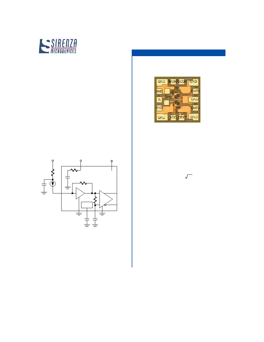
Sirenza Microdevices' SFT-0100 is a high performance
heterojunction bipolar transistor transimpedance amplifier
designed for 10/12.5 Gb/s SONET/SDH applications. The
SFT-0100 uses high F
T
indium gallium phosphide device
technology that delivers hign transimpdeance, large
dynamic range, and a typical bandwidth greater than
10.5GHz.
Performanced is enhanced through the use of a patented
circuit topology that reduces duty cycle distortion under
high photocurrent conditions and allows high transimped-
ance with low DC power to be realized. The SFT-0100 is
supplied in bare die form and includes a current monitor
feature that can be used for fiber alignment or loss of sig-
nal (LOS) detection.
Functional Block Diagram
SFT-0100
Transimpedance Amplifier
Product Features
Applications
�
Low noise InGaP HBT technology
�
Differential transimpedance ~ 2200
�
+5.0V power supply
�
High sensitivity <
�
Adjustable dynamic range
�
Low duty-cycle distortion
�
Differential Outputs
�
Photo current monitor
�
Patented DCDR circuit
�
Backside vias eliminate the need for ground
wirebonds
10pA
Hz
/
�
Optical Receiver Modules
�
XFP, XENPAK, XPAK modules
�
10.7 Gb/s SONET OC-192/SDH STM-64
�
10.3 Gb/s Ethernet Applications
�
12.5 Gb/s SONET with FEC
Product Description
TIA
AMP1
DCDR
Imon
Vcc
Vpin
Rx
C
filter
VOUTP
VOUTN
C
DCDR
C
ext
Transimpedance
Amplifier
Photo-detector
Chip Size: 1000um x 1000um x 100um
522 Almanor Ave., Sunnyvale, CA 94085
Phone: (800) SMI-MMIC
http://www.sirenza.com
2
EDS-102714 Rev. B
Preliminary Data Sheet
SFT-0100 Transimpedance Amplifier
Absolute Maximum Ratings
Parameters
Value
Unit
Supply Current (I
CC
)
60
mA
Device Voltage (V
CC
)
6.0
V
Maximum DC Input Current
5.0
mA
Operating Temperature (T
OP
)
0 to +85
�C
Storage Temperature Range
-40 to +150
�C
Operating Junction Temperature (T
J
)
+150
�C
Product Specifications � Electrical
Parameters
Unit
Min.
Typ.
Max.
Differential Transimpedance
Assume C
D
= 0.26pF, R
D
= 15
, L
INT
= 1.0nH
2000
2200
2400
Transimpedance Bandwidth (3dB)
Assume C
D
= 0.26pF, R
D
= 15
, L
INT
= 1.0nH
GHz
9
10.5
Gain
Single-ended, 50
In/Out
dB
26
27.5
30
Gain Ripple
Single-ended, 50
In/Out
dB
1
S21 3dB Bandwidth
Single-ended, 50
In/Out
GHz
8
9.5
Group Delay Deviation
Single-ended, 50
In/Out, 30kHz - F
C
ps
30
Optical Sensitivity
Assuming 0.8A/W responsivity, measured at 10
-10
BER with a 2
23
-1 PRBS @ 10Gb/s
dBm
-18.5
Optical Overload
Assuming 0.8A/W responsivity, measured at 10
-10
BER with a 2
23
-1 PRBS @ 10Gb/s
mA
2.5 p-p
Input Equivalent Noise Current Density
F = 7GHz
9
Maximum Output Voltage Swing
Single-ended, 50
In/Out
mV p-p
450
Input DC Voltage
V
1.45
Output DC Voltage
50
termination to Vcc
V
4.4
Output Return Loss
Single-ended, 50
In/Out
dB
-10
Supply Voltage
V
4.75
5.0
5.25
Supply Current
Vcc=5.0V
mA
47
52
55
Power Dissipation
mW
260
Input Coupling
AC or DC
DC
Output Type
SE or DF
DF
Output Coupling
AC or DC
AC or DC
Photodiode Current Monitor
Yes
Dynamic Range Adjust
Yes
pA
Hz
/
R=15
C=0.26 pF
L
TIA
Model Used For Transimpedance Calculation
522 Almanor Ave., Sunnyvale, CA 94085
Phone: (800) SMI-MMIC
http://www.sirenza.com
3
EDS-102714 Rev. B
Preliminary Data Sheet
SFT-0100 Transimpedance Amplifier
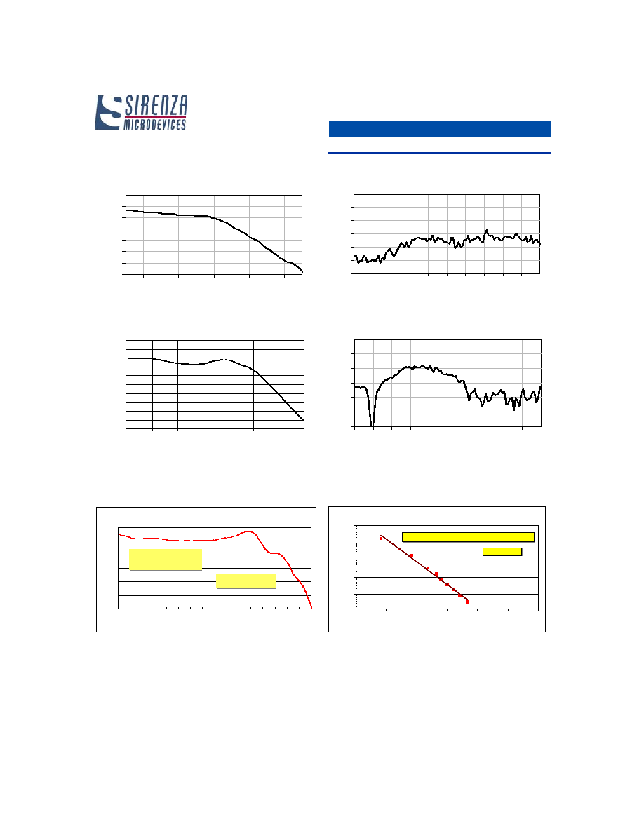
Typical Electrical Performance
Optical Measurement Performance
0
2
4
6
8
10
1 2
14
1 6
18
20
F req u en cy (G H z)
-30
-25
-20
-15
-10
-5
0
S11
(
d
B
)
S 11 vs. F req u e n c y
0
2
4
6
8
10
12
14
16
18
20
F req uency (G Hz)
0
5
10
15
20
25
30
35
S2
1
(d
B
)
S 21 vs. Frequency
Transimpedance Gain
Cpd=0.26pF, Rd=15
, Lwb=1nH
45
47
49
51
53
55
57
59
61
63
65
0
2
4
6
8
10
12
14
Frequency (GHz)
T
r
a
n
si
m
p
ed
a
n
ce
(d
B
o
h
m
s)
0
2
4
6
8
10
12
14
16
18
20
Frequency (G Hz)
-30
-25
-20
-15
-10
-5
0
S2
2
(d
B
)
S22 vs. Frequency
O/E Frequency Response
0
5
10
15
20
25
30
0
2
4
6
8
10
12
14
16
Frequency, (GHz)
R
e
s
ponse
(
d
B
)
f
3dB
= 11.8 GHz
TZ = 3 K
R = 0.8 A/W
Sensitivity Measurement
1.E-11
1.E-10
1.E-09
1.E-08
1.E-07
1.E-06
-20.5
-20.0
-19.5
-19.0
-18.5
-18.0
-17.5
Optical Power (dBm)
BE
R
Sensitivity = -18.8 dBm @ BER = 1E-10
R = 0.8 A/W
Note: All electrical measurements performed using die probe station.
522 Almanor Ave., Sunnyvale, CA 94085
Phone: (800) SMI-MMIC
http://www.sirenza.com
4
EDS-102714 Rev. B
Preliminary Data Sheet
SFT-0100 Transimpedance Amplifier
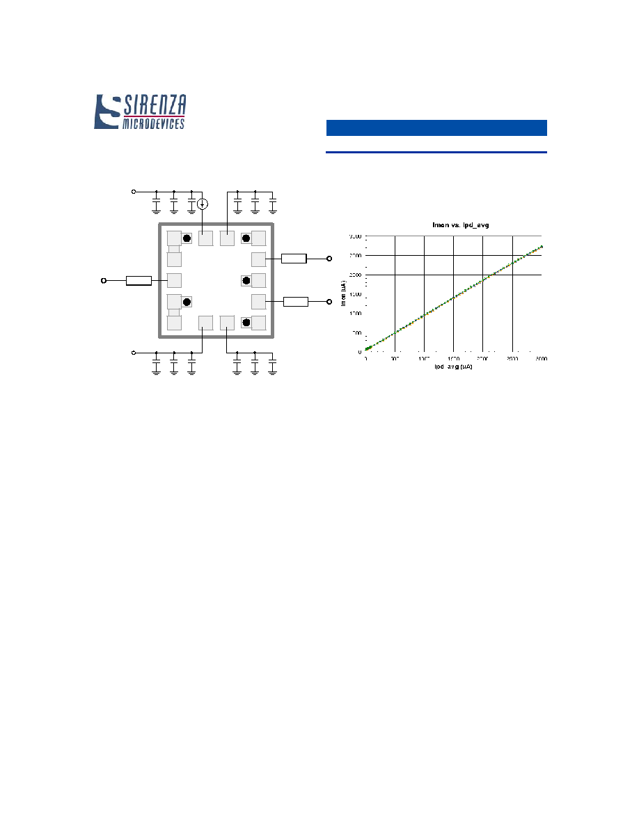
DCDR
IMON
GND
OUT2
GND
OUT1
GND
GND
GND
IN
GND
GND
VCC
CEXT
Zo = 50
Zo = 50
Zo = 50
IN
OUT1
OUT2
100pF
1000pF 0.1uF
100pF
1000pF
0.1uF
Imon
Vcc (5V)
Vcc (5V)
100pF
1000pF 0.1uF
100pF
1000pF
0.1uF
Application Circuit
Description of External Connections and How They Operate
Imon: When tied to the supply voltage through an amme-
ter, the current through the ammeter "Imon" reflects the
average photo diode current. The Imon current will be
approximately the value of the average photo diode cur-
rent and will be directly proportional to this quantity. Imon
can be used for loss of signal detection or photodiode/fiber
alignment in manufacturing. A third function this monitor
can provide is the manual adjustment of the DCDR thresh-
old. With no input photocurrent applied to the TIA, the
Imon will give a finite quiescent current (uA). The finite cur-
rent indicates that the automatic circuit has already started
to turn on. By employing a shunt resistor (20K-200K) on
the C
DCDR
port to ground, this threshold can be reduced
(current can be reduced to a few uA) setting the automatic
circuit for maximum sensitivity and dynamic range.
DCDR(Duty Cycle Distortion Reduction): This feature
compensates for the duty cycle distortion as a result of
high input current seen by the amplifier. As the optical
input power and induced photo current is increased, an
automatic circuit is invoked to prevent distorted operation
in the transistors of the TIA. The threshold input current
where the circuit turns on can be adjusted by employing a
shunt resistor to ground at the DCDR pin. The value of the
shunt resistor can be set between 20K and 200K. The
lower the value, the higher the input current threshold in
which the circuit turns on. In order to optimize for maxi-
mum sensitivity and dynamic range, the Imon current can
be monitored while tuning this shunt resistor. Optimum
sensitivity and dynamic range can be obtained by tuning
the resistor value until only a few uA of Imon current is
observed when there is no optical input power applied.
(Patented)
C
DCDR
: An off chip capacitor is required in order to inte-
grate and produce the automatic circuit control voltage.
C
EXT
: An off chip capacitor sets the lower frequency of
operation for the amplifier. For 30KHz operation and
below, a 0.1uF capacitor is required.