
Contents
Features.............................................................. 1
Applications......................................................... 1
Pin Assignment ................................................... 1
Block Diagram..................................................... 1
Selection Guide................................................... 2
Output Configurations ......................................... 3
Advantage over the S-808 Series........................ 3
Absolute Maximum Ratings................................. 4
Electrical Characteristics ..................................... 5
Test Circuits ........................................................ 9
Technical Terms ................................................. 10
Standard Circuit .................................................. 11
Operation ............................................................ 12
Dimensions ......................................................... 14
Taping ................................................................ 14
Marking ............................................................... 15
Characteristics (typical characteristics) ............... 16
Application Circuit Examples ............................... 23
Notes ............................................................... 23

Seiko Instruments Inc.
1
BUILT-IN DELAY CIRCUIT HIGH-PRECISION VOLTAGE DETECTOR
S-809 Series
The S-809 Series is a high-precision voltage detector developed using
CMOS process. The detection voltage is fixed internally, with an
accuracy of
±
2.0%. Attachment of an external capacitor can delay the
release signal. Two output types, Nch open-drain and CMOS output,
are available.
Features
Applications
·
Ultra-low current consumption
·
Battery checker
1.0
µ
A typ. (V
DD
=2.0 V)
·
Power failure detector
; Products with a detection voltage of 1.4V or less
·
Power monitor for portable equipment such as
1.2
µ
A typ. (V
DD
=3.5 V)
pagers, electric calculators, electric notes and
; Products with a detection voltage of 1.5V or more
remote controllers
·
High-precision detection voltage
·
Constant voltage power monitor for cameras,
±
2.0%
video equipment and communication devices
·
Low operating voltage
·
Power monitor for microcomputers and reset for
0.80 to 6.0 V
CPUs
; Products with detection voltage of 1.4,uor less
0.95 to 10.0,u
; Products with detection voltage of 1.5,uor more
·
Hysteresis characteristics
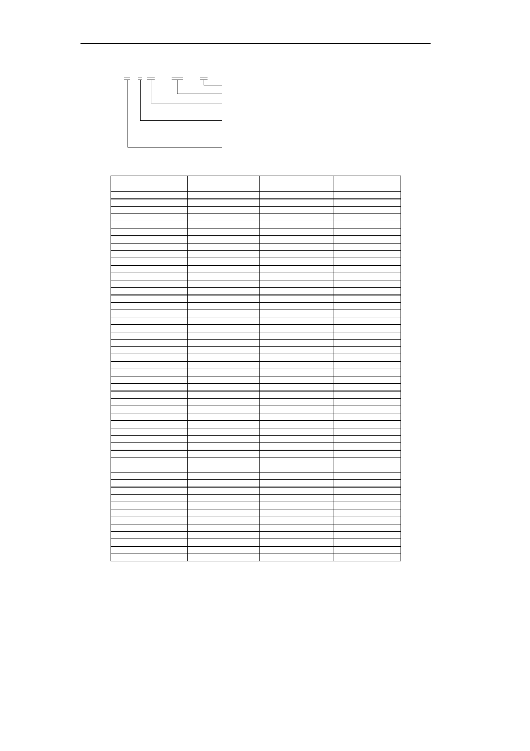
Pin Assignment
5% typ
·
Detection voltage
1.1 to 6.0 V
(0.1V step)
·
Nch open-drain active low and CMOS active low output
·
SOT-23-5 Very-small plastic package
Figure 1
Block Diagram
(1) Nch open-drain active low output
(2) CMOS active low output
Figure 2
1 OUT
2 V
DD
3 V
SS
4 NC
5 C
D
SOT-23-5
Top view
1
2
3
5
4
2
5
3
1
Delay
circuit
OUT
C
D
V
REF
V
SS
V
DD
*
*
*Parasitic diode
2
5
3
1
Delay
circuit
OUT
C
D
V
REF
V
SS
V
DD
*
BUILT-IN DELAY CIRCUIT HIGH-PRECISION VOLTAGE DETECTOR
S-809 Series
2
Seiko Instruments Inc.
Selection Guide
S
-
80915 AN MP
-
DDC
-
T2
Directions of the IC for taping specifications
Product name (abbreviation)
Package name (abbreviation)
MP:SOT-23-5
Output type
N:Nch open-drain (active low output)
L:CMOS (active low output)
Detection voltage rank
Table 1
Detection voltage range (V)
Hysteresis width
V
HYS
typ.(V)
Nch Open Drain(Low)
CMOS Output(Low)
1.1V
±
2.0%
0.055
S-80911ANMP-D71-T2
S-80911ALMP-D51-T2
1.2V
±
2.0%
0.060
S-80912ANMP-D72-T2
S-80912ALMP-D52-T2
1.3V
±
2.0%
0.065
S-80913ANMP-DDA-T2
S-80913ALMP-DAA-T2
1.4V
±
2.0%
0.070
S-80914ANMP-DDB-T2
S-80914ALMP-DAB-T2
1.5V
±
2.0%
0.075
S-80915ANMP-DDC-T2
S-80915ALMP-DAC-T2
1.6V
±
2.0%
0.080
S-80916ANMP-DDD-T2
S-80916ALMP-DAD-T2
1.7V
±
2.0%
0.085
S-80917ANMP-DDE-T2
S-80917ALMP-DAE-T2
1.8V
±
2.0%
0.090
S-80918ANMP-DDF-T2
S-80918ALMP-DAF-T2
1.9V
±
2.0%
0.095
S-80919ANMP-DDG-T2
S-80919ALMP-DAG-T2
2.0V
±
2.0%
0.100
S-80920ANMP-DDH-T2
S-80920ALMP-DAH-T2
2.1V
±
2.0%
0.105
S-80921ANMP-DDJ-T2
S-80921ALMP-DAJ-T2
2.2V
±
2.0%
0.110
S-80922ANMP-DDK-T2
S-80922ALMP-DAK-T2
2.3V
±
2.0%
0.115
S-80923ANMP-DDL-T2
S-80923ALMP-DAL-T2
2.4V
±
2.0%
0.120
S-80924ANMP-DDM-T2
S-80924ALMP-DAM-T2
2.5V
±
2.0%
0.125
S-80925ANMP-DDN-T2
S-80925ALMP-DAN-T2
2.6V
±
2.0%
0.130
S-80926ANMP-DDP-T2
S-80926ALMP-DAP-T2
2.7V
±
2.0%
0.135
S-80927ANMP-DDQ-T2
S-80927ALMP-DAQ-T2
2.8V
±
2.0%
0.140
S-80928ANMP-DDR-T2
S-80928ALMP-DAR-T2
2.9V
±
2.0%
0.145
S-80929ANMP-DDS-T2
S-80929ALMP-DAS-T2
3.0V
±
2.0%
0.150
S-80930ANMP-DDT-T2
S-80930ALMP-DAT-T2
3.1V
±
2.0%
0.155
S-80931ANMP-DDV-T2
S-80931ALMP-DAV-T2
3.2V
±
2.0%
0.160
S-80932ANMP-DDW-T2
S-80932ALMP-DAW-T2
3.3V
±
2.0%
0.165
S-80933ANMP-DDX-T2
S-80933ALMP-DAX-T2
3.4V
±
2.0%
0.170
S-80934ANMP-DDY-T2
S-80934ALMP-DAY-T2
3.5V
±
2.0%
0.175
S-80935ANMP-DDZ-T2
S-80935ALMP-DAZ-T2
3.6V
±
2.0%
0.180
S-80936ANMP-DD0-T2
S-80936ALMP-DA0-T2
3.7V
±
2.0%
0.185
S-80937ANMP-DD1-T2
S-80937ALMP-DA1-T2
3.8V
±
2.0%
0.190
S-80938ANMP-DD2-T2
S-80938ALMP-DA2-T2
3.9V
±
2.0%
0.195
S-80939ANMP-DD3-T2
S-80939ALMP-DA3-T2
4.0V
±
2.0%
0.200
S-80940ANMP-DD4-T2
S-80940ALMP-DA4-T2
4.1V
±
2.0%
0.205
S-80941ANMP-DD5-T2
S-80941ALMP-DA5-T2
4.2V
±
2.0%
0.210
S-80942ANMP-DD6-T2
S-80942ALMP-DA6-T2
4.3V
±
2.0%
0.215
S-80943ANMP-DD7-T2
S-80943ALMP-DA7-T2
4.4V
±
2.0%
0.220
S-80944ANMP-DD8-T2
S-80944ALMP-DA8-T2
4.5V
±
2.0%
0.225
S-80945ANMP-DD9-T2
S-80945ALMP-DA9-T2
4.6V
±
2.0%
0.230
S-80946ANMP-DJA-T2
S-80946ALMP-DEA-T2
4.7V
±
2.0%
0.235
S-80947ANMP-DJB-T2
S-80947ALMP-DEB-T2
4.8V
±
2.0%
0.240
S-80948ANMP-DJC-T2
S-80948ALMP-DEC-T2
4.9V
±
2.0%
0.245
S-80949ANMP-DJD-T2
S-80949ALMP-DED-T2
5.0V
±
2.0%
0.250
S-80950ANMP-DJE-T2
S-80950ALMP-DEE-T2
5.1V
±
2.0%
0.255
S-80951ANMP-DJF-T2
S-80951ALMP-DEF-T2
5.2V
±
2.0%
0.260
S-80952ANMP-DJG-T2
S-80952ALMP-DEG-T2
5.3V
±
2.0%
0.265
S-80953ANMP-DJH-T2
S-80953ALMP-DEH-T2
5.4V
±
2.0%
0.270
S-80954ANMP-DJJ-T2
S-80954ALMP-DEJ-T2
5.5V
±
2.0%
0.275
S-80955ANMP-DJK-T2
S-80955ALMP-DEK-T2
5.6V
±
2.0%
0.280
S-80956ANMP-DJL-T2
S-80956ALMP-DEL-T2
5.7V
±
2.0%
0.285
S-80957ANMP-DJM-T2
S-80957ALMP-DEM-T2
5.8V
±
2.0%
0.290
S-80958ANMP-DJN-T2
S-80958ALMP-DEN-T2
5.9V
±
2.0%
0.295
S-80959ANMP-DJP-T2
S-80959ALMP-DEP-T2
6.0V
±
2.0%
0.300
S-80960ANMP-DJQ-T2
S-80960ALMP-DEQ-T2

BUILT-IN DELAY DIRCUIT HIGH-PRECISION VOLTAGE DETECTOR
S-809 Series
Seiko Instruments Inc.
3
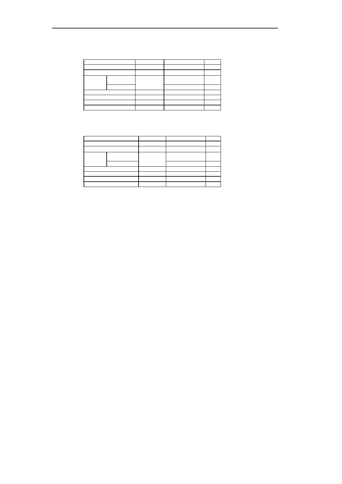
Output Configurations
1.
S-809 Series model numbering system
Nch open-drain
(
"
L
"
reset type)
CMOS output
(
"
L
"
reset type)
S-809 Series
"
N
"
is the last letter of the
model number.
e.g. S-80915AN
"
L
"
is the last letter of the
model number.
e.g. S-80915AL
2.
Output configurations and their implementation
Implementation
Nch(
"
L
"
)
CMOS(
"
L
"
)
With different power supplies
Yes
No
With active low reset CPUs
Yes
Yes
With active high reset CPUs
No
No
With voltage divider variable resistors
Yes
No
Example with two power supplies
Examples with one power supply
V
SS
OUT
CPU
V
DD
2
V
DD
1
V/D
Nch
C
D
V
SS
OUT
CPU
V
DD
V/D
CMOS
C
D
V
SS
OUT
CPU
V
DD
V/D
Nch
C
D
Figure 3
Advantage over the S-808 Series
1.
Built-In delay circuit
Delay time setting by an additional external capacitor:
The S-809 can easily delay an release signal by attachment of an external capacitor with built-In delay circuit.
This results in an advantage of parts reduction over the S-808 Series.
BUILT-IN DELAY CIRCUIT HIGH-PRECISION VOLTAGE DETECTOR
S-809 Series
4
Seiko Instruments Inc.
Absolute Maximum Ratings
1.
Products with a Detection voltage of 1.4 or less.
(Unless otherwise specified: Ta=25
°
C)
Parameter
Symbol
Ratings
Unit
Power supply voltage
V
DD
-
V
SS
8
V
C
D
terminal Input voltage
V
CD
V
SS
-0.3 to V
DD
+0.3
V
Output
voltage
Nch
open-drain
V
OUT
V
SS
-0.3 to 8
V
CMOS
V
SS
-0.3 to V
DD
+0.3
V
Output current
I
OUT
50
mA
Power dissipation
Pd
150
mW
Operating temperature
Topr
-
40 to +85
°
C
Storage temperature
Tstg
-
40 to +125
°
C
2.
Products with a Detection voltage of 1.5 or more.
(Unless otherwise specified: Ta=25)
Parameter
Symbol
Ratings
Unit
Power supply voltage
V
DD
-
V
SS
12
V
C
D
terminal Input voltage
V
CD
V
SS
-0.3 to V
DD
+0.3
V
Output
voltage
Nch
open-drain
V
OUT
V
SS
-0.3 to 12
V
CMOS
V
SS
-0.3 to V
DD
+0.3
V
Output current
I
OUT
50
mA
Power dissipation
Pd
150
mW
Operating temperature
Topr
-
40 to +85
°
C
Storage temperature
Tstg
-
40 to +125
°
C
Note:
This IC has a built-in protection circuit for static electricity, however, prevent contact with a large static
electricity or electrostatic voltage which exceeds the performance of the protection circuit.