
Contents
Features.............................................................. 1
Block Diagram..................................................... 2
Pin Description .................................................... 3
Pad Assignment.................................................. 5
Pad Coordinates ................................................. 6
Function Explanation........................................... 7
Instruction Explanation ........................................ 17
Instruction List..................................................... 27
Operation Description ......................................... 29
Examples of Connection to LCD Panel ............... 35
Examples of LCD Drive Output Waveform .......... 37
External BiasResistor vs LCD Drive Waveform... 38
Absolute Maximum Ratings................................. 39
DC Characteristics .............................................. 39
Current Consumption Measurement Examples ... 43
Timing Characteristics......................................... 44
Examples Application Circuit ............................... 47

Seiko Instruments Inc.
1
LCD Controller-Driver
S-4561A
The S-4561A is a 17-common x 60-segment output character LCD
controller-driver with built-in serial and parallel interfaces. The S-4561A
incorporates CGROM, making character display possible. Independently
of the CPU, display on the LCD panel is executed via the internal
oscillating circuit or clock input. The S-4561A has a wide variety of
command instructions which minimize the load of the CPU. It also
features a wide voltage range, low power consumption, and it is provided
with a power save function, making the S-4561A a suitable display
device for applications in portable electronics.
T
Features
·
Display Area
·
Duty Cycle: 1/17
5-dot font
·
Internal LCD Drive Bias Voltage Generator
12-column x 2-line (+4 columns)
Internal Bias Resistor :
24-column x 1-line (+8 columns)
Command selection
1/5 or 1/4 bias
6-dot font
External Bias Resistor :
10-column x 2-line (+6 columns)
Free setting of 1/2 bias or more
20-column x 1-line (+12 columns)
·
Normal Instructions
Values in parentheses indicate the number of columns
Display Clear, Cursor Home, Display
outside the display area.
ON/OFF, Display Character Blink,
·
Icon Display
Cursor Shift, Display Shift, Cursor
60 icons (max.)
ON/OFF
Icons can be displayed on the upper and lower panel.
·
Extended Instructions
·
Fonts: 5-dot display mode and 6-dot display mode
Contrast Adjustment, Smooth Scroll
·
Interface
Control, Icon Control, Icon Blink, Bias
4-bit, 8-bit high-speed parallel interface (80-/68-Family CPU)
Resistor Select, Change of Number of
Serial interface
Display Columns, Power Save, Icon Only
·
Driver Output
Display, Booster Drive Frequency Select
60 segments
·
Reset Circuit : Hardware Reset
16 commons+ Icon common :
·
Internal Booster :
Dual Booster
·
Character Generator ROM (CGROM)
·
Power Supply Voltage Range
9600 bits, 5
×
8 bits character font, 240 characters
Logic Power :
2.4 V to 5.5 V
·
Character Generator RAM (CGRAM)
LCD Drive Power : 2.7 V to 6.5 V
8 character x 5 x 8=320 bits
·
Low Current Consumption :
·
Display Data RAM (DDRAM)
Approx. 0
µ
A (during power save
operation)
2 lines x 16 characters=2 x 16 x 8=256 bits
·
Delivered on gold bump bare chips,
(4 characters are displayed outside the display area)
·
Notice that isolation of the IC from light exposure
·
Display Clock
is not taken into account for this IC design.
Either internal CR oscillating circuit or external clock input :
Be sure to take measures not to expose light to
CR oscillation: 34 kHz
the surface, back, or side of the IC in order to
(Frame Frequency=76.9 Hz)
prevent this IC from malfunctioning.
LCD Controller-Driver
S-4561A
2
Seiko Instruments Inc.
T
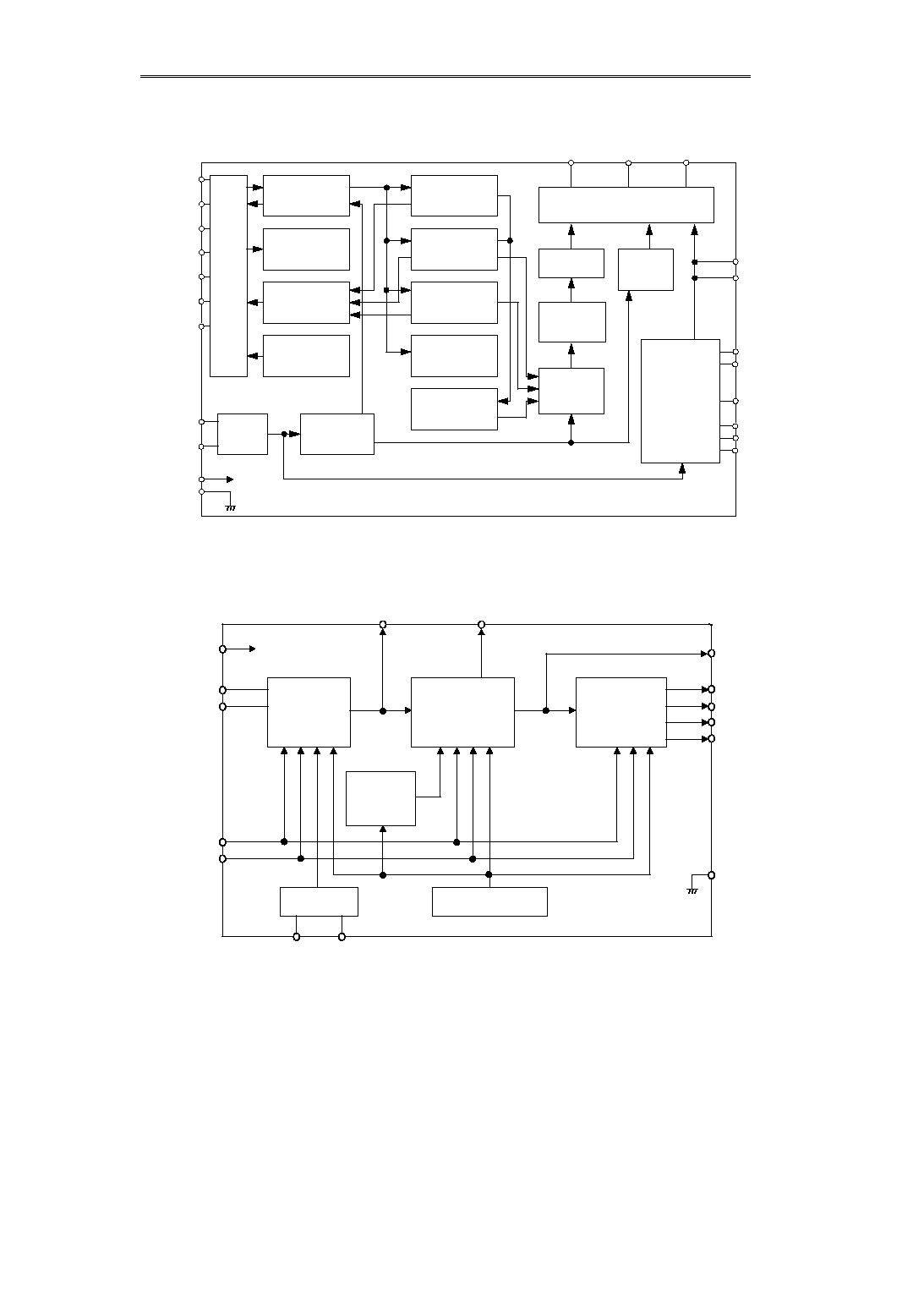
Block Diagram
1. Block Overview
Figure 1 Block Diagram
2. LCD Power Supply Circuit
Figure 2 LCD Power Supply Circuit
SEG1 to 60
COMICN1, 2
LCD Driver
V1 to V4
C1-
C1+
V
OUT
V
CNT
FNC1
COM1 to 16
Latch
Circuit
Common
Counter
LCD
Power Supply
Circuit
Parallel
Conversion
Circuit
FNC2
Cursor
Blink
Circuit
Display RAM
8 bits
×
32
CGRAM
5 bits
×
64
Icon RAM
5 bits
×
12
Icon Blink RAM
5 bits
×
12
CGROM
5 bits
×
240
×
8
Address
Counter
Instruction
Decoder
Data
Holder
BUSY
Timing
Control
Circuit
Osc.
Circuit
MPU
Inter-
face
RS
E
R/WX
RESX
P/SX
DB
(0-7)
OSC1
OSC2
V
DD
V
SS
V
LCD
C86
Voltage Regulator/
LCD Voltage
Command
LCD Bias
Resistor/
Voltage Follower
Booster
Standard
Voltage
Circuit
CR Oscillating
Circuit
MPU Interface
OSC1
OSC2
V
SS
V
1
V
2
V
3
V
4
V
CNT
V
OUT
V
DD
C1+
C1-
FNC1
FNC2
V
LCD
LCD Controller-Driver
S-4561A
Seiko Instruments Inc.
3
T
T
Pin Description
1.
Logic Power Supply Pins
Table 1 Logic Power Supply Pins
Pin No.
Pin Name
Description
47
V
SS
Negative Power Pin: Usually connected to 0 V (GND)
33
V
DD
Positive Power Pin: Usually connected to+3 V
2.
Control Pins
Table 2 Control Pins
Pin No.
Pin Name
Description
7, 9
11, 13
15, 17
19, 21
DB0 to DB7
·
When an 8-bit parallel interface is selected:
8-Bit Parallel Data Bus 3-State Input/Output Pin
·
When a 4-bit parallel interface is selected:
DB0 to DB3 : Open
DB4 to DB7 : 4-Bit Parallel Data Bus 3-State Input/Output Pins
·
When a serial interface is selected:
DB0
: Serial Data Input Pin
DB1
: Clock Input Pin
DB2 to DB7 : Open
25
R/WX
·
When a 4-bit/8-bit parallel interface is selected:
68-Family MPU Read/Write Signal Input Pin
R/WX=
"
H
"
:
Read
R/WX=
"
L
"
:
Write
80-Family MPU:
Write Signal Input Pin
Active
"
L
"
Data Bus Input State
·
When a serial interface is selected:
High Impedance
27
P/SX
·
Parallel/Serial Interface Changeover Pin
P/SX=
"
H
"
: 4-Bit/8-Bit Parallel Interface
P/SX=
"
L
"
: Serial Interface
29
RS
·
When 4-bit/8-bit parallel interface is selected:
Register Select Signal Input Pin
RS=
"
0
"
:
Instruction Register Write
Each Address Counter Read
BUSY Flag Read
RS=
"
1
"
:
Data Register Write/Read
·
When a serial interface is selected:
RS=
"
0
"
:
Instruction Register Write
RS=
"
1
"
:
Data Register Write
31
E
·
When a 4-bit/8-it parallel interface is selected:
68-Family MPU Enable Clock Signal Input Pin
Active
"
H
"
80-Family MPU Read Signal Input Pin
Active
"
L
"
Data Bus Output State
·
When a serial interface is selected:
Chip-Select Input Pin
E=
"
L
"
:
Active
23
RESX
·
Reset Input Pin
Active
"
L
"
Internal Pullup Register
39
C86
·
When 4-bit/8-bit parallel interface is selected:
C86=
"
H
"....................
68-Family Interface
C86=
"
L
" ....................
80-Family Interface
·
When a serial interface is selected:
Don't care.
LCD Controller-Driver
S-4561A
4
Seiko Instruments Inc.
3.
CR Oscillating Circuit Input/Output Pins
Table 3 CR Oscillating Circuit Input/Output Pins
Pin No.
Pin Name
Description
5
OSC2
CR Oscillating Circuit Output Pin: Connects oscillating resistor Rf; while an external clock is
being used,
"
Open.
"
3
OSC1
CR Oscillating Circuit Input Pin: Connects oscillating resistor Rf; An external clock can be input.
4.
LCD Drive Voltage Pins
Table 4 LCD Drive Voltage Pins
5. Driver Output Pins
Table 5 Driver Output Pins
6. Other Pins
Table 6 Logic Power Supply Pins
Pin No.
Pin Name
Description
35
FNC2
LCD Power Circuit Operation Control Pin 2
37
FNC1
LCD Power Circuit Operation Control Pin 1
49
VOUT
Booster Drive Voltage Output Pin
51
C1-
1st Boosting Negative Side Connection Pin
53
C1+
1st Boosting Positive Side Connection Pin
59
VCNT
LCD Power Supply Voltage Control Pin
65
V
LCD
LCD Drive Voltage Input/Output Pin
67
69
71
73
V1
V2
V3
V4
LCD Drive Bias Voltage Pin
While an internal LCD power supply circuit is being used, outputs the LCD
drive bias voltage.
1/4-Bias
1/5-Bias
V1
3/4
×
V
LCD
4/5
×
V
LCD
V2
2/4
×
V
LCD
3/5
×
V
LCD
V3
2/4
×
V
LCD
2/5
×
V
LCD
V4
1/4
×
V
LCD
1/5
×
V
LCD
While an external LCD power supply circuit is being used, inputs the LCD drive bias
voltage.
V
LCD
V1, V2, V3, V4
VSS
V
LCD
V
DD
Pin No.
Pin Name
Description
91 to 150
SEG1
to
SEG60
Segment Drive Output Pins
76 to 83
159 to 166
COM1 to
COM16
Common Drive Output Pins
75
COMICN1
Common Drive Output Pins for Icon
158
COMICN2
COMICN1 and 2 output the same phase waveform.
Pin No.
Pin Name
Description
Dummy
Dummy Pin
Insulated from the inside of the IC.
45
TEST0
Pins for IC delivery inspection:
43
TEST1
Cannot be wired to the outside.
41
TEST2
When in actual use,
"
Open.
"
57
TEST3
63
TEST4
LCD Controller-Driver
S-4561A
Seiko Instruments Inc.
5
T
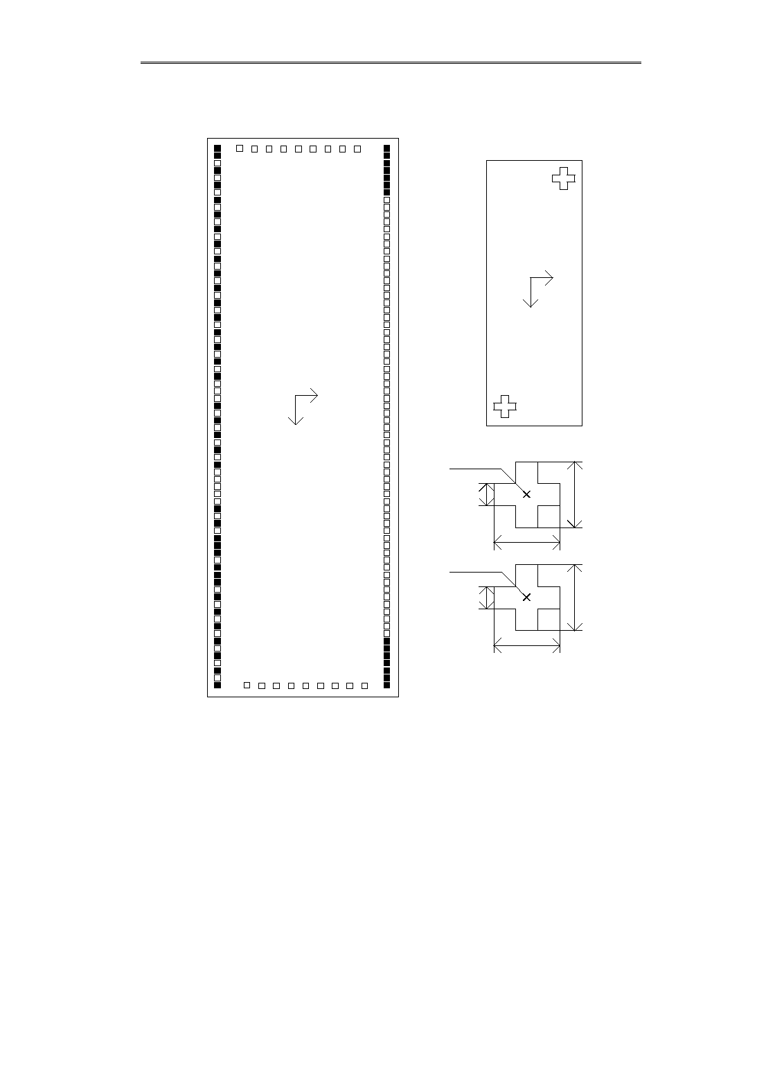
Pad Assignment
75
A
·
Chip size:
7.65
×
2.00 mm
·
Gold bump size: 70
×
94
µ
m
·
Gold bump height:
22
±
7
µ
m
·
Pad
pitch
100
µ
m
·
Chip thickness:
400
±
30
µ
m
A
B
Chip Identification Mark
(The identification marks are larger than the actual scaling.)
X
Gold bump size
70 x 94
µ
m
Pad pitch
100
µ
m
(-3660, 625)
0.168
C
O
M
9
1
2
3
4
5
6
7
8
9
10
11
12
13
14
15
16
17
18
19
20
21
22
23
24
25
26
27
28
29
30
31
32
33
34
35
36
37
38
39
40
41
42
43
44
45
46
47
48
49
50
51
52
53
54
55
56
57
58
59
60
61
62
63
64
65
66
67
68
69
70
71
72
73
74
Dummy
OSC1
76
77
78
79
80
81
82
83
Dummy
Dummy
OSC2
Dummy
DB7
Dummy
C
O
M
10
C
O
M
11
C
O
M
12
C
O
M
13
C
O
M
14
C
O
M
15
C
O
M
16
C
O
M
I
C
N
2
C
O
M
8
C
O
M
1
C
O
M
2
C
O
M
3
C
O
M
4
C
O
M
5
C
O
M
6
C
O
M
7
C
O
M
I
C
N
1
DB6
Dummy
DB5
Dummy
DB4
Dummy
DB3
Dummy
DB2
Dummy
DB1
Dummy
DB0
Dummy
RESX
Dummy
R/WX
Dummy
P/SX
Dummy
RS
Dummy
E
Dummy
VDD
VDD
FNC2
Dummy
FNC1
Dummy
C86
Dummy
TEST 2
Dummy
TEST 1
Dummy
TEST 0
VSS
VSS
VSS
VOUT
Dummy
157
156
155
154
153
152
151
150
149
148
147
146
145
144
143
142
141
140
139
138
137
136
135
134
133
132
131
130
129
128
127
126
125
124
123
122
121
120
119
118
117
116
115
114
113
112
111
110
109
108
107
106
105
104
103
102
101
100
99
98
97
96
95
94
93
92
91
90
89
88
87
86
85
84
C1 -
Dummy
C1+
Dummy
Dummy
Dummy
TEST 3
Dummy
Dummy
VCNT
Dummy
TEST 4
Dummy
VLCD
Dummy
V1
Dummy
V2
Dummy
V3
Dummy
V4
Dummy
Dummy
SEG60
SEG59
SEG58
SEG57
SEG56
SEG55
SEG54
Dummy
Dummy
Dummy
Dummy
Dummy
Dummy
Dummy
SEG53
SEG52
SEG51
SEG50
SEG49
SEG48
SEG47
SEG46
SEG45
SEG44
SEG43
SEG42
SEG41
SEG40
SEG39
SEG38
SEG37
SEG36
SEG35
SEG34
SEG33
SEG32
SEG31
SEG30
SEG29
SEG28
SEG27
SEG26
SEG25
SEG24
SEG23
SEG22
SEG21
SEG20
SEG19
SEG18
SEG17
SEG16
SEG15
SEG14
SEG13
SEG12
SEG11
SEG10
SEG9
SEG8
SEG7
SEG6
SEG5
SEG4
SEG3
SEG2
SEG1
Dummy
Dummy
Dummy
Dummy
Dummy
Dummy
Dummy
Y
X
0.168
0.056
B
(3669, -590)
0.15
0.15
0.05
166
165
164
163
162
161
160
159
158
Y
LCD Controller-Driver
S-4561A
6
Seiko Instruments Inc.
T
Pad Coordinates
No.
Symbol
X
Y
No.
Symbol
X
Y
No.
Symbol
X
Y
1
Dummy
-3700.5
-863.5
57
TEST3
1950
-863.5
113
SEG23
750
863.5
2
Dummy
-3550
-863.5
58
Dummy
2050
-863.5
114
SEG24
650
863.5
3
OSC1
-3450
-863.5
59
Dummy
2150
-863.5
115
SEG25
550
863.5
4
Dummy
-3350
-863.5
60
Dummy
2250
-863.5
116
SEG26
450
863.5
5
OSC2
-3250
-863.5
61
VCNT
2350
-863.5
117
SEG27
350
863.5
6
Dummy
-3150
-863.5
62
Dummy
2450
-863.5
118
SEG28
250
863.5
7
DB7
-3050
-863.5
63
TEST4
2550
-863.5
119
SEG29
150
863.5
8
Dummy
-2950
-863.5
64
Dummy
2650
-863.5
120
SEG30
50
863.5
9
DB6
-2850
-863.5
65
VLCD
2750
-863.5
121
SEG31
-50
863.5
10
Dummy
-2750
-863.5
66
Dummy
2850
-863.5
122
SEG32
-150
863.5
11
DB5
-2650
-863.5
67
V1
2950
-863.5
123
SEG33
-250
863.5
12
Dummy
-2550
-863.5
68
Dummy
3050
-863.5
124
SEG34
-350
863.5
13
DB4
-2450
-863.5
69
V2
3150
-863.5
125
SEG35
-450
863.5
14
Dummy
-2350
-863.5
70
Dummy
3250
-863.5
126
SEG36
-550
863.5
15
DB3
-2250
-863.5
71
V3
3350
-863.5
127
SEG37
-650
863.5
16
Dummy
-2150
-863.5
72
Dummy
3450
-863.5
128
SEG38
-750
863.5
17
DB2
-2050
-863.5
73
V4
3550
-863.5
129
SEG39
-850
863.5
18
Dummy
-1950
-863.5
74
Dummy
3700.5
-863.5
130
SEG40
-950
863.5
19
DB1
-1850
-863.5
75
COMICN1
3688.5
-400
131
SEG41
-1050
863.5
20
Dummy
-1750
-863.5
76
COM1
3688.5
-300
132
SEG42
-1150
863.5
21
DB0
-1650
-863.5
77
COM2
3688.5
-200
133
SEG43
-1250
863.5
22
Dummy
-1550
-863.5
78
COM3
3688.5
-100
134
SEG44
-1350
863.5
23
RESX
-1450
-863.5
79
COM4
3688.5
0
135
SEG45
-1450
863.5
24
Dummy
-1350
-863.5
80
COM5
3688.5
100
136
SEG46
-1550
863.5
25
R/WX
-1250
-863.5
81
COM6
3688.5
200
137
SEG47
-1650
863.5
26
Dummy
-1150
-863.5
82
COM7
3688.5
300
138
SEG48
-1750
863.5
27
P/SX
-1050
-863.5
83
COM8
3688.5
400
139
SEG49
-1850
863.5
28
Dummy
-950
-863.5
84
Dummy
3700.5
863.5
140
SEG50
-1950
863.5
29
RS
-850
-863.5
85
Dummy
3550
863.5
141
SEG51
-2050
863.5
30
Dummy
-750
-863.5
86
Dummy
3450
863.5
142
SEG52
-2150
863.5
31
E
-650
-863.5
87
Dummy
3350
863.5
143
SEG53
-2250
863.5
32
Dummy
-550
-863.5
88
Dummy
3250
863.5
144
SEG54
-2350
863.5
33
VDD
-450
-863.5
89
Dummy
3150
863.5
145
SEG55
-2450
863.5
34
VDD
-350
-863.5
90
Dummy
3050
863.5
146
SEG56
-2550
863.5
35
FNC2
-250
-863.5
91
SEG1
2950
863.5
147
SEG57
-2650
863.5
36
Dummy
-150
-863.5
92
SEG2
2850
863.5
148
SEG58
-2750
863.5
37
FNC1
-50
-863.5
93
SEG3
2750
863.5
149
SEG59
-2850
863.5
38
Dummy
50
-863.5
94
SEG4
2650
863.5
150
SEG60
-2950
863.5
39
C86
150
-863.5
95
SEG5
2550
863.5
151
Dummy
-3050
863.5
40
Dummy
250
-863.5
96
SEG6
2450
863.5
152
Dummy
-3150
863.5
41
TEST2
350
-863.5
97
SEG7
2350
863.5
153
Dummy
-3250
863.5
42
Dummy
450
-863.5
98
SEG8
2250
863.5
154
Dummy
-3350
863.5
43
TEST1
550
-863.5
99
SEG9
2150
863.5
155
Dummy
-3450
863.5
44
Dummy
650
-863.5
100
SEG10
2050
863.5
156
Dummy
-3550
863.5
45
TEST0
750
-863.5
101
SEG11
1950
863.5
157
Dummy
-3700.5
863.5
46
VSS
850
-863.5
102
SEG12
1850
863.5
158
COMICN2
-3688.5
400
47
VSS
950
-863.5
103
SEG13
1750
863.5
159
COM16
-3688.5
300
48
VSS
1050
-863.5
104
SEG14
1650
863.5
160
COM15
-3688.5
200
49
VOUT
1150
-863.5
105
SEG15
1550
863.5
161
COM14
-3688.5
100
50
Dummy
1250
-863.5
106
SEG16
1450
863.5
162
COM13
-3688.5
0
51
C1-
1350
-863.5
107
SEG17
1350
863.5
163
COM12
-3688.5
-100
52
Dummy
1450
-863.5
108
SEG18
1250
863.5
164
COM11
-3688.5
-200
53
C1+
1550
-863.5
109
SEG19
1150
863.5
165
COM10
-3688.5
-300
54
Dummy
1650
-863.5
110
SEG20
1050
863.5
166
COM9
-3688.5
-400
55
Dummy
1750
-863.5
111
SEG21
950
863.5
56
Dummy
1850
-863.5
112
SEG22
850
863.5
LCD Controller-Driver
S-4561A
Seiko Instruments Inc.
7
Table 8 Chip Identification Mark Coordinates
Chip Identification
Mark
X-Coordinates
Y-Coordinates
A
B
- 3660
3669
625
- 590
s
Function Explanation
1.
Interface
Serial and parallel interfaces are built in. Either one can be selected by changing over the P/SX terminal. The parallel
interface can respond to both 4- and 8-bit parallel data transmission. Namely, data is transmitted once in the 8-bit interface
or twice in the 4-bit interface. The CPU interfaces with respective instruction codes and several kinds of data via the
instruction decoder and the data holder.
Data is read from each memory via the data holder. Through the ADDRESS SETTING Command, the contents of the
memory are read once into the data holder, and are output through the next READ command. Then, the next data is read
into the data holder.
Parallel and serial interfaces execute and finish all instructions within the Enable or Clock cycle specified in accordance with
timing characteristics. Because the
"
BUSY
"
state is cleared within the cycle time, instructions can be executed in succession
without confirming the
"
BUSY.
"
1.1 Parallel Interface
The parallel interface is engaged when the P/SX terminal is
"
H.
"
Connect and fix the P/SX terminal to VDD.
Table 9 Interface
Figure 3 8-Bit Length Parallel Interface (68-Family CPU)
Figure 4 8-Bit Length Parallel Interface (80-Family CPU)
Pin Name
C86=0: 80-Family MPU
C86=1: 68-Family MPU
RS
RS
RS
E
RD
E
R/WX
WR
R/WX
DB(7:0)
DB(7:0)
DB(7:0)
RS
E
R/WX
DB0 to DB7
[Example: 8-Bit Length Parallel Interface] (68-Family CPU)
Instruction
Data Write
Address
Data
Instruction
Write
Data
Write
Address
Read
Data
Read
RS
E (RD)
R/WX (WR)
DB0 to DB7
[Example: 8-Bit Length Parallel Interface] (80-Family CPU)
Instruction
Data Write
Address
Data
Write
Instruction
Data
Write
Address
Read
Data
Read
LCD Controller-Driver
S-4561A
8
Seiko Instruments Inc.
Figure 5 4-Bit Length Parallel Interface (68-Family CPU)
Remarks:
R
In case of a 4-bit length interface, data is transmitted through the four buses DB4 to DB7 (buses DB0 to DB3
are not used. Set DB0 to DB3
"
Open
"
).
R
The data transmission to the CPU is completed by transmitting 4-bit data twice. The data transmission is
executed in the order from upper 4 bits to lower 4 bits. The upper 4 bits of data immediately after the output
level of the RS pin changes are transmitted. Leave the RS pin unchanged until lower bits finish the data
transmission.
E
RS
[Example: 4-Bit Length Parallel Interface] (68-Family CPU)
I3
I7
I2
I6
I1
I5
AC3
AC2
AC1
AC0
D7
D6
D5
D4
Busy
D3
0
D2
AC5
D1
AC4
D0
I0
I4
Upper
Lower
Upper
Upper
Lower
Lower
R/WX
DB7
DB6
DB5
DB4
BUSY Flag, Address Counter Read
Data Read
Write Instruction
E (RD)
RS
I3
I7
I2
I6
I1
I5
AC3
AC2
AC1
AC0
D7
D6
D5
D4
Busy
D3
0
D2
AC5
D1
AC4
D0
I0
I4
Upper
Lower
Upper
Upper
Lower
Lower
R/WX (WR)
DB7
DB6
DB5
DB4
Write Instruction
Data Read
BUSY Flag, Address Counter Read
[Example: 4-Bit Length Parallel Interface] (80-Family CPU)
LCD Controller-Driver
S-4561A
Seiko Instruments Inc.
9
1.2 Serial Interface
Serial interface is engaged when the P/SX terminal is
"
L.
"
The instruction code is read at the rising edge of the serial clock
(SCLK). Serial data is input in numerical order from DB0 to DB7. The instruction code is the same as that for the parallel
data. Connect and fix the P/SX terminal to VSS. Connect pins DB2 through DB7, R/WX, and C86 to
"
OPEN.
"
P/SX:
"
L
"
Serial Interface Operation/Fix to V
SS
.
RS:
Write in the
"
L
"
Instruction Register.
Write in the
"
H
"
Data Register.
E:
"
L
"
Active
DB0:
Serial Data Input Pin (SDI)
DB1:
Serial Clock Input Pin (SCLK)
DB2 to DB7:
OPEN
R/WX:
OPEN
C86:
OPEN
Figure 7 Serial Interface
Table 10 Serial Interface
Taking into consideration external or reflective noises, optimize the serial clock wiring. Always check operations after
mounting the IC on your device.
2.
Busy
When the BUSY flag points
"
1,
"
it shows that an instruction is being executed. The BUSY flag is read to DB7 by the
ADDRESS READ command. In case of commands other than the RESET or the DISPLAY CLEAR, there is no need for
confirming the BUSY flag. This is because that the instruction is completed within the cycle time specified in accordance with
the timing characteristics. After confirming that BUSY flag points
"
0
"
during RESET or DISPLAY CLEAR operation or after
the specified wait time, write the next command. When the BUSY flag points
"
1,
"
any command other than the ADDRESS
READ cannot be accepted.
When a serial interface is selected, the BUSY READ is not available.
3.
Address Counter
The Address Counter (AC) gives respective addresses for DDRAM, CGRAM, ICONRAM or ICON BLINK RAM according to
the contents of the AC. Only one RAM among the four kinds of RAMs is selected by the RAM ADDRESS SETTING
command. After the ADDRESS SETTING command is executed, the display data can be read and written in the selected
RAM. The contents of the RAM AC, where the ADDRESS READ command, is also selected are read. Increment and
decrement of the AC are automatically executed after the READ or WRITE command is executed. Once an address is set,
READ and WRITE commands can be input in succession.
E
RS
Operation
L
L
Write/Input to Instruction Register
L
H
Write to Data Register
H
L
H
H
DB0
DB1
DB2
DB3
DB4
DB5
DB6
DB7
E
RS
SCLK
(DB1)
SDI
(DB0)
DB0
Valid
LCD Controller-Driver
S-4561A
10
Seiko Instruments Inc.
4.
Display Data RAM (DDRAM)
The display data RAM (DDRAM) holds the display data as an 8-bit character code. The DDRAM responds to 32 characters
00H to 1EH and has a capacity of 32
×
8=256 bits. When any character code is written in the DDRAM, a character which
corresponds to the character code appears on the LCD panel. As the figure shows, the DDRAM is provided with a non-
displayed character area as well as a normally-displayed character area. The non-displayed character area is shifted to the
display area by the DISPLAY SHIFT or SMOOTH SCROLL command.
Addresses in the DDRAM are assigned to 5 bits DB0 to DB4 by the DDRAM ADDRESS SETTING command.
The 8-bit character code corresponds to characters stored in the CGROM.
Table 11 Display Data
DB4
DB3
DB2
DB1
DB0
Address Counter
AC4
AC3
AC2
AC1
AC0
Example of (1D)H
1
1
1
0
1
5.
Character Generator ROM (CGROM)
The character generator ROM (CGROM) generates 5 x 8-dot character patterns from the 8-bit character code. The
CGROM holds 9600 bits which correspond to 240 character character patterns. Character codes of the Character Code List
are assigned from
"
0001 0000
"
to
"
1111 1111.
"
6.
Character Generator RAM (CGRAM)
The character generator RAM (CGRAM) holds character patterns of 5
×
8 dots per character, in which users can freely write.
The CGRAM holds 8 characters
×
5
×
8 dots=320 bits.
The character patterns are written for every 5 bits DB0 to DB4 by setting the address by the CGRAM ADDRESS SETTING
command. The CGRAM address consists of upper 3 bits and lower 3 bits.
The written character patterns are assigned as the 8-bit character code from
"
0000 *000
"
to
"
0000 *111
"
(* : don
'
t care) of
the CGRAM. The upper 3 bits of the CGRAM address corresponds to the lower 3 bits of the character code, and also
corresponds to the far-left character code in the
"
Character Code List.
"
The contents written in the CGRAM are displayed
when the respective character codes are written in the DDRAM.
7.
Icon Display RAM (ICONRAM)
The icon display RAM (ICONRAM) stores data being lit on the icon display. The ICONRAM holds 60 bits corresponding to
60 marks. Data is output to SEG1 to 60 in accordance with LCD drive outputs COMICN1 and 2.
To light the icon, write
"
1
"
in the ICONRAM. With data being lit on the icon display, write it using 5 bits DB0 to DB4 after
executing the ICONRAM ADDRESS SETTING command. For example, to light the icon at SEG31, input icon lighting data
"
***1 0000
"
after setting the ICONRAM address to
"
0110.
"
8.
Icon Display Blink RAM (ICON BLINK RAM)
The icon display blink RAM (ICON BLINK RAM) stores individual icons with respect to their necessity of blinking. The ICON
BLINK RAM holds 60 bits the same as the ICON RAM, and its bit map corresponding to the segment drive output is in
accordance with the ICONRAM. For example, to blink the icon corresponding to SEG31, input the icon blink data
"
***1
0000
"
after setting the ICON BLINK RAM address to
"
0110.
"
However, it is necessary to write
"
1
"
in the ICONRAM in
advance.
LCD Controller-Driver
S-4561A
Seiko Instruments Inc.
11
[1-line x 24-character display]
Set to the 1-line x 24-character display mode.
Without Display Shift
Display Left Shift
Display Right Shift
Display Locations
1 st line
Display Locations
1 st line
Display Locations
1 st line
Non-Displayed Character
DDRAM
COM1 to COM8
1 2 3 4 5 6 7 8 9 10 11 12
00 01 02 03 04 05 06 07 08 09
0A 0B
COM9 to COM16
13 14 15 16 17 18 19 20 21 22 23 24
0C 0D 0E
0F 10 11 12 13 14 15 16 17
18 19
1A 1B 1C 1D 1E 1F
Non-Displayed Character
1 2 3 4 5 6 7 8 9 10 11 12
01 02 03 04 05 06 07 08 09
0A 0B 0C
13 14 15 16 17 18 19 20 21 22 23 24
0D 0E 0F
10 11 12 13 14 15 16 17 18
19
1A 1B 1C 1D 1E 1F 00
Non-Displayed Character
1 2 3 4 5 6 7 8 9 10 11 12
1F 00 01 02 03 04 05 06 07 08 09
0A
13 14 15 16 17 18 19 20 21 22 23 24
0B 0C 0D 0E 0F
10 11 12 13 14 15 16
17 18 19
1A 1B 1C 1D 1E
Figure 8 DDRAM Addresses and Display Locations (1-line x 24-character display)
Without Display Shift
Display Locations
1 st line
2
nd line
COM1 to COM16
00 01 02 03 04 05 06 07 08 09
0A 0B
10 11 12 13 14 15 16 17 18 19
1A 1B
0C 0D 0E 0F
1C 1D 1E
1F
Non-Displayed Character
DDRAM
Display Left Shift
Display Locations
1 st line
2
nd line
Display Right Shift
Display Locations
1 st line
2
nd line
1 2 3 4 5 6 7 8 9 10 11 12
01 02 03 04 05 06 07 08 09
0A 0B 0C
11 12 13 14 15 16 17 18 19
1A 1B 1C
0D 0E 0F
00
1D 1E 1F
10
Non-Displayed Character
1 2 3 4 5 6 7 8 9 10 11 12
0F 00 01 02 03 04 05 06 07 08
09 0A
1F 10 11 12 13 14 15 16 17 18 19
1A
0B 0C 0D 0E
1B 1C 1D 1E
Non-Displayed Character
1 2 3 4 5 6 7 8 9 10 11 12
Figure 9 DDRAM Addresses and Display Locations (2-line x 12-character display)
DDRAM
DDRAM
[2-line x 12-character display]
DDRAM
DDRAM
Address
Address
Address
Address
Address
Address
LCD Controller-Driver
S-4561A
12
Seiko Instruments Inc.
Table 11 Relationship between CGRAM Addresses/Character Codes and Character Patterns
Remarks
·
The lower 3 bits of the Character Code List correspond to the upper 3 bits (A5 A4 A3) of the CGRAM.
·
The lower 3 bits (A2 A1 A0) of the CGRAM correspond to the respective lines of the character patterns.
·
The 8th line of the character pattern is the cursor position. By turning the cursor display ON, thelogic sum of
the cursor and the character pattern is displayed. The upper 3 bits (D7 D6 D5) are ignored.
Character Code List
Address
Upper
Lower
CGRAM
Address
A
5
A
4
A
3
A
2
A
1
A
0
Write Character Patterns
D
7
D
6
D
5
D
4
D
3
D
2
D
1
D
0
0
0
0
0
0
0
0
0
0
0
0
0
0
0
0
0
0
0
0
1
0
0
0
0
1
0
0
0
0
0
1
1
0
0
0
1
0
0
0
0
0
1
0
1
0
0
0
1
1
0
0
0
0
1
1
1
*
*
*
0
1
1
1
0
*
*
*
1
0
0
0
1
*
*
*
1
0
0
0
0
*
*
*
0
1
1
1
0
*
*
*
0
0
0
0
1
*
*
*
1
0
0
0
1
*
*
*
0
1
1
1
0
*
*
*
0
0
0
0
0
0
0
0
0
0
0
0
1
0
0
1
0
0
0
0
0
1
0
0
1
0
0
1
0
1
0
0
0
1
0
1
1
0
0
1
1
0
0
0
0
1
1
0
1
0
0
1
1
1
0
0
0
1
1
1
1
*
*
*
0
1
1
1
0
*
*
*
0
0
1
0
0
*
*
*
0
0
1
0
0
*
*
*
0
0
1
0
0
*
*
*
0
0
1
0
0
*
*
*
0
0
1
0
0
*
*
*
0
1
1
1
0
*
*
*
0
0
0
0
0
0
0
0
0
0
1
1
1
1
1
1
0
0
0
1
1
1
0
0
1
1
1
1
0
1
0
1
1
1
0
1
1
1
1
1
1
0
0
1
1
1
1
0
1
1
1
1
1
1
0
1
1
1
1
1
1
*
*
*
0
1
1
1
0
*
*
*
0
0
1
0
0
*
*
*
0
0
1
0
0
*
*
*
0
0
1
0
0
*
*
*
0
0
1
0
0
*
*
*
0
0
1
0
0
*
*
*
0
1
1
1
0
*
*
*
0
0
0
0
0
·
·
·
·
·
·
·
·
·
LCD Controller-Driver
S-4561A
Seiko Instruments Inc.
13
Table 12 ICONRAM Address and Segment Drive Output Drive Bit Map
Remarks
R
S1 to S60 correspond to segment drive output pins SEG1 to SEG60.
Table 13 ICON BLINK RAM Address and Segment Drive Output Drive Bit Map
Remark:
S1 to S60 correspond to segment drive output pins SEG1 to SEG60.
ICONRAM
Address
A
3
A
2
A
1
A
0
Icon Display Data and
SEG Output
D
7
D
6
D
5
D
4
D
3
D
2
D
1
D
0
0
0
0
0
0
0
0
1
0
0
1
0
0
0
1
1
0
1
0
0
0
1
0
1
0
1
1
0
0
1
1
1
*
*
*
S1
S2
S3
S4
S5
*
*
*
S6
S7
S8
S9 S10
*
*
*
S11 S12 S13 S14 S15
*
*
*
S16 S17 S18 S19 S20
*
*
*
S21 S22 S23 S24 S25
*
*
*
S26 S27 S28 S29 S30
*
*
*
S31 S32 S33 S34 S35
*
*
*
S36 S37 S38 S39 S40
1
0
0
0
1
0
0
1
1
0
1
0
1
0
1
1
1
1
0
0
1
1
0
1
1
1
1
0
1
1
1
1
*
*
*
S41 S42 S43 S44 S45
*
*
*
S46 S47 S48 S49 S50
*
*
*
S51 S52 S53 S54 S55
*
*
*
S56 S57 S58 S59 S60
*
*
*
*
*
*
*
*
*
*
*
*
*
*
*
*
*
*
*
*
*
*
*
*
*
*
*
*
*
*
*
*
ICON Blink RAM
Address
A
3
A
2
A
1
A
0
ICON Blink Display Data and
SEG Output
D
7
D
6
D
5
D
4
D
3
D
2
D
1
D
0
0
0
0
0
0
0
0
1
0
0
1
0
0
0
1
1
0
1
0
0
0
1
0
1
0
1
1
0
0
1
1
1
*
*
*
S1
S2
S3
S4
S5
*
*
*
S6
S7
S8
S9 S10
*
*
*
S11 S12 S13 S14 S15
*
*
*
S16 S17 S18 S19 S20
*
*
*
S21 S22 S23 S24 S25
*
*
*
S26 S27 S28 S29 S30
*
*
*
S31 S32 S33 S34 S35
*
*
*
S36 S37 S38 S39 S40
1
0
0
0
1
0
0
1
1
0
1
0
1
0
1
1
1
1
0
0
1
1
0
1
1
1
1
0
1
1
1
1
*
*
*
S41 S42 S43 S44 S45
*
*
*
S46 S47 S48 S49 S50
*
*
*
S51 S52 S53 S54 S55
*
*
*
S56 S57 S58 S59 S60
*
*
*
*
*
*
*
*
*
*
*
*
*
*
*
*
*
*
*
*
*
*
*
*
*
*
*
*
*
*
*
*
LCD Controller-Driver
S-4561A
14
Seiko Instruments Inc.
9. Cursor Blink Controller
Controls the cursor display as well as the blink display (Character Blink Display). Displays and blinks the character indicated
by the DDRAM address counter. To change the cursor or blink display position, execute the DDRAM SETTING ADDRESS
command or the DATA WRITE command. The cursor display and the blink display positions are not changed by executing
the CGRAM, ICONRAM or ICON BLINK RAM ADDRESS command or executing data write. The cursor is displayed on the
8th line of the character font of a 5-bit length, and with the logic sum of the CGROM character patterns. The blink display
comes in four types and can be set by the BLINK SELECT command. Refer to
"
Instruction Description
"
(page 25 of this
specification).
10. CR Oscillating Circuit
Generates a basic clock that serves as display timing.
The oscillating frequency can be reduced to fosc=approx. 34 kHz via an oscillating resistor (Rf=500 k
).
By inputting the external clock in OSC1, operation through the external clock is possible. In this case, set OSC2 to
"
Open.
"
11. LCD Driver
Has 16 common output pins, two ICON common output pins, and 60 segment output pins for driving the LCD, and generates
2-frame AC drive waveform (type B). Two ICON common output pins, each of which is configured orgthogonally to the chip,
generate the drive waveform at the same timing. The ICON display can be configured over and under the top and the
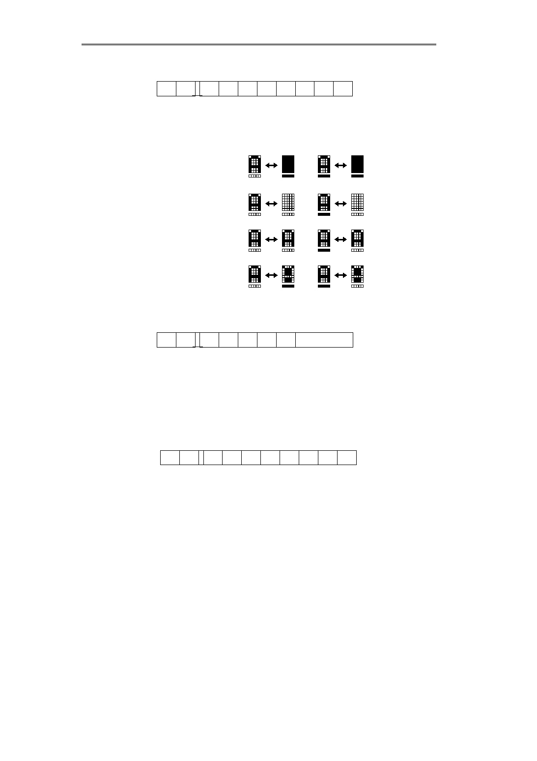
bottom of the LCD panel. When the ICON display is in no use, set the icon common output pin to
"
Open.
"
12. LCD Power Supply Circuit
Consists of a doubler, an LCD voltage controller, an LCD bias resistor, and a voltage follower. The LCD voltage controller
consists of a voltage regulator and an LCD voltage command fine adjustment circuit. The LCD power supply circuit can be
controlled by pins FNC1 and 2 and BIAS SELECT command. For power supply, an internal type for the booster, voltage
regulator and LCD voltage adjustment circuit or any external type can be switched by setting pins FNC1 or 2.
All of internal LCD power supplies will be automatically turned OFF by setting FNC1 to "H", and FNC2 to "L."
Because of this, the LCD bias voltage produced via the externally-divided resistor can be supplied to pins VLCD,
and V1 to V4.
Table 14 LCD Power Supply Circuit
FNC
1
FNC
2
Doubler
LCD Voltage
Adjustment
Circuit
LCD Bias
Resistor
Voltage
Follower
Remarks
H
H
L
L
H
L
H
L
{
×
×
×
{
×
×
×
{
×
×
{
{
×
×
{
Use all internal LCD power supply circuits.
Use an external bias resistance.
Setting is not needed.
Externally generates and inputs VLCD.
Remarks
R
Always connect FNC1 and 2 to VDD or VSS.
R
Externally-connected pins VOUT, VLCD and V1 through V4 cannot be used as a drive power supply of other
circuits.
R
Connecting the power supply externally with the internal LCD power supply circuit ON may lead to a
breakdown of the IC.
Duty
Rf
fosc
Frame Frequency
1/17 Duty
500 k
34 kHz
76.9 Hz
{
: Valid
×
: Invalid
Frame Frequency
fosc
2
×
13
×
17
[Hz]
LCD Controller-Driver
S-4561A
Seiko Instruments Inc.
15
12.1
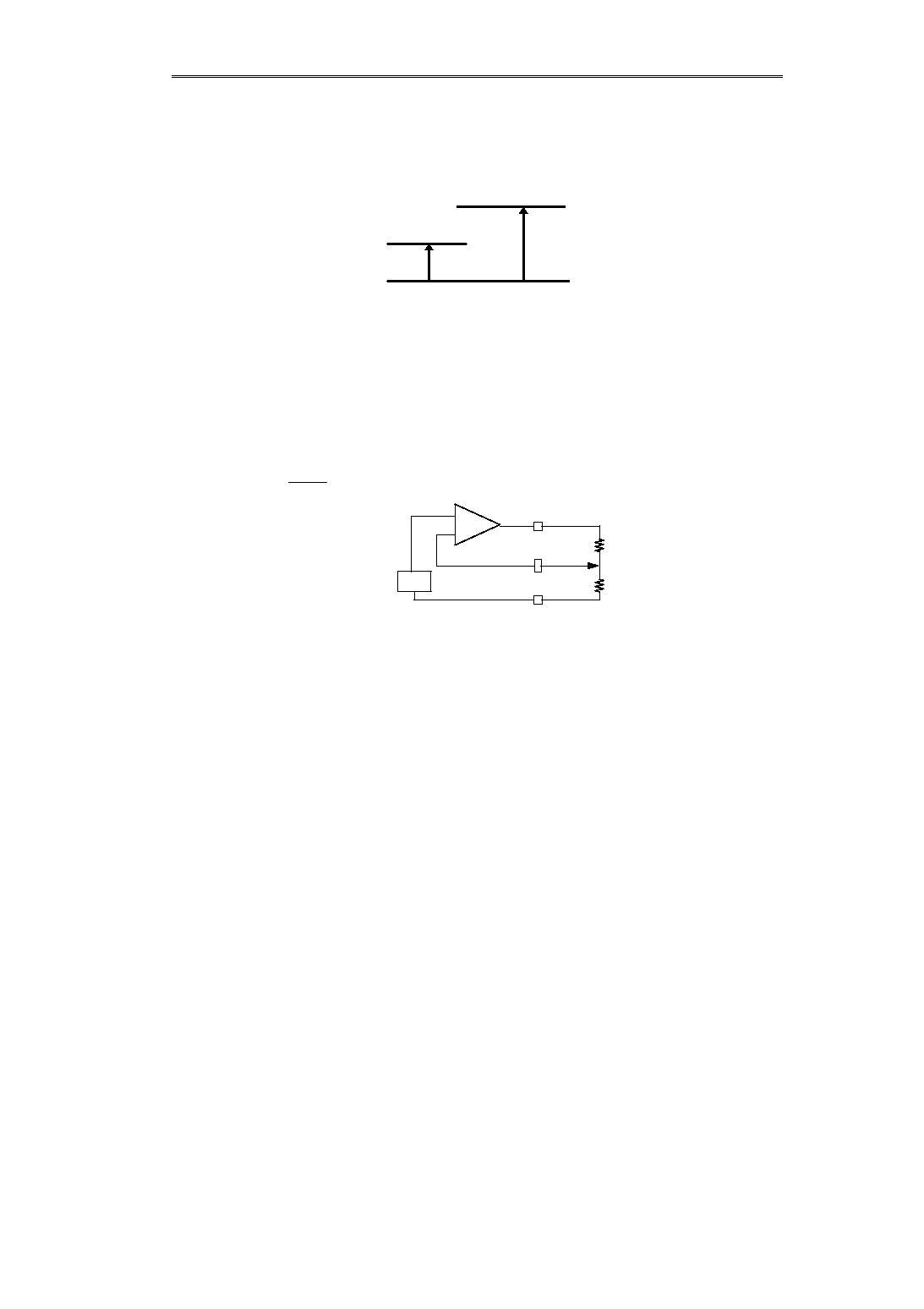
Doubler
Doubles the voltage through oscillating frequency of the CR Oscillating Circuit. The voltage is boosted from the V
SS
level and
output to V
OUT
. Capacitors between C1+ and C1- as well as between V
SS
and V
OUT
are connected. Use the doubler in the
range of V
DD
3.6 V.
12.2
LCD Voltage Adjustment Circuit
LCD drive voltage V can be adjusted by the following two voltage controllers:
R
Voltage Regulator
Adjusts voltage regulator output VLCD by externally- divided resistors Ra and Rb.
VLCD can be calculated as the division ratio of the internal reference voltage VREF. VREF has temperature
characteristics of approx. 0.01%/ C and -0.13%/ C and the LCD temperature gradient can be compensated. VREF
differs depending upon the temperature characteristics of the reference voltage to select a command.
VLCD can be used as a
"
variable
"
by using the volume resistor as the divided resistor. Feedback voltage noises
occurring at VCNT pin directly affect VLCD. Take appropriate measures against noises.
Figure 10 Example of Booster Output
V
DD
=3 V
V
SS
=0 V
Doubled Voltage VOUT=6V
Ra+Rb
V
LCD
=
Ra
V
REF
(V)
V
LCD
V
CNT
V
SS
Rb
Ra
V
REF
+
-
Figure 11 Example of LCD Voltage Adjustment Circuit

LCD Controller-Driver
S-4561A
16
Seiko Instruments Inc.
12.3
LCD Bias Resistor
The internally-divided resistor creates a bias potential for the LCD drive. Either 1/5 or 1/4 bias potential can be selected by
executing a command. Because the bias potential is supplied from bias resistor via the voltage follower to the LCD driver,
the bias current consumption is significantly reduced.
When setting FNC1 to
"
H
"
and FNC2 to
"
L,
"
the externally-attached bias resistor can be connected directly to pins V1
through V4. The bias resistor of a 1/2 or more bias ratio can be freely supplied to the LCD driver as an LCD drive voltage.
Regardless of its level, the voltage can be input to pins V1 through V4. Select an appropriate resistance value of the divided
resistor in accordance with the size and the capacity of of the LCD panel. A deflection may occur in the LCD drive waveform
depending upon the size and the capacity of the LCD panel. If so, adjust the value of the bias resistor or the capacitor.
When the external bias is selected, the bias voltage is also supplied via the voltage follower to the LCD driver. The internal
booster or the LCD voltage adjustment circuit cannot be used.
Supply VLCD via the externally-attached LCD power supply circuit.
12.4
Voltage Follower
Buffers the bias potential via the internal bias resistor and supplies it to the LCD driver.
12.5
Reference Voltage Circuit
Generates reference voltage VREF. The VREF has the following three values:
Table 15 V
REF
V
REF
DV1
DV0
Temperature
Characteristics
Reference
Voltage
0
0
1
0
1
*
-0.13%/
°
C
0.01%/
°
C
1.7 V (Standard)
1.7 V (Standard)
V
DD
LCD Controller-Driver
S-4561A
Seiko Instruments Inc.
17
s
Instruction Explanation
The instruction comes in two types - - namely, normal instructions and extended instructions. All instructions excluding the
DISPLAY CLEAR are completed within the instruction command cycle time. Because of this, the CPU does not need for
checking the BUSY flag, and instructions can be input in succession.
1. Normal Instructions
1.1 DISPLAY CLEAR
Clears the display and initializes the state. The display of marks remains unchanged.
DDRAM
: Writes 20H in hexadecimal scale.
DDRAM Address Counter
: Sets address 0. Clears the DISPLAY SHIFT and returns to the default.
Entry Mode
: Sets to ID=1 [increment].
"
S
"
remains unchanged.
Cursor
: The CURSOR DISPLAY position moves to the 1st line, left end.
"
C
"
remains
unchanged.
Blink
: The BLINK DISPLAY position moves to the 1st line, left end.
"
B
"
remains
unchanged.
Amount of smooth scroll
: Resets the amount of scroll.
The DISPLAY CLEAR needs the time for writing space codes in succession in all of DDRAMs. Confirm the completion of the
DISPLAY CLEAR command by checking the BUSY flag. When you wait for the time expressed by equation (1) after
executing the DISPLAY CLEAR command, the BUSY flag does not need to be checked (the value twice as many as the
value expressed in equation (1) is recommended as the wait time).
The contents of the CGRAM, ICONRAM, and ICON BLINK RAM remain unchanged.
The DISPLAY CLEAR command is ignored during the POWER SAVE.
Remark: Always set all space codes in
"
20
"
(hexadecimal scale).
1.2 CURSOR HOME
Initializes the cursor position and the blink position. The contents of the CHARACTER DISPLAY and the ICON DISPLAY
remain unchanged. After this instruction is executed, data is read from the CPU and written in the DDRAM.
z
CH=1 (Cursor Home)
DDRAM Address Counter
: Sets the address to 0.
DISPLAY SHIFT
: Clears the amount of the DISPLAY SHIFT and returns to the initial display screen.
CURSOR
: The CURSOR DISPLAY position moves to the 1st line, left end.
"
C
"
remains
unchanged.
BLINK
: The BLINK DISPLAY position moves to the 1st line, left end.
"
B
"
remains unchanged.
Amount of SMOOTH SCROLL : Resets the amount of the SCROLL and returns to the initial display screen.
z
CH=0 (Cursor Return)
DDRAM Address Counter
: Sets the 1st address on the CURSOR DISPLAY line.
DISPLAY SHIFT
: Clears the amount of the DISPLAY SHIFT and returns to the initial display screen.
CURSOR
: The CURSOR DISPLAY position moves to the same line, left end.
"
C
"
remains
unchanged.
BLINK
: The BLINK DISPLAY position moves to the 1st line, left end.
"
B
"
remains unchanged.
Amount of SMOOTH SCROLL : Resets the amount of the SCROLL and returns to the initial display screen.
RS
0
R/WX
0
DB7
0
DB6
0
DB5
0
DB4
0
DB3
0
DB2
0
DB1
0
DB0
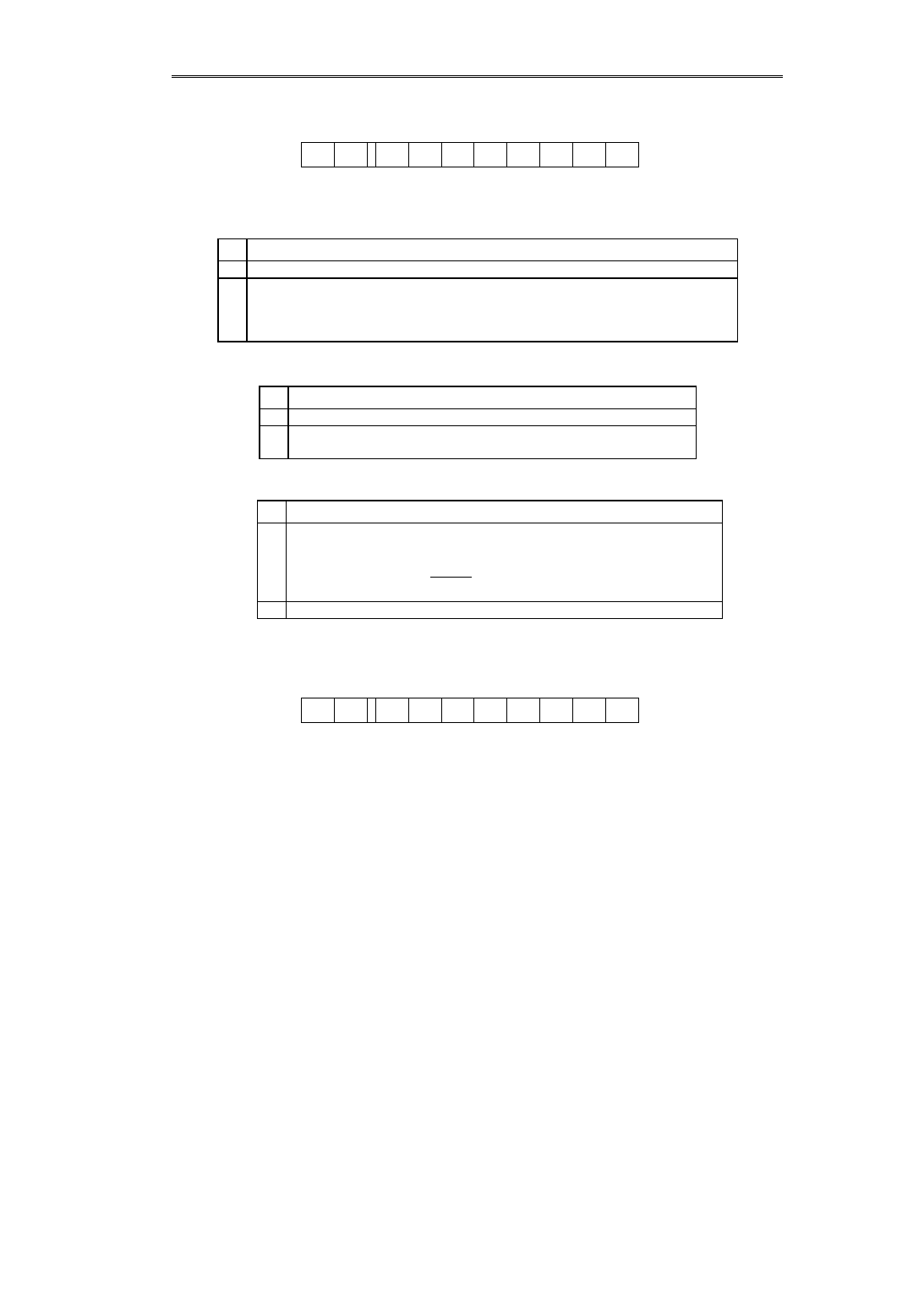
1
Normal
Time until DISPLAY CLEAR is completed=
35
fosc(kHz)
msec
Equation (1)
RS
0
R/WX
0
DB7
0
DB6
0
DB5
0
DB4
0
DB3
0
DB2
0
DB1
1
DB0
CH
Normal
LCD Controller-Driver
S-4561A
18
Seiko Instruments Inc.
1.3 ENTRY MODE SETTING
When data is written in and read from the DDRAM, CGRAM, ICONRAM, or the ICON BLINK RAM in accordance with the ID,
set ID=1 [increment] or ID=0 [decrement] of the selected RAM address counter.
"
S
"
determines whether or not the whole display shifts during the write in the DDRAM. The display shifts left when ID=1,
and shifts right when ID=0.
Table 16 Operations of Address Counter
ID
Access from/to
RAM
Operations of Address Counter
0
DDRAM
CGRAM: After write
ICONRAM: After read
ICON BLINK RAM
R
Decrements the address counter of the RAM (-1)
after executing write and read.
1
DDRAM
CGRAM: After write
ICONRAM: After read
ICON BLINK RAM
R
Increments the address counter of the RAM (+1)
after executing write and read.
Notes:
--
:
Don't care.
*
:
The display shifts. CURSOR and BLINK positions seem to be standstill on the display screen.
CURSOR and BLINK displays are valid only when
"
1
"
is set to DISPLAY ON/OFF command C or B.
Access from/to
RAM
ID
S
Display Shift
1
1
R
Shifts the whole display left.
R
CURSOR and BLINK positions remain unchanged.*
Write in DDRAM
0
R
The display does not shift.
R
CURSOR and BLINK positions shift right.
0
1
R
Shifts the whole display right.
R
CURSOR and BLINK positions remain unchanged.
0
R
The display does not shift.
R
CURSOR and BLINK positions shift left.
Read from DDRAM
1
-
R
The display does not shift.
R
CURSOR and BLINK positions shift right.
0
-
R
The display does not shift.
R
CURSOR and BLINK positions shift left.
CGRAM
Write in ICONRAM
Read from ICON BLINK
RAM
-
-
R
The display does not shift.
R
CURSOR and BLINK positions do not shift.
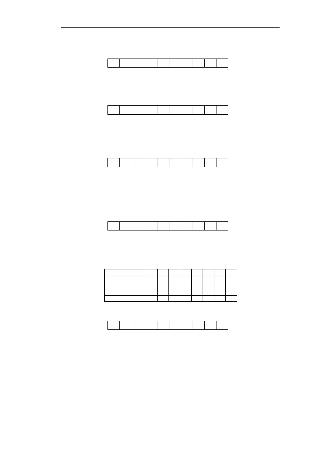
RS
0
R/WX
0
DB7
0
DB6
0
DB5
0
DB4
0
DB3
0
DB2
1
DB1
ID
DB0
S
Normal
Table 17 Display Shift
LCD Controller-Driver
S-4561A
Seiko Instruments Inc.
19
1.4 DISPLAY ON/OFF
"
D
"
,
"
C
"
and
"
B
"
set the DISPLAY ON/OFF, CURSOR DISPLAY ON/OFF and BLINK DISPLAY ON/OFF.
Table 18 D
D
Functions
1
Turns ON the display (display start).
0
R
Turns OFF the CHARACTER DISPLAY, MARK DISPLAY, CURSOR DISPLAY, and BLINK DISPLAY.
R
Data of the DDRAM, CGRAM, ICONRAM, and ICON BLINK RAM remain unchanged.
R
Displays again when turning ON the display.
Remark:
There is no change in the current consumption when turning OFF the display.
Table 19 C
C
Functions
1
Displays the cursor at the position of the DDRAM address counter.
0
Turns OFF the CURSOR DISPLAY.
There is no change in setting values such as ID.
Table 20 B
1.5 CURSOR/DISPLAY SHIFT
Shifts CURSOR and BLINK positions without writing in and reading from the display data. Used for character correction and
retrieval.
Data is written in and read from the CPU to the DDRAM after executing this command.
B
Functions
1
Continues blinking the characters at the position of the DDRAM address counter.
Can set the CURSOR and BLINK at the same time.
0
Aborts the blink.
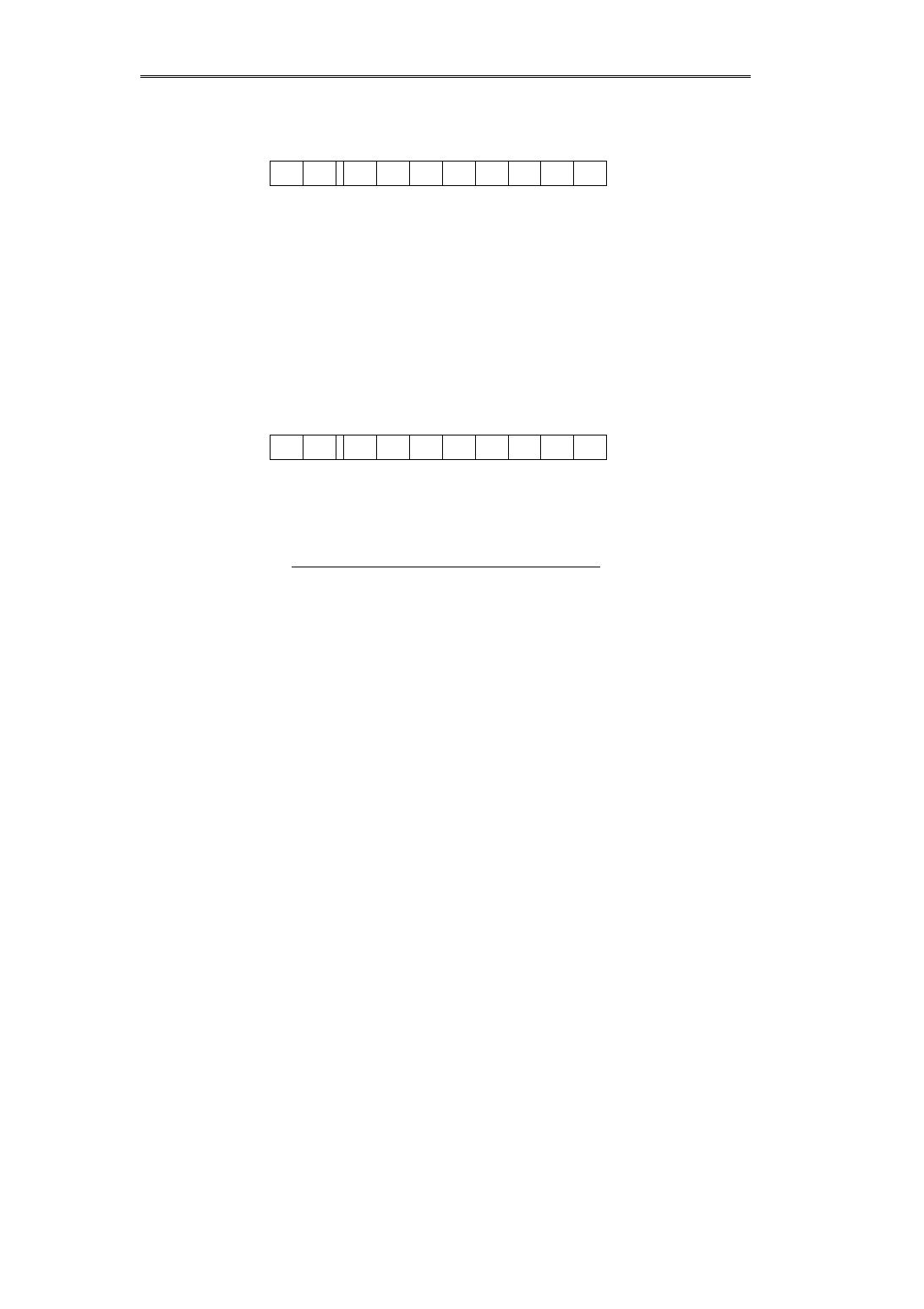
RS
0
R/WX
0
DB7
0
DB6
0
DB5
0
DB4
0
DB3
1
DB2
D
DB1
C
DB0
B
Normal
Blink Frequency=
32768
[Hz]
fosc
RS
0
R/WX
0
DB7
0
DB6
0
DB5
0
DB4
1
DB3
SC
DB2
RL
DB1
-
DB0
-
Normal
- : Don't care
LCD Controller-Driver
S-4561A
20
Seiko Instruments Inc.
Table 21 Cursor/Display Shift
SC
RL
Functions
0
0
Shifts CURSOR and BLINK positions left.
Decrements the DDRAM address counter (-1).
Repetitious operations of the CURSOR SHIFT move the cursor to other line.
0
1
Shifts CURSOR and BLINK positions right.
Increments the DDRAM address counter (+1).
Repetitious operations of the CURSOR SHIFT move the cursor to other line.
1
0
Shifts the whole display left.
Shifts CURSOR and BLINK positions left, together with characters.
There is no change in the DDRAM address counter.
Characters do not shift to other line even when the DISPLAY SHIFT is executed in succession.
1
1
Shifts the whole display right.
Shifts CURSOR and BLINK positions right, together with characters.
There is no change in the DDRAM address counter.
Characters do not shift to other line even when the DISPLAY SHIFT is executed in succession.
1.6 FUNCTION SET
1.6.1
DL
Sets the length of data for parallel interface.
0 :
4-bit data length interface
1 :
8-bit data length interface
1.6.2
N
Sets the display screen.
N : 0
Selects a 2-line x 12 column display.
N : 1
Selects a 1-line x 24 column display.
1.6.3
MS
Selects the instruction table.
Table 22 MS
MS
Functions
0
Selects the Normal Instruction Table.
Sets
"
0
"
when changing from the Extended Instruction Table.
1
Selects the Extended Instruction Table.
Sets
"
1
"
when changing from the Normal Instruction Table.
1.6.4
DT
Table 22 DT
DT
Functions
0
5-dot display mode
1
6-dot display mode
RS
0
R/WX
0
DB7
0
DB6
0
DB5
1
DB4
DL
DB3
N
DB2
MS
DB1
DT
DB0
-
Normal
LCD Controller-Driver
S-4561A
Seiko Instruments Inc.
21
1.7 CGRAM ADDRESS SETTING
Sets binary
"
A5A4A3A2A1A0
"
to the CGRAM Address Counter.
After executing this command, data is written from the CPU and read in the CGRAM.
1.8 DDRAM ADDRESS SETTING
Sets binary
"
A4A3A2A1A0
"
to the DDRAM Address Counter.
After executing this command, data is written from the CPU and read in the DDRAM.
1.9 BUSY FLAG/ADDRESS READ
Reads the BUSY flag and the content of
"
A5A4A3A2A1A0
"
of the Address Counter. Outputs BUSY flag BF
"
1
"
to DB7 during
execution of a command. Execution of any command excluding the DISPLAY CLEAR is completed within the command
cycle time. Therefore, confirmation of the BUSY flag is not needed.
The Read Address Counter reads the contents of the RAM address counter accessed just before executing this command
among DDRAM, CGRAM, ICONRAM, and ICON BLINK RAM.
1.10
DATA WRITE
Writes binary data
"
D7D6D5D4D3D2D1D0
"
in CGRAM, DDRAM, ICONRAM, and ICON BLINK RAM. Prior to data write,
execute the desired RAM ADDRESS SETTING command to select an appropriate RAM. Addresses after write are
incremented or decremented depending upon the ID value in the entry mode.
Table 24 Length of Data of Each Memory
DB7
DB6
DB5
DB4
DB3
DB2
DB1
DB0
DDRAM
D
7
D
6
D
5
D
4
D
3
D
2
D
1
D
0
CGRAM
*
*
*
D
4
D
3
D
2
D
1
D
0
ICONRAM
*
*
*
D
4
D
3
D
2
D
1
D
0
ICON BLINK RAM
*
*
*
D
4
D
3
D
2
D
1
D
0
1.11
DATA READ
Reads binary
"
D7D6D5D4D3D2D1D0
"
from CGRAM, DDRAM, ICONRAM, ICON BLINK RAM. Prior to data write, execute
the desired RAM ADDRESS SETTING command to select an appropriate RAM. Addresses after write are incremented or
decremented depending upon the ID value in the entry mode.
RS
0
R/WX
0
DB7
0
DB6
1
DB5
A
5
DB4
A
4
DB3
A
3
DB2
A
2
DB1
A
1
DB0
A
0
Normal
RS
0
R/WX
0
DB7
1
DB6
-
DB5
-
DB4
A
4
DB3
A
3
DB2
A
2
DB1
A
1
DB0
A
0
Normal
- : Don't care
RS
0
R/WX
1
DB7
BF
DB6
0
DB5
A
5
DB4
A
4
DB3
A
3
DB2
A
2
DB1
A
1
DB0
A
0
Normal
RS
1
R/WX
0
DB7
D
7
DB6
D
6
DB5
D
5
DB4
D
4
DB3
D
3
DB2
D
2
DB1
D
1
DB0
D
0
Normal
RS
1
R/WX
1
DB7
D
7
DB6
D
6
DB5
D
5
DB4
D
4
DB3
D
3
DB2
D
2
DB1
D
1
DB0
D
0
Normal
LCD Controller-Driver
S-4561A
22
Seiko Instruments Inc.
2. Extended Instructions
2.1 POWER SAVE SETTING
PS
: 1 Power Save
R
Aborts the oscillating circuit and the LCD power supply circuit.
R
Aborts the LCD driver. Segment, and common LCD drive outputs are fixed to VSS.
R
Aborts the LCD.
R
Leaves the setting of individual data, common and address in the DDRAM, CGRAM, ICONRAM, ICON BLINK
RAM unchanged.
PS
: 0 Cancels Power Save
In the Power Save mode, the current consumption is minimized to approximate the value during standstill.
When the external power supply is used, it is necessary to stop it and go to the floating or the VSS level. Also, a switching
transistor and other circuit which cut the current flowing through the external bias resistor are needed.
2.2 SELECTING ICON ONLY DISPLAY, BOOSTER DRIVE FREQUENCY
MD : 0
Normal Display
MD : 1
Icon Only Display
DC
: Booster Drive Frequency Setting
DC1
DC0
Booster Drive Frequency [kHz]
1/17 Duty fosc=34 kHz
0
0
1
1
0
1
0
1
Default
4.25 (1/8 osc)
2.13 (1/16 osc)
1.06 (1/32 osc)
0.53 (1/64 osc)
Regardless of the contents of the DDRAM, the icon only is displayed and display screens excluding marks go out when
MD=1. When setting the booster drive frequency, it is possible to minimize the current consumption by reducing the booster
drive frequency in accordance with the boosting control data.
When the booster drive frequency is reduced, the contrast of the display icon differs depending upon the display panel size
and the value of the capacitor for the booster. Determine the ability of the booster by experimentally optimizing the contrast
of the LCD panel. In addition, take into careful consideration noises which may affect the system due to the booster drive
frequency.
After resetting, the booster drive frequency is the default value.
RS
0
R/WX
0
DB7
0
DB6
0
DB5
0
DB4
0
DB3
-
DB2
-
DB1
-
DB0
PS
Extended
- : Don't care
RS
0
R/WX
0
DB7
0
DB6
0
DB5
0
DB4
1
DB3
-
DB2
MD
DB1
DC1
DB0
DC0
Extended
- : Don't care
LCD Controller-Driver
S-4561A
Seiko Instruments Inc.
23
2.3 SELECT COM/SEG OUTPUT MODE, SELECT BIAS
The MLC determines how the common output waveform is output to COM (1-16) terminals.
MLC=0:
The common output waveform is output in the order of COM1, COM2,
NNN
, COM15, COM16.
MLC=1:
The common output waveform is output in the order of COM16, COM15,
NNN
, COM2, COM1.
The MLS determines how the segment output waveform is output to SEG (1-60) terminals.
The output form also varies depending upon N=0 or N=1.
[N=0 (2-line x 12-column) display]
MLS=0:
The segment output waveform to be displayed on the DDRAM addresses from 00 to 0B is output to
terminals from SEG1 to SEG60.
The segment output waveform to be displayed on the DDRAM addresses from 10 to 1B is output to
terminals from SEG1 to SEG60.
MLS=1:
The segment output waveform to be displayed on the DDRAM addresses from 00 to 0B is output to
terminals from SEG60 to SEG1.
The segment output waveform to be displayed on the DDRAM addresses from 10 to 1B is output to
terminals from SEG60 to SEG1.
[N=1 (1-line x 24-column) display]
MLS=0:
The segment output waveform to be displayed on the DDRAM addresses from 00 to 0B is output to
terminals from SEG1 to SEG60.
The segment output waveform to be displayed on the DDRAM addresses from 10 to 1B is output to
terminals from SEG60 to SEG1.
MLS=1:
The segment output waveform to be displayed on the DDRAM addresses from 00 to 0B is output to
terminals from SEG60 to SEG1.
The segment output waveform to be displayed on the DDRAM addresses from 10 to 1B is output to
terminals from SEG1 to SEG60.
Both the MLC and the MLS allow viewers to see characters correctly regardless of the mounting position of the IC to the LCD
panel (upper, lower, front or rear mounting position).
Determine the bias voltage for the LCD power supply circuit.
BS5
Select Bias
0
1/4 Bias
1
1/5 Bias
While the bias voltage is being externally determined, the booster, the LCD voltage adjustment circuit, the voltage follower,
and the bias circuit stop.
RS
0
R/WX
0
DB7
0
DB6
1
DB5
0
DB4
0
DB3
MLC
DB2
MLS
DB1
DB0
BS5
Extended
LCD Controller-Driver
S-4561A
24
Seiko Instruments Inc.
2.4 BLINK SELECT
Four kinds of blink display are set up.
2.5 SMOOTH SCROLL DOT SHIFT AMOUNT SETTING
Set the dot scroll amount of the selected line to the smooth scroll line and shift it. The display shifts left by the dot scroll
amount. The dot scroll amount is from 0 dot up to 5 dots. The dot scroll amount of over 6 dots is deemed to be 0 dot. To
continue smooth scroll, execute the SMOOTH SCROLL CHARACTER command. The scroll amount can be reset by
executing the SMOOTH SCROLL CHARACTER SHIFT, DISPLAY CLEAR or CURSOR HOME command.
The smooth scroll amount is cleared by resetting the smooth scroll amount character shift amount.
2.6 SETTING UP SMOOTH SCROLL LINE
Set the smooth scroll line. The line where
"
1
"
is set on L1, L2 is selected. To scroll two lines simultaneously, set
"
1
"
to L1
and L2.
L2:
2nd line
L1:
1st line
To scroll another line while a line is being scrolled, release the smooth scroll character amount and line setup, then set a new
scroll line.
BK1
BK0
Cursor Display OFF
C=0
Cursor Display ON
C=1
Black Blink
0
0
B=0
B=0
White Blink
0
1
Cursor Blink
1
0
White/Black
Inversion Blink
1
1
RS
0
R/WX
0
DB7
0
DB6
1
DB5
0
DB4
1
DB3
-
DB2
-
DB1
BK1
DB0
BK0
Extended
- : Don't care
RS
0
R/WX
0
DB7
1
DB6
0
DB5
0
DB4
0
DB3
-
DB2
-
DB1
BK1
DB0
BK0
Extended
Scroll Amount
RS
0
R/WX
0
DB7
1
DB6
0
DB5
0
DB4
1
DB3
-
DB2
-
DB1
L
2
DB0
L
1
Extended
- : Don't care
LCD Controller-Driver
S-4561A
Seiko Instruments Inc.
25
2.7 SMOOTH SCROLL CHARACTER SHIFT AMOUNT SETTING
Shift the required number of characters of the selected line to the smooth scroll line.
S4
S3
S2
S1
S0
Shift Amount
0
0
0
0
0
Does not shift.
0
0
0
0
1
1 character shifts left.
0
0
0
1
0
2 characters shift left.
:
:
1
0
0
0
0
16 characters shift left.
:
:
1
1
1
1
1
31 characters shift left.
2.8 ICONRAM ADDRESS SETTING
Set binary
"
A3A2A1A0
"
to the ICONRAM Address Counter.
After this command is executed, data is written from the CPU and read to ICONRAM. Write the mark display data which
corresponds to each address of the ICONRAM for every 5 bits.
2.9 ICON BLINK RAM ADDRESS SETTING
Set binary
"
A3A2A1A0
"
to the ICON BLINK RAM Address Counter. When writing
"
1
"
in the ICON BLINK RAM, the
respective marks blink. ICONRAM addresses correspond to respective ICON BLINK RAM addresses. After this command is
executed, data is written from the CPU and read to ICON BLINK RAM.
2.10 (TEST)
Testbits:D
3
D
0
= all 0 at reset.
DO NOT write any values other than
"
0000
"
into this testbits.
RS
0
R/WX
0
DB7
1
DB6
0
DB5
1
DB4
S
4
DB3
S
3
DB2
S
2
DB1
S
1
DB0
S
0
Extended
RS
0
R/WX
0
DB7
1
DB6
1
DB5
0
DB4
0
DB3
A
3
DB2
A
2
DB1
A
1
DB0
A
0
Extended
RS
0
R/WX
0
DB7
1
DB6
1
DB5
0
DB4
1
DB3
A
3
DB2
A
2
DB1
A
1
DB0
A
0
Extended
RS
0
R/WX
0
DB7
1
DB6
1
DB5
1
DB4
0
DB3
D
3
DB2
D
2
DB1
D
1
DB0
D
0
Extended
LCD Controller-Driver
S-4561A
26
Seiko Instruments Inc.
2.11 REFERENCE VOLTAGE CHARACTERISTICS SELECT
Select the temperature characteristics for the reference voltage. The reference voltage also varies depending upon the
temperature characteristics.
DV1
DV0
Temperature Characteristics(%/
°
C)
V
REF
Reference Voltage(Ta=25
°
C)
V
REF
(V)
0
0
1
0
1
0.13
0.01
0
1.7
1.7
VDD
2.12 FUNCTION SETTING
The same as the function setting for the Normal Instructions.
2.13 BUSY FLAG/ADDRESS READ
The same as the functions for the Normal Instructions.
2.14 DATA WRITE
The same as the functions for the Normal Instructions.
2.15 DATA READ
The same as the functions for the Normal Instructions.
RS
0
R/WX
0
DB7
1
DB6
1
DB5
1
DB4
1
DB3
-
DB2
-
DB1
DV1
DB0
DV0
Extended
RS
0
R/WX
0
DB7
0
DB6
0
DB5
1
DB4
DL
DB3
N
DB2
MS
DB1
DT
DB0
-
Extended
RS
0
R/WX
1
DB7
BF
DB6
0
DB5
A
5
DB4
A
4
DB3
A
3
DB2
A
2
DB1
A
1
DB0
A
0
Extended
RS
1
R/WX
0
DB7
D
7
DB6
D
6
DB5
D
5
DB4
D
4
DB3
D
3
DB2
D
2
DB1
D
1
DB0
D
0
Extended
RS
1
R/WX
1
DB7
D
7
DB6
D
6
DB5
D
5
DB4
D
4
DB3
D
3
DB2
D
2
DB1
D
1
DB0
D
0
Extended
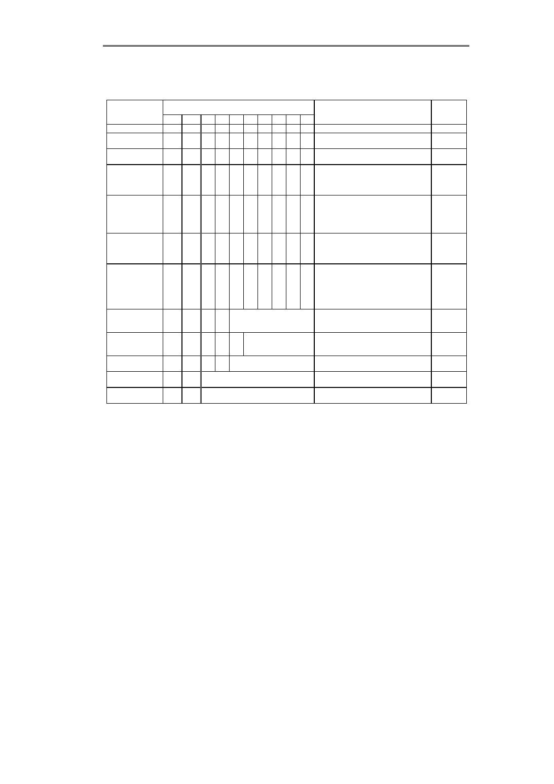
LCD Controller-Driver
S-4561A
Seiko Instruments Inc.
27
s
Instruction List
1.
Normal Instructions
Table 25 Normal Instructions
-:Don't care
Command
Code
Description
Execution
Time
RS
R/WX DB7 DB6 DB5 DB4 DB3 DB2 DB1 DB0
V
DD
=3V
NOP
0
0
0
0
0
0
0
0
0
0
Don
'
t care.
DISPLAY CLEAR
0
0
0
0
0
0
0
0
0
1
Writes the space code in the entire
DDRAM.
OSC 35
Clock
CURSOR HOME
0
0
0
0
0
0
0
0
1
CH
CH: 1/0= Cursor Return/Cursor Home
1
µ
sec
or less
ENTRY MODE
0
0
0
0
0
0
0
1
ID
S
ID:
1/0=
Address Counter
Increment/Decrement
S:
1/0=
Display Shift during
DDRAM write
1
µ
sec
or less
DISPLAY ON/OFF
0
0
0
0
0
0
1
D
C
B
D:
1/0=
Display ON/OFF
C:
1/0=
Cursor Display
ON/OFF
B:
1/0=
Cursor Position Blink
ON/OFF
1
µ
sec
or less
CURSOR
DISPLAY SHIFT
0
0
0
0
0
1
SC
RL
-
-
SC:
1/0=
Whole Display
Shift/Cursor Shift
RL:
1/0=
Cursor/Display Right
/Left Shift
1
µ
sec
or less
FUNCTION
SETTING
0
0
0
0
1
DL
N
MS DT
-
DL: 1/0=
8-bit/4-bit Data Length
Interface
N: 1/0=
1-line x 24-column/2-line x
12- column
MS: 1/0= Extended/Normal Interface
DT: 1/0=
6-dot front/5-dot font
1
µ
sec
or less
CGRAM
ADDRESS
SETTING
0
0
0
1
CGRAM Address
CGRAM Address Setting
1
µ
sec
or less
DDRAM
ADDRESS
SETTING
0
0
1
-
-
DDRAM Address
DDRAM Address Setting
1
µ
sec
or less
BUSY
ADDRESS READ
0
1
BF
0
Address Counter
BF:
BUSY Output
Address Counter Read
1
µ
sec
or less
DATA WRITE
1
0
Write Data
Write Data
1
µ
sec
or less
DATA READ
1
1
Address Counter
Data Read
1
µ
sec
or less
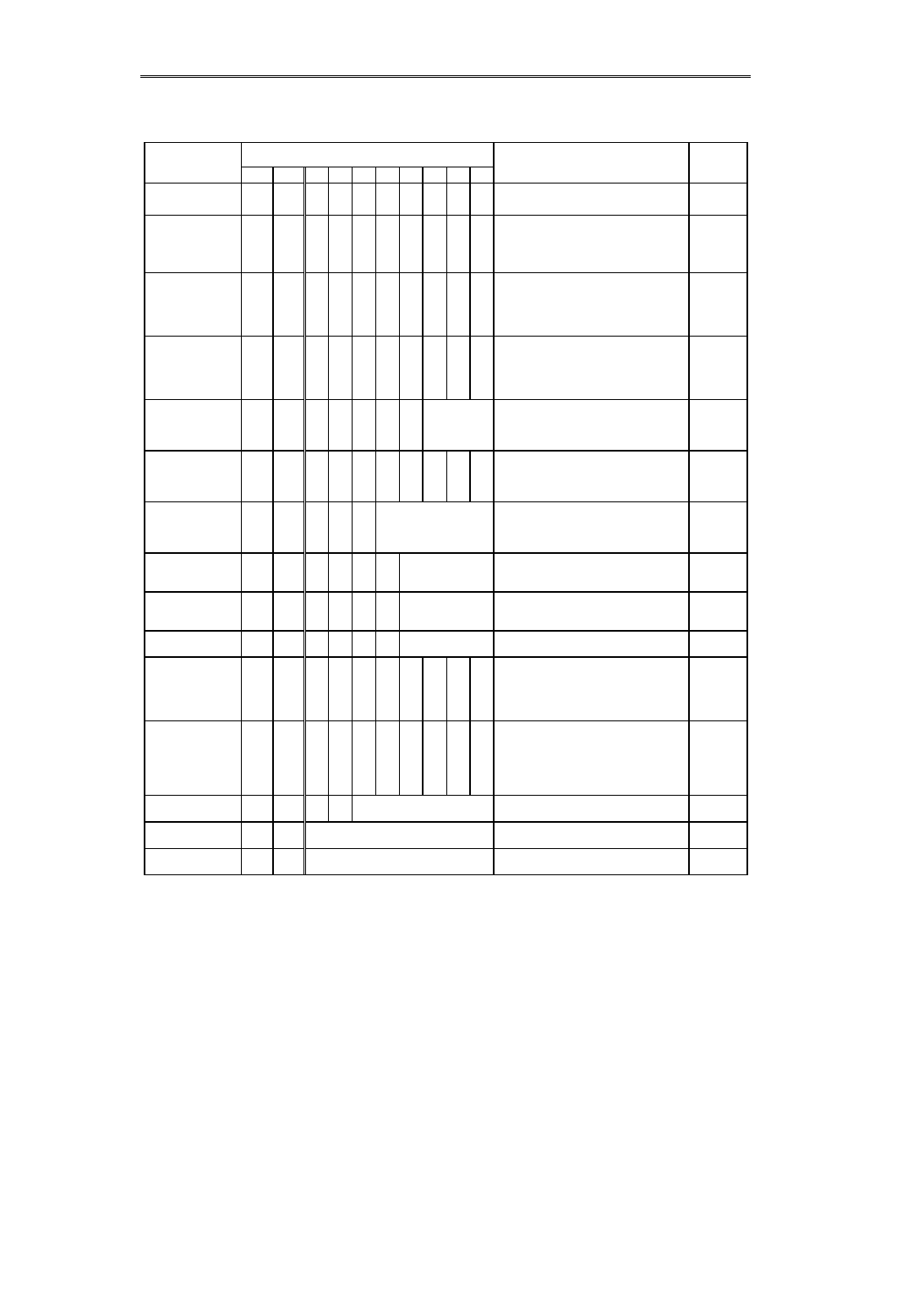
LCD Controller-Driver
S-4561A
28
Seiko Instruments Inc.
2.
Extended Instructions
Table 26 Extended Instructions
IMPORTANT:
The FUNCTION SETTING, BUSY ADDRESS READ, DATA WRITE, and DATA READ commands are
common to Normal and Extended Instructions.
** This is for Biastest. Testbits=
"
all0
"
at reset. DO NOT write any values other than
"
0000
"
into this testbits.
Command
Code
Description
Execution
Time
RS
R/WX DB7 DB6 DB5 DB4 DB3 DB2 DB1 DB0
V
DD
=3V
POWER SAVE
SETTING
0
0
0
0
0
0
0
0
0
PS PS : 1/0=
Power Save
Operation/Normal Display
1
µ
sec
or less
ICON ONLY
DISPLAY
BOOSTER DRIVE
FREQUENCY
0
0
0
0
0
1
-
MD DC1 DC0
MD : 1/0= Icon Only Display/Normal
Entire Display
DC1, DC0: Booster Drive Frequency
Select
1
µ
sec
or less
COM/SEG
OUTPUT MODE
SELECT
BIAS SELECT
0
0
0
1
0
0
MLC MLS
-
BS5
MLC:
COM Output Mode
MLS:
SEG Output Mode
BS5:
1 (1/5 Bias)
0
(1/4 Bias)
1
µ
sec
or less
BLINK SELECT
0
0
0
1
0
1
-
-
BK1 BK0
BK1BK0
0
0
Black Blink
0
1
White Blink
1
0
Cursor Blink
1
1
Black/White Inverse Blink
1
µ
sec
or less
SMOOTH SCROLL
DOT SHIFT
0
0
1
0
0
0
-
Dot
Shift Amount
Dot Shift Amount :
Sets and executes the Dot Shift
Amount in the Smooth Scroll Select
lines.
1
µ
sec
or less
SCROLL LINE
SETTING
0
0
1
0
0
1
-
-
L2
L1
L1: Selects the 1st line to Smooth
Scroll line.
L2: Select the 2nd line to the Smooth
Scroll line.
1
µ
sec
or less
SMOOTH SCROLL
CHARACTER
SHIFT
0
0
1
0
1
Character
Shift Amount
Character Shift Amount:
Setting and Operation of the
Character Shift Amount in the
Smooth Scroll Select lines.
1
µ
sec
or less
ICON RAM
ADDRESS
SETTING
0
0
1
1
0
0
Icon RAM Address Icon RAM Address Assignment
1
µ
sec
or less
ICON BLINK RAM
ADDRESS
SETTING
0
0
1
1
0
1
Icon Blink
RAM Address
Icon Blink RAM Address Assignment/
Sets the Icon to blink.
1
µ
sec
or less
** (TEST)
0
0
1
1
1
0
Testbits
**
1
µ
sec
or less
REFERENCE
VOLTAGE
CHARACTERISTI-
CS SELECT
0
0
1
1
1
1
-
-
DV1 DV0
DV1 DV0 Characteristics Reference V
0
0
-0.13%/
°
C
1.7 V
0
1
0.01%/
°
C
1.7 V
1
VDD
1
µ
sec
or less
FUNCTION
SETTING
0
0
0
0
1
DL
N
MS DT
-
DL:1/0= 8-bit/4-bit data Length Interface
N:1/0=
1-line x 24-column/2-line x 12-
column
MS:
1/0= Extended/Normal
Instructions
DT:
1/0= 6-dot/5-dot font
1
µ
sec
or less
BUSY
ADDRESS READ
0
1
BF
0
Address Counter
BF : BUSY Output
Address Counter Read
1
µ
sec
or less
DATA WRITE
1
0
Write Data
Write Data
1
µ
sec
or less
DATA READ
1
1
Read Data
Read Data
1
µ
sec
or less

LCD Controller-Driver
S-4561A
Seiko Instruments Inc.
29
s
Operation Description
1.
Powering ON
After powering ON, the S-4561A is initialized by inputting the RESX signal.
In order to prevent the unstable state of the inside of the IC due to momentary stop or gradually raised power voltage
waveform, reset hardware by inputting the RESX signal.
If the S-4561A is not initialized by inputting the RESX signal, the IC may malfunction. Chattering occurring in the RESX
signal may lead to an initialization error. Input the signal free of chattering. Always connect and fix pins P/SX, FNC1 and
FNC2 to V
DD
or V
SS
.
2.
Reset
The following operations and instructions are executed by initialization through the RESX signal input:
1
Entire Circuitry Reset
2
Bias Select
BS5=1 (1/5 Bias)
3
Display OFF
D=0, C=0, B=0
4
Display Clear
q
DDRAM Address
Reset
"
00000
"
q
Smooth Scroll Dot shift Amount
Reset
"
000
"
q
Smooth scroll line
Reset
"
0000
"
q
Smooth Scroll Dot Shift Amount
Reset
"
00000
"
5
Entry Mode
ID=1, S=0
6
Icon Only Display
OFF (MD=0)
q
Booster Drive Frequency
01
7
Blink mode
Black blink
"
00
"
8
ICONRAM Address
Reset
"
0000
"
9
ICON BLINK RAM Address
Reset
"
0000
"
10 (TEST)
Reset
"
0000
"
11 Function Setting
Set to the normal instruction set
DL=1, N=0, MS=0, DT=0
12 Address Counter
Select DDRAM
13 Reference Voltage Temperature Characteristics Select
00 (- 0.13%/
°
C)
14 Power Save
After resetting, the state moves to PS=1.
q
Booster
OFF
q
LCD power Supply Voltage Controller
OFF
q
Voltage Regulator
OFF
q
Bias Resistor
OFF
Remark: After resetting, the state automatically moves to the Power Save mode
.
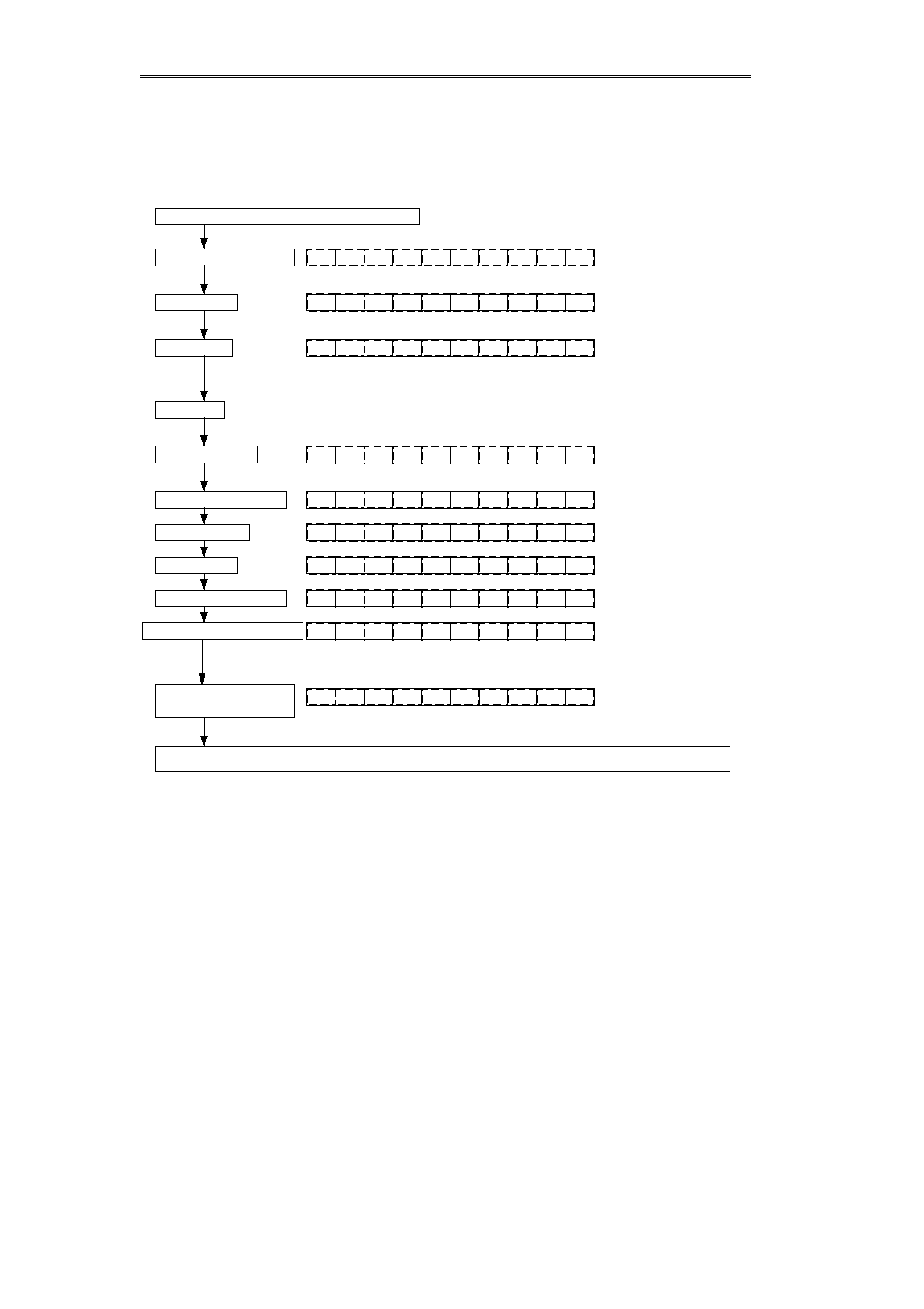
LCD Controller-Driver
S-4561A
30
Seiko Instruments Inc.
3.
Initialization by Instruction
When initializing the IC by instruction, input the necessary command and set to the appropriate mode, referring to the
following order.
After powering ON, reset the state by inputting the RESX signal, instead of initializing the IC by the instruction.
1
0
0
-
Example of Initialization Using the Instruction
Normal Function Setting
Display ON/OFF
Display Clear
0
Referential Setting
q
8-bit data length interface
q
2-line x 12-column
q
5-dot font
q
Display OFF
q
Cursor Display OFF
q
Blink OFF
RS
0
R/WX
0
DB7
0
DB6
1
DB5
1
DB4
0
DB3
0
DB2
0
DB1
-
DB0
0
0
0
0
0
0
1
0
0
0
0
0
0
0
0
0
0
0
0
1
q
DDRAM Clear
q
DDRAM Address Counter Reset
q
Cursor Home
q
Smooth Scroll Reset
q
ID=1 Increment Setting
1.03 msec when fosc=34 kHz
Wait Time
Entry Mode Setting
q
ID=1 Increment
S=0
No Display Shift
0
0
0
0
0
0
0
1
1
Extended Function Setting
0
0
0
0
1
1
0
1
0
-
Icon Only Display
0
0
0
0
0
1
-
0
1
1
q
Normal Display
q
Booster Drive Frequency
"
11
"
BLINK Select
0
0
0
1
0
1
-
-
0
0
q
Black/White Blink
ICONRAM Address Setting
0
0
1
1
0
0
0
0
0
0
q
ICONRAM Address
Reset
"
0000
"
ICON Blink RAM Address Setting
0
0
1
1
0
1
0
0
0
0
q
ICON BLINK RAM Address
Reset
"
0000
"
Write in the specified instruction set, CGRAM, DDRAM, and ICONRAM. Display ON and other commands.
0
Reference Voltage vs
Temperature Characteristics
Select
q
Reference Voltage vs
Temperature
Characteristics:
"
0.01%/
°
C
"
1
1
1
-
0
1
Initialization
Examples
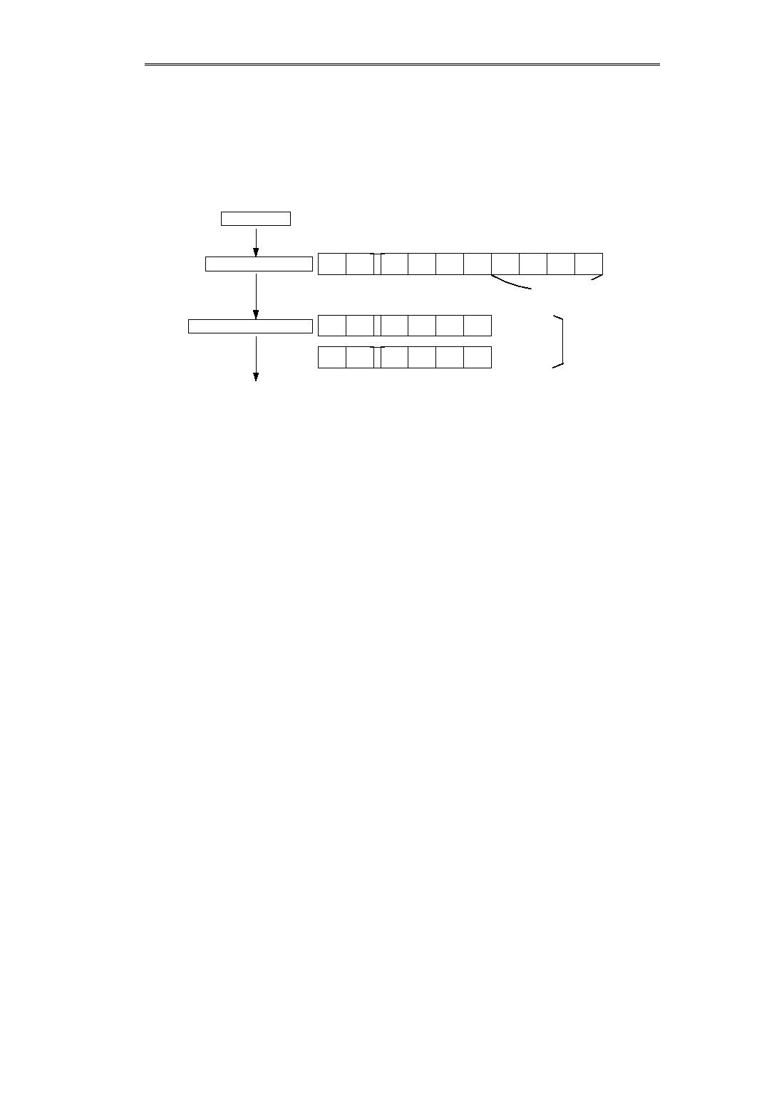
LCD Controller-Driver
S-4561A
Seiko Instruments Inc.
31
<4-Bit Data Length Interface>
When executing a 4-bit operation, it is necessary to set respective functions on a program. After resetting, first write the
upper 4-bits of the function setting command to reset DL (DL = 0). Then this IC is set for the 4-bit data-length interface. Next
write the function setting command again for each upper 4-bits and lower 4-bits to complete the function command. Then
write commands to initialize this IC for 4-bit data-length interface. (See an example shown in the previous page.)
For the 4-bit data-length interface, the upper 4-bits are written first, followed by the lower 4-bits. The RS terminal for register
selection is used to distinguish instruction from data for a command. For the 4-bit data-length interface, do not change the
RS signal during the period when both the upper and lower 4-bits are written.
For the 4-bit data-length interface, open the lower 4-bit terminals of the data bus (DB3-DB0).
Notice that output short-circuit current will flow at READ phase if they are connected to the power supply (VDD or VSS)
RS
0
RWX
0
DB7
0
DB6
0
DB5
1
DB4
0
DB3
-
DB2
-
DB1
-
DB0
-
8-bit length
DL
Not connected
0
0
0
0
1
0
Upper 4 bits
0
0
0
0
0
-
Lower 4 bits
4-bit length
Function Setting
Reset
Normal Function Setting
R
R
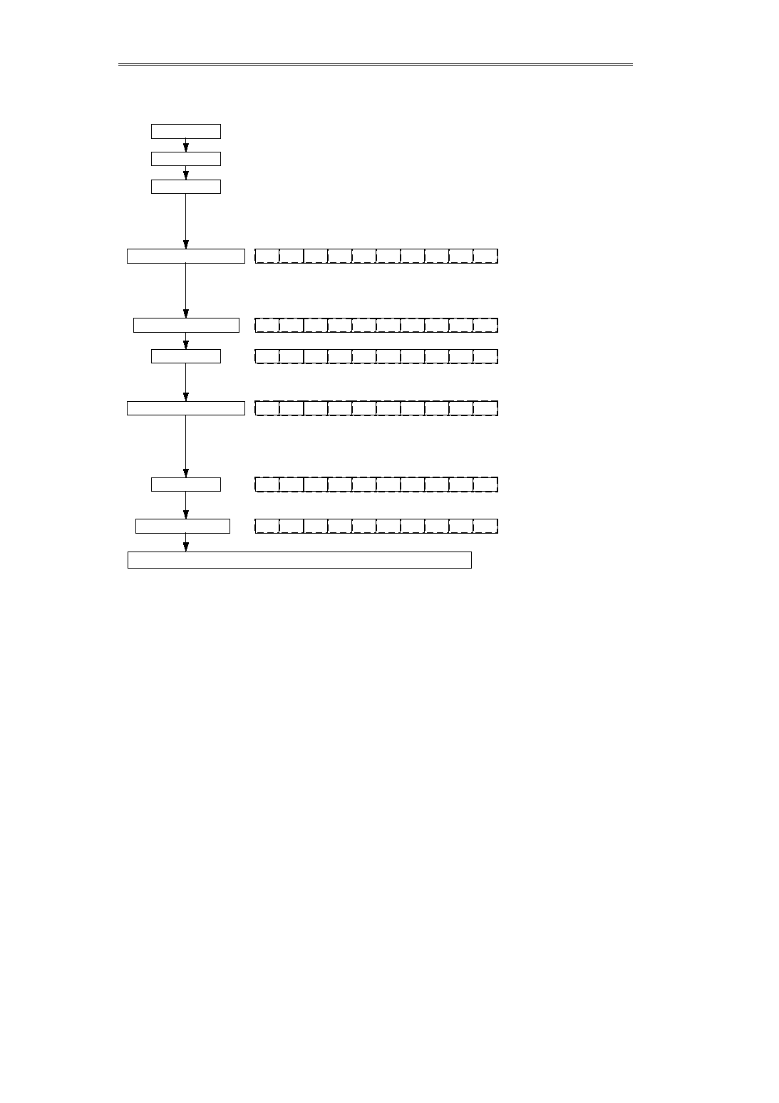
LCD Controller-Driver
S-4561A
32
Seiko Instruments Inc.
4.
Procedures from Powering ON to Display Start
The procedures from powering ON to Display Start are as follows:
Mode Setting Examples after Powering ON
5.
Instruction Execution Time
Any instructions other than the DISPLAY CLEAR are completed within the cycle time (tcyc) represented with the instruction
input timing characteristics. For instance, when the instruction input cycle time is 500
µ
sec, the instruction can be completed
within 500
µ
sec. Consequently, instructions can be input in succession without confirming the BUSY flag. Also, load to the
MPU and the current consumption can be drastically reduced. Inputting the next command within the cycle time is
prohibited.
In the DISPLAY CLEAR mode, it is necessary to write a space code in all of DDRAMs. For the write execution time, refer to
page 18,
"
Instruction Explanation
"
of this specification.
6.
Read and Write Display Data from and In MPU
The Display Data is accessed from the MPU to DDRAM, CGRAM, ICONRAM or ICON BLINK RAM by executing the READ
or WRITE command following the ADDRESS SETTING command of individual RAMs. Always execute the ADDRESS
SETTING command before executing the READ command. When the ADDRESS SETTING command is not executed,
correct display data cannot be read. After executing the READ or WRITE command, the column address is incremented or
decremented depending upon the value of the ID of the ENTRY MODE Setting. Consequently, when the cycle time
represented
q
DL=1
8-bit data length
interface
q
N=0
2-line x 12-column
q
MS=0
Normal Instruction
q
DT=0
5-dot font
0
Setting Examples:
RS
0
R/WX
0
DB7
0
DB6
1
DB5
1
DB4
0
DB3
0
DB2
0
DB1
-
DB0
0
0
0
0
0
0
1
1
1
0
0
0
0
0
1
1
0
1
0
-
q
DL=1
8-bit data length
interface
q
N=0
2-line x 12-column
q
MS=1
Extended Instruction
q
DT=0
5-dot font
Normal Function Setting
0
0
0
0
0
0
0
1
0
0
Powering ON
RESX Input
Wait Time
Initialize.
Wait for BUSY cancellation.
When you do not want monitor BUSY*, wait for 2.0 msec at f
osc
=34 kHz.
Extended Function Setting
q
ID=0
Decrement
q
S=0
No Display Shift
Display ON/OFF
q
D=1
Display ON
q
C=1
Cursor Display ON
q
B=0
Cursor Blink OFF
Entry Mode Setting
Power Save Release
0
0
0
0
0
0
0
0
0
0
q
PS=0
Power Save Cancel
*
Set the wait time twice as long as f
osc
35 clock.
When BUSY is canceled, this IC is set to the power save mode (PS=1) .
Bias Select
0
0
0
1
0
1
0
0
-
1
q
MLC=0
No COM output inversion
q
MLS=0
No SEG output inversion
q
BS5=1 1/5 bias
Write in the specified instruction set, CGRAM, DDRAM, and ICONRAM.
LCD Controller-Driver
S-4561A
Seiko Instruments Inc.
33
7.
Dot Display Mode
5- or 6-dot display mode can be selected by the FUNCTION SETTING command. The 5-dot display mode is used for the dot
matrix for every character; and the 6-dot display mode is used for a full dot matrix.
Display data written in the CGRAM, ICONRAM or other RAM on the 5-or 6-dot display mode is for every 5 bits, and there is
no change in the data length regardless of the dot display mode. The 6-dot display mode controls data inside the IC so that
left one column of each for every character is NOT-LIT. The cursor for the 6-dot display mode appears on the 8th line of the
character in a 5-dot size.
Character Display Example for Every Dot Display Mode
Difference of Display Area for Every Dot Display Mode
5-dot mode display area
6-dot mode display area
2-line x 12-column+ 4-column non-displayed character
2-line x 10-column+ 6-column non-displayed character
1-line x 24-column+ 8-column non-displayed character
1-line x 20-column+ 12-column non-displayed character
8.
Smooth Scroll
Right and left smooth scroll for every dot is possible by executing one ore more command. The lines to be scrolled smoothly
can be selected freely and two lines can be scrolled at the same time.
Smooth scrolling is possible in both 5- and 6-dot display modes. In the 5-dot display mode smooth scroll, individual space
rows are inserted between characters. This allows for easy-to-see smooth scroll display without deformation in characters.
Also, the cursor and the blink shift together with characters.
Smooth Scroll Examples
5-dot display mode
6-dot display mode
5-dot smooth scroll
6-dot smooth scroll
No Shift
1 dot shifts left
2 dot shifts left
3 dot shifts left
4 dot shifts left
5 dot shifts left
Dots corresponding to 1
character shift left
LCD Controller-Driver
S-4561A
34
Seiko Instruments Inc.
Examples of Smooth Scroll of 2nd Lines of a 5-Dot 2-Line x 12-Column Display
9.
Icon Only Display
Regardless of the contents of the display data RAM (DDRAM), the icon only is displayed and the LCD panel is compelled to
be off. Since the contents of the DDRAM do not change, the state is returned to the original display by canceling the Icon
Only Display mode. While the icon only is being displayed, the LCD panel is driven at low power consumption. This allows
for the reduction in the boosting level and also the reduction in the current consumption. Four levels of booster drive
frequency can be selected by the lower 2 bits of the ICON ONLY DISPLAY command (refer to Instruction Explanation: page
18). The booster drive frequency differs depending upon the size of the LCD panel and wiring capacity. Determine the
appropriate frequency on the actual LCD panel.
10. Power Save
After inputting the POWER SAVE command, the CR oscillating circuit and the LCD power supply circuit stop, and the
current consumption of the IC goes down nearly to the value during standstill simultaneously with display OFF. This is valid
for reducing the current consumption when the display is not needed or during wait.
The DDRAM and instruction state still remains unchanged and is returned to the original display by canceling the Power
Save.
11. Connection to LCD
Common output terminals are mounted on both right and left of the chip. Common wiring is needed with respect to the
panel configuration and also display columns.
0
RS
0
R/WX
0
DB7
0
DB6
1
DB5
1
DB4
0
DB3
1
DB2
0
DB1
-
DB0
q
Extended Instruction Select
q
2nd Line Select
0
0
1
0
0
1
-
-
1
0
q
1 dot shifts left
0
0
1
0
0
1
-
0
0
1
q
2 dots shift left
0
0
1
0
0
1
-
0
1
0
q
3 dots shift left
0
0
1
0
0
1
-
0
1
1
q
4 dots shift left
0
0
1
0
0
1
-
1
0
0
q
5 dots shift left
0
0
1
0
0
1
-
1
0
1
q
1 character shifts left
(6 dots shift left)
0
0
1
0
1
0
0
0
0
1
q
1 dot shifts left
(7 dots shift left)
0
0
1
0
0
1
-
0
0
1
q
2 dots shift left
(8 dots shift left)
0
0
1
0
0
1
-
0
1
0
q
15 characters shift left
(90 dots shift left)
0
0
1
0
1
0
1
1
1
1
q
5 dots shift left
(95 dots shift left)
0
0
1
0
0
1
-
1
0
1
q
No character shifts
(Original Display Position)
0
0
1
0
1
0
0
0
0
0
Remarks
R
After Dot Shift, set a wait time for the next shift so as to make the display legible.
R
To execute the Smooth Scroll, shift characters left by the amount corresponding to the display column
(including non-displayed characters) and input the instruction so that the amount of the shift is reduced.
LCD Controller-Driver
S-4561A
Seiko Instruments Inc.
35
s
Examples of Connection to LCD Panel
1. When the IC is mounted from the front view (Viewing Side):
2-line
×
12-character
LCD
17
×
60
9
10
:
16
Icon
1
2
:
8
SEG
S-4561A
COMICN2
COMICN1
COM
9 to 16
COM
1 to 8
MLC=0
MLS=0
16
:
10
9
8
:
2
1
S-4561A
1
2
:
8
9
10
:
16
SEG
2-line
×
12-character
LCD
17
×
60
Icon
9
10
:
16
Icon
1
2
:
8
COMICN2
COM
9 to 16
COMICN1
COM
1 to 8
MLC=1
MLS=1
1-line
×
24-character LCD 9
×
120
Icon
1
2
:
8
Icon
1
2
:
8
SEG
S-4561A
COM
9 to 16
COM
1 to
8
MLC=0
MLS=0
COMICN1
COMICN2
8
:
2
1
1, 2,
60
16
:
10
9
1-line
×
24-character LCD 9
×
120
61, 62,
120
SEG
S-4561A
9
10
:
16
60,
, 2 , 1
1
2
:
8
COM
9 to 16
COMICN2
MLC=1
MLS=1
COM
1 to 8
COMICN1
Icon
1
2
:
8
Icon
1
2
:
8
1, 2,
60
1, 2,
60
60,
,2 , 1
1, 2,
60
1, 2,
60
1, 2,
60
61, 62,
120
Viewing Side
Rear Side of IC
N=0: 2 -line x 12 -character LCD panel
Icon
N=1: 1-line 24 -character LCD panel
Figure 12: 2-line x 12-character LCD panel
Figure 13: 1-line x 24-character LCD panel
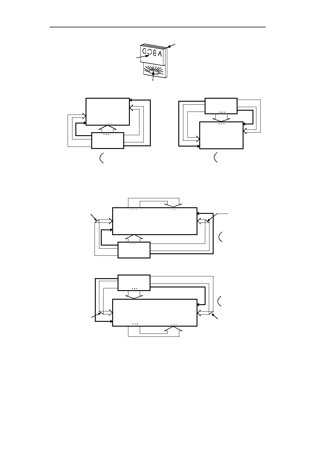
LCD Controller-Driver
S-4561A
36
Seiko Instruments Inc.
2. When the IC is mounted from the rear side:
2-line
×
12-character
LCD
17
×
60
Icon
9
10
:
16
Icon
1
2
:
8
SEG
S-4561A
COMICN2
COMICN1
COM
1 to 8
COM
9 to 16
MLC=0
MLS=1
8
:
2
1
16
:
10
9
S-4561A
1
2
:
8
9
10
:
16
SEG
2-line
×
12-character
LCD
17
×
60
Icon
9
10
:
16
Icon
1
2
:
8
COMICN1
COM
9 to 16
COMICN2
COM
1 to 8
MLC=1
MLS=0
1-line
×
24-character LCD 9
×
120
Icon
1
2
:
8
Icon
1
2
:
8
SEG
S-4561A
MLC=1
MLS=1
COMICN2
8
:
2
1
16
:
10
9
1-line
×
24-character LCD 9
×
120
61, 62,
120
SEG
S-4561A
9
10
:
16
1
2
:
8
COM
1 to 8
COMICN1
MLC=0
MLS=0
COM
9 to 16
COM
9 to 16
Reverse
COMICN1
COM
1 to 8
Reverse
Reverse
COMICN2
Reverse
1, 2,
60
60,
,2 , 1
1, 2,
60
1, 2,
60
1, 2,
60
61, 62,
120
60,
,2 , 1
1, 2,
60
1, 2,
60
Icon
1
2
:
8
Icon
1
2
:
8
Viewing Side
Rear Side
Rear Side of IC
N=0: 2 -line x 12 -character LCD panel
N=1: 1 -line
×
24 -character LCD panel
Figure 14: 2-line x 12-character LCD panel
Figure 15: 1-line x 24-character LCD panel
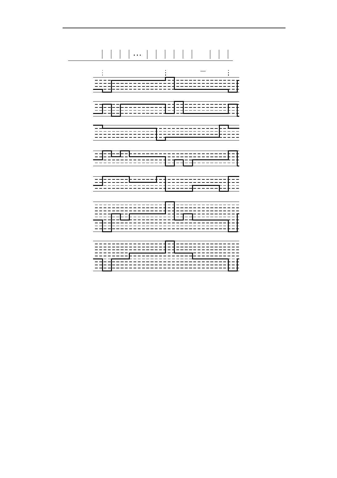
LCD Controller-Driver
S-4561A
Seiko Instruments Inc.
37
s
Examples of LCD Drive Output Waveform
COM
1
COM
2
SEG
1
SEG
2
COM
1
COM
1
- SEG
1
- SEG
2
Figure 16 Example of LCD Drive Output Waveform (1/5 bias)
V
LCD
V
1
V
2
V
3
V
4
V
SS
V
LCD
V
1
V
2
V
3
V
4
V
SS
- V
4
- V
3
- V
2
- V
1
- V
LCD
V
LCD
V
1
V
2
V
3
V
4
V
SS
1/17 Duty Common
Output Terminal
1
2
3
16
ICN1
ICN2 1
2
3
16
fosc=34 kHz
Frame Frequency=76.9 Hz
COMICN
M
M
COM
ICN1
ICN2
COM
V
LCD
V
1
V
2
V
3
V
4
V
SS
V
LCD
V
1
V
2
V
3
V
4
V
SS
V
LCD
V
1
V
2
V
3
V
4
V
SS
- V
4
- V
3
- V
2
- V
1
- V
LCD
V
LCD
V
1
V
2
V
3
V
4
V
SS
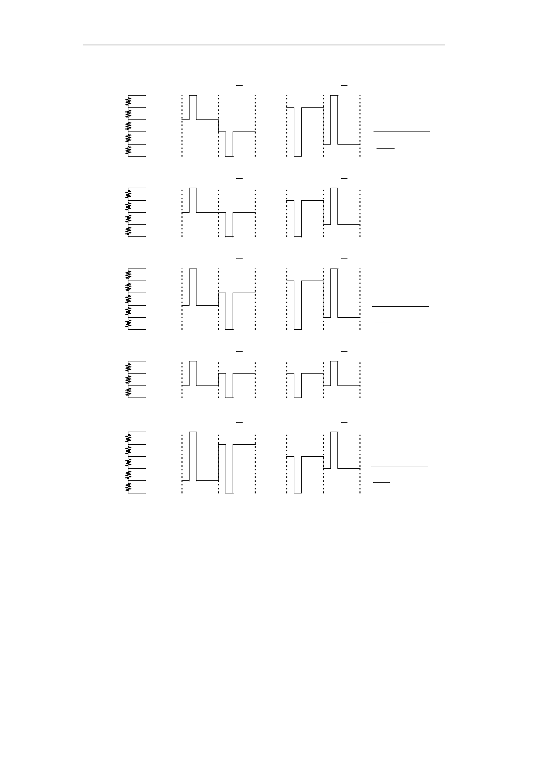
LCD Controller-Driver
S-4561A
38
Seiko Instruments Inc.
s
External Bias Resistor vs LCD Drive Waveform
Figure 17 External Bias Resistor vs LCD Drive Waveform
V
LCD
V
1
V
2
V
3
V
4
V
SS
SEG Waveform
M
M
1.
1/4 or more bias
COM Waveform
M
M
Ra
2
R
b
V
LCD
V
1
V
2
=V
3
V
4
V
SS
SEG Waveform
M
M
2.
1/4 bias
COM Waveform
M
M
R
b
R
b
R
b
V
LCD
V
1
V
3
V
2
V
4
V
SS
SEG Waveform
M
M
3.
1/3 to 1/4 bias
COM Waveform
M
M
R
c2
R
c3
R
c2
R
d
V
LCD
V
1
=V
3
V
2
=V
4
V
SS
SEG Waveform
M
M
4.
1/3 bias
COM Waveform
M
M
R
d
R
d
R
e1
V
LCD
V
3
V
1
V
4
V
2
V
SS
SEG Waveform
M
M
5.
1/2 to 1/3 bias
COM Waveform
M
M
R
e2
R
e3
R
e2
R
e1
R
a2
=
R
a1
0
Bias
=
R
a1
+R
a1
+R
a2
+R
a1
+R
a1
R
a
=
4+
1
R
C2
+R
C3
=R
C1
R
C2
=
R
C1
0
1
Bias
=
R
C1
+R
C2
+R
C3
+R
C2
+R
C1
R
C1
=
3+
1
R
e3
=
(Re
1
+Re
2
)
R
e1
=R
e3
0
1
Bias
=
R
e1
+R
e2
+R
e3
+R
e2
+R
e1
R
e1
+R
e2
=
2+
1
Ra
1
Ra
1
Ra
1
Ra
1
R
c1
R
c1
LCD Controller-Driver
S-4561A
Seiko Instruments Inc.
39
s
Absolute Maximum Ratings
Table 27 Absolute Maximum Ratings
V
DD
=0.0 V
Remarks:
R
If your IC is used in the range exceeding the above absolute maximum ratings, IC
'
s characteristics may
drastically deteriorate and may lead to a breakdown of the device.
R
Use this IC within the specified range of electrical characteristics. If not, the functions and reliability of the IC
cannot be assured.
R
When connecting a bias resistor externally, determine the LCD power supply voltage so that its state goes to
V
LCD
V
DD
during display.
R
Notice that isolation of the IC from light exposure is not taken iinto account for this IC design.
s
DC Characteristics
1. Electrical Characteristics
Table 28 Electrical Characteristics
(Unless otherwise specified: V
SS
=0 V, V
DD
=3.0
±
0.3 V, Ta=-30 to 85
°
C)
Parameter
Symbol
Ratings
Unit
Supply voltage
V
DD
-0.4 to +7.0
V
LCD drive voltage 1
V
LCD
-0.4 to +8.0
V
LCD drive voltage 2
V
1
, V
2
, V
3
, V
4
V
LCD
-0.4
V
Input voltage
V
IN
-0.4 to V
DD
+0.4
V
Output voltage
V
OUT
-0.4 to V
DD
+0.4
V
Operating temperature range
T
opr
-30 to +85
°
C
Storage
Chip
T
stg
-55 to +125
°
C
temperature range
TCP
-55 to +100
Parameter
Symbol
Conditions
Min.
Typ.
Max.
Unit
Note
Operating Voltage 1
V
DD1
Internal booster is used.
2.4
-
3.6
V
Note 1
Operating Voltage 2
V
DD2
External LCD power supply is
used.
2.4
-
5.5
V
Note 1
Note 2
High-level Input Voltage
V
IH
0.8
×
V
DD
-
V
DD
V
Note 3
Low-level Input Voltage
V
IL
V
SS
-
0.2
×
V
DD
V
Note 3
High-level Output Voltage
V
OH1
I
OH
=-0.5 mA
0.8
×
V
DD
-
-
V
Note 4
V
OH2
I
OH
=-50
µ
A
0.8
×
V
DD
-
-
V
OSC2
Low-level Output Voltage
V
OL1
I
OL
=0.5 mA
-
-
0.2
×
V
DD
V
Note 4
V
OL2
I
OL
=50
µ
A
-
-
0.2
×
V
DD
V
OSC2
Pull-up Current
I
U
Ta=25
°
C, V
DD
=3.0 V
-20
-10
-4
µ
A
RESX
Input Leak Current
I
ILEAK
-1.0
-
1.0
µ
A
Note 5
Output Current
I
OLEAK
-3.0
-
3.0
µ
A
Note 6
LCD Driver ON Resistor
R
ON
Ta=25
°
C, V
LCD
=5.0 V
1/4-bias
-
3.0
5.0
k
Note 7
Current Consumption During
Standstill
I
S
Power Save
-
0.05
5.0
µ
A
Note 8
I
DD1
Internal booster is used:
During LC display
Rf=500 k
V
OUT
=6.0 V V
LCD
=5.0 V
-
70.0
105.0
µ
A
Note 9
Operating Current
I
DD2
External LCD power supply is
used:
During LC display
Rf=500 k
V
LCD
=5.0 V
-
15.0
20.0
µ
A
Note 10
Oscillating Frequency
f
OSC
R
f
=500 k
V
DD
=3.0 V
27
34
41
kH
Z
Reset Time
t
R
10
-
-
µ
s
Note 11
Reset Pulse Width
t
RW
20
-
-
µ
s
Note 12
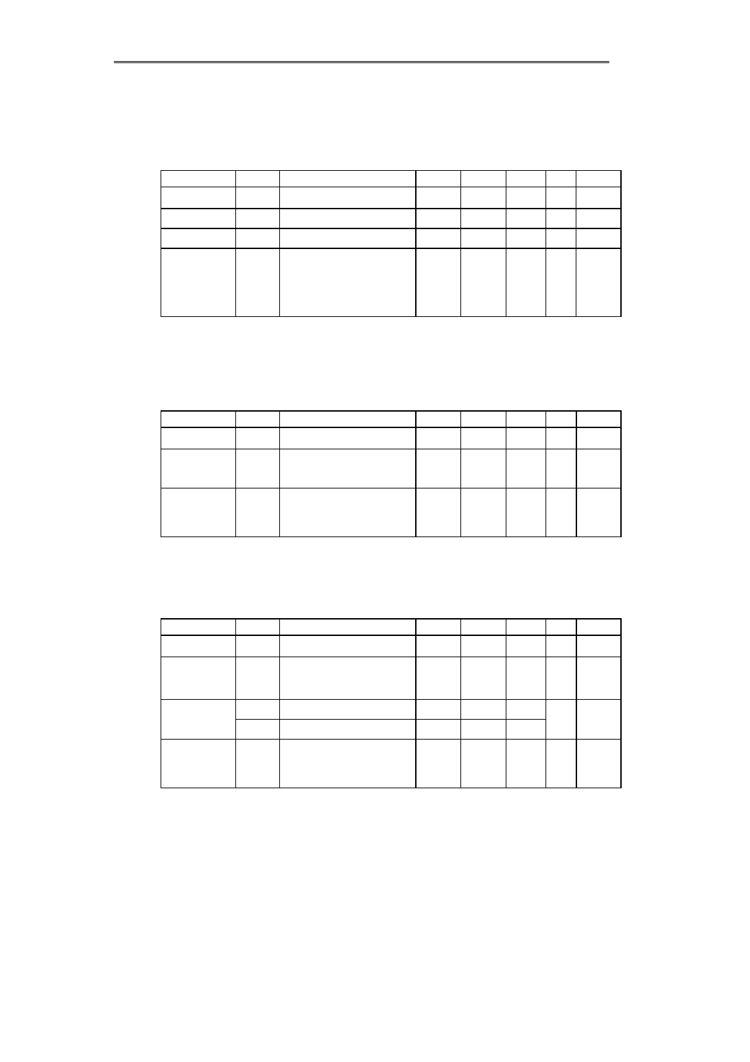
LCD Controller-Driver
S-4561A
40
Seiko Instruments Inc.
2. LCD Power Supply Circuit Electrical Characteristics
2.1 When Using an Internal Booster: FNC1=
"
H,
"
FNC2=
"
H
"
Table 29
Electrical Characteristics
V
SS
=0 V, V
DD
=3.0
±
0.3 V, Ta=-30 to 85
°
C
2.2 When Using an External LCD Power Supply: FNC1=
"
L,
"
FNC2=
"
L
"
Table 30
Electrical Characteristics
V
SS
=0 V, VDD=3.0
±
0.3V, Ta=-30 to 85
°
C
2.3 When Using an External Bias: FNC1=
"
H,
"
FNC2=
"
L
"
Table 31
Electrical Characteristics
V
SS
=0 V, VDD=3.0
±
0.3 V, Ta=-30 to 85
°
C
Parameter
Symbol
Conditions
Min.
Typ.
Max.
Unit
Note
Operating Voltage
1
V
DD1
FNC1=
"
H
"
, FNC2=
"
H
"
2.4
-
3.6
V
Note 13
Boosting Output
Voltage
V
OUT
4.8
-
7.2
V
Voltage Regulator
Output Voltage
V
LCD1
2.7
-
6.5
V
Note 14
LCD Power
Supply Circuit
Current
Consumption 1
I
LCD1
V
OUT
=6.0 V Double boosting
V
DD
=3.0 V
V
LCD
=5.0 V 1/4 bias
Oscillating Frequency 34 kHz
Display ON, Checker Display
No Load of LCD Power Supply
Circuit
55.0
85.0
µ
A
Note 15
Parameter
Symbol
Conditions
Min.
Typ.
Max.
Unit
Note
Operating Voltage
2
V
DD2
FNC1=
"
L
"
, FNC2=
"
L
"
2.4
-
5.5
V
Note 16
LCD Power
Supply Circuit
Operating Voltage
2
V
LCD2
FNC1=
"
L
"
, FNC2=
"
L
"
2.7
-
6.5
V
Note 17
LCD Power
Supply Circuit
Current
Consumption 2
I
LCD2
V
LCD2
=5.0 V 1/4-bias
Oscillating Frequency 34 kHz
Display ON, Checker Display
No Load of LCD Power Supply
Circuit
28.0
45.0
µ
A
Note 18
Parameter
Symbol
Conditions
Min.
Typ.
Max.
Unit
Note
Operating Voltage
Range 2
V
DD2
FNC1=
"
H
"
, FNC2=
"
L
"
2.4
-
5.5
V
Note 19
LCD Power
Supply Circuit
Voltage 3
V
LCD3
FNC1=
"
H
"
FNC2=
"
L
"
2.7
-
6.5
V
Note 20
Bias Voltage
V
1,
V
3
1.2
-
V
LCD3
-0.4
V
Note 21
Input Voltage
V
2,
V
4
0.4
-
V
LCD3
-1.2
LCD Power
Supply Circuit
Current
Consumption 3
I
LCD3
V
LCD3
=3.0V 1/3-bias
Oscillating Frequency 34 kHz
Display ON, Checker Display
No Load of LCD Driver
10.0
15.0
µ
A
Note 22
LCD Controller-Driver
S-4561A
Seiko Instruments Inc.
41
2.4 Reference Voltage Circuit
Table 32
Reference Voltage
V
SS
=0 V, V
DD
=3.0
±
0.3 V, Ta=25
°
C
3. Reference
Table 33
Input Pin Capacity
Parameter
Symbol
Conditions
Min.
Typ.
Max.
Unit
Note
Input Pin Capacity
C
IN
Ta=25
°
C
-
5
8
pF
Note 4
Note 1
Sharp variation in the supply voltage or input signal voltage due to strange noises may lead to a malfunction of
the IC. Supply stable supply voltage and input signal voltage.
If you change the level of the supply voltage intentionally, a malfunction may occur. NEVER change the level of
the supply voltage.
Note 2
The maximum operating voltage of the logic is 5.5 V when an internal booster is not used.
Note 3
Pins RS, E, RWX, RESX, C86, P/SX, OSC1, FNC1, and FNC 2.
Pins D0 to D7 during display data write and command input.
Fully swing the levels VIH and VIL of the input signal within the range of power supply voltage so that the state is
VIH=VDD, VIL=VSS. When the level of VIH and VIL is the middle level of the supply voltage, the through-
current flowing through the input pin as well as the current consumption may be increased.
Note 4
Pins D0 to D7.
Note 5
Pins RS, E, RWX, RESX, C86, P/SX, FNC1, and FNC 2.
Note 6
Pins D0 to D7 during write and high-impedance.
Note 7
ON resistance between LCD drive output pins (SEG1 to SEG60, COM1 to COM16) and LCD drive bias voltage
pins (V1, V2, V3, V4). Measure the current which flows after applying a 0.1-V difference between the LCD
drive bias voltage pins (V1, V2, V3, V4) and LCD drive output pins in the external VLCD voltage input mode
(FNC1, 2=
"
HL
"
).
Note 8
Power save state. When turning the input pin to
"
Floating,
"
the through-current flows. Connect and fix the input
pins to VSS or VDD.
Note 9
Shows the current consumption during display including CR oscillation.
It includes the current consumed by the booster, LCD supply voltage adjustment circuit, voltage regulator, LCD
bias resistor when using the internal booster. The LCD drive output pin is no load. It does not include the
current consumed by the LCD panel and wiring capacitor. Measure it without access from the MPU.
Note 10
Shows the current consumption only for the logic during display including CR oscillation.
It does not include the current consumed by the LCD power supply systems, such as the booster, LCD supply
voltage adjustment circuit, and voltage regulator, when using the external LCD power supply. The LCD drive
output pin is no load. It does not include the current consumed by the LCD panel and wiring capacitor.
Measure it without access from the MPU.
Note 11
Shows the wait time from when the reset ends at the rising edge of the RESX to when normal operation is
possible.
Note 12
Specifies the minimum reset pulse width.
Note 13
Since the maximum output voltage of the booster is 7.2 V, the maximum operating voltage of the LCD power
supply circuit including the logic and the booster is 3.6 V.
Parameter
Symbol
Conditions
Min.
Typ.
Max.
Unit
Note
Reference Voltage
V
REF
V
REF
=0.01% /
°
C
1.3
1.7
2.1
V
Note 23
V
REF
=- 0.13% /
°
C
1.3
1.7
2.1

LCD Controller-Driver
S-4561A
42
Seiko Instruments Inc.
Note 14
Set output voltage VLCD of the voltage regulator so that VOUT - V LCD
0.2 V and the output voltage is 6.0 V at
maximum.
Note 15
Shows the value of the current consumed by the booster, voltage regulator, voltage follower, internal bias
resistor, and LCD driver. It does not include the value IRREG=V5/(R1+R2+R3) of the current flowing through
external resistors R1, R2, and R3. Also, it does not include the value of the current consumed by the LCD panel.
All of the current consumed during display are IDD1. Current consumed by the logic is IDD2. ILCD1 cannot be
measured. ILCD1 - IDD2 is equivalent to ILCD1.
Note 16
Since the booster is not used, the maximum operating voltage of the logic is 5.5 V.
Note 17
Shows the operating voltage range of the voltage follower, internal bias resistor, and LCD driver.
Note 18
Shows the current consumed by the voltage follower, internal bias resistor, and LCD driver. It does not include
the current consumed by the LCD panel. The current consumed during display is IDD2 + ILCD2. The current
consumed by only the logic is ILCD2.
Note 19
Since the booster is not used, the maximum operating voltage of the logic is 5.5 V.
Note 20
Shows the operating voltage range of the voltage follower and LCD driver.
Note 21
V1, V2, V3 and V4 are limited by the voltage level within the input voltage range. Therefore, the bias ratio can be
freely determined.
Note 22
Shows the current consumed by the voltage follower and LCD driver. It does not include the current consumed
by the LCD panel. The current consumed during display is IDD2 + ILCD3. The current consumed by only the
logic is ILCD2.
Note 23
Shows different characteristics depending upon the temperature coefficient selected by the corresponding
command.
Note 24
When the frame frequency and the fluorescent lamp
'
s frequency are the same, the display screen may flicker.
Taking into consideration fluctuation in the IC and the oscillating resistor, as well as the temperature
characteristics, determine the appropriate oscillating frequency.
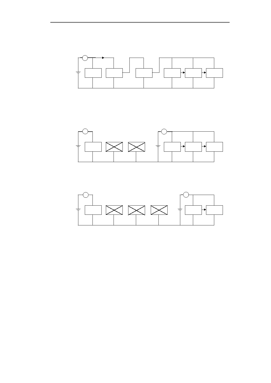
LCD Controller-Driver
S-4561A
Seiko Instruments Inc.
43
s
Current Consumption Measurement Examples
1.
Current Consumption of (FNC1, 2=
"
H H
"
) when using a booster:
2.
Current Consumption of (FNC1, 2=
"
L L
"
) when using an external power supply:
3.
Current Consumption of (FNC1, 2=
"
H L
"
) when using an external bias resistor:
LCD
Driver
VF
Bias
Resistor
VREG
Booster
Logic
I
DD1
I
LCD1
V
OUT
V
LCD
V
DD
Remark:
The current consumed by the LCD power supply circuit I
LCD1
cannot be measured. It is
equivalent to I
LCD1
= I
DD1
- I
DD2
.
LCD
Driver
VF
Bias
Resistor
VREG
Booster
Logic
I
DD2
V
DD
I
LCD2
V
LCD2
Figure 18 Current Consumption Measurement Examples
LCD
Driver
VF
Bias
Resistor
VREG
Booster
Logic
I
DD2
V
DD
I
LCD3
V
LCD3
Remark: VREG:
Voltage
Regulator
VF:
Voltage Follower
A
A
A
A
A
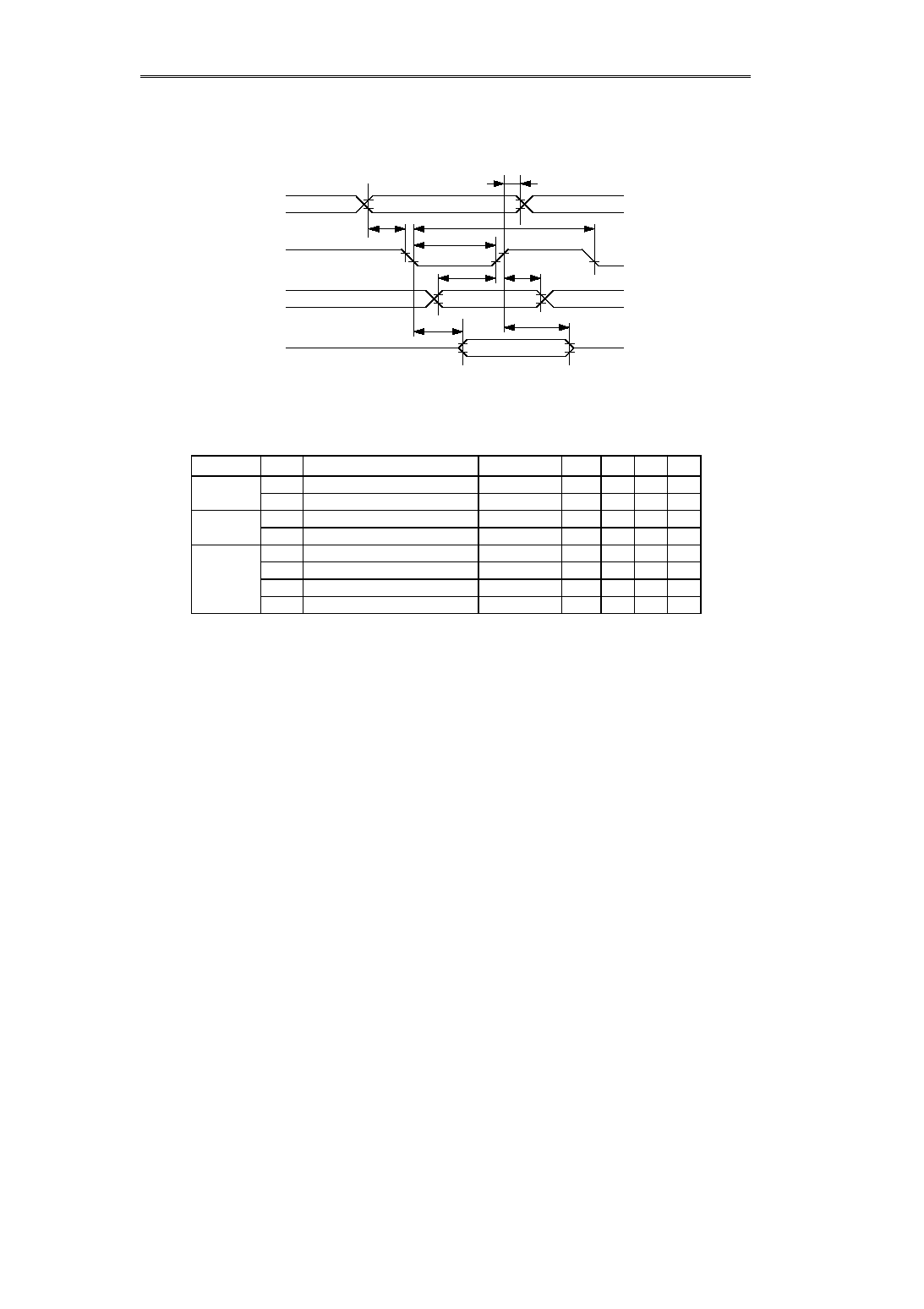
LCD Controller-Driver
S-4561A
44
Seiko Instruments Inc.
s
Timing Characteristics
1. Parallel Interface
1.1 80-Family MPU Read/Write Timing Characteristics
Table 34 80-Family MPU Read/Write Timing Characteristics When VDD=3 V
(Ta=-30 to 85
°
C, V
DD
=3.0
±
0.3 V)
Signal
Symbol
Designation
Conditions
Min.
Max.
Unit
Note
RS
t
AH8
Address Hold Time
40
ns
t
AW8
Address Setup Time
40
ns
E, RWX
t
CYC8
System Cycle Time
1000
ns
t
CC8
Control Pulse Width
200
ns
t
DS8
Data Setup Time
160
ns
D
0
to D
7
t
DH8
Data Hold Time
40
ns
t
ACC8
Data Read Access Time
CL=15 pF
180
ns
t
OH8
Output Disable Time
CL=15 pF
10
120
ns
Remarks:
R
Rise/fall time of the input signal is 15 sec. or less.
R
Timing is specified at 20% or 80% of the signal waveform.
t
AW8
t
CC8
t
CYC8
t
AH8
t
DS8
t
DH8
t
ACC8
t
OH8
RS
E, RWX
D
0
to D
7
(WRITE)
D
0
to D
7
(READ)
Figure 19 80-Family MPU Read/Write Timing Characteristics
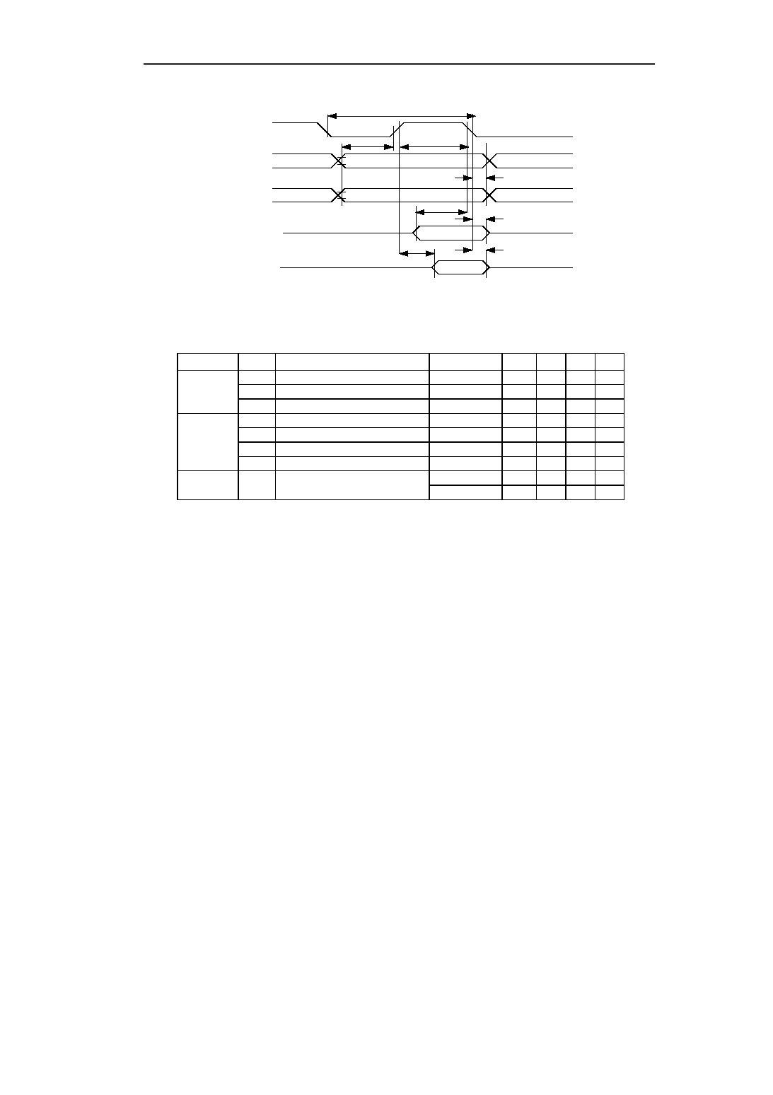
LCD Controller-Driver
S-4561A
Seiko Instruments Inc.
45
1.2 68-Family MPU Read/Write Timing Characteristics
Figure 20 68-Family MPU Read/Write Timing
Table 35 68-Family MPU Read/Write Timing Characteristics When VDD=3 V
(Ta=-30 to 85
°
C, VDD=3.0
±
0.3 V)
Remarks:
R
Rise/fall time of the input signal is 15 sec. or less.
R
Timing is specified at 20% or 80% of the signal waveform.
Signal
Symbol
Designation
Conditions
Min.
Max.
Unit
Note
t
CYC6
System Cycle Time
1000
ns
RS, RWX
t
AH6
Address Hold Time
40
ns
t
AW6
Address Setup Time
40
ns
t
DS6
Data Setup Time
160
ns
D
0
to D
7
t
DH6
Data Hold Time
40
ns
t
ACC6
Access Time
CL=15 pF
180
ns
t
OH6
Output Disable Time
CL=15 pF
10
120
ns
E
t
EW
Enable Pulse Width
READ
200
ns
WRITE
160
ns
t
AW6
t
CYC6
t
ACC6
E
D0 to D7
(WRITE)
t
EW
t
AH6
t
DH6
t
OH6
t
DS6
RWX
RS
DB0 to
(READ)
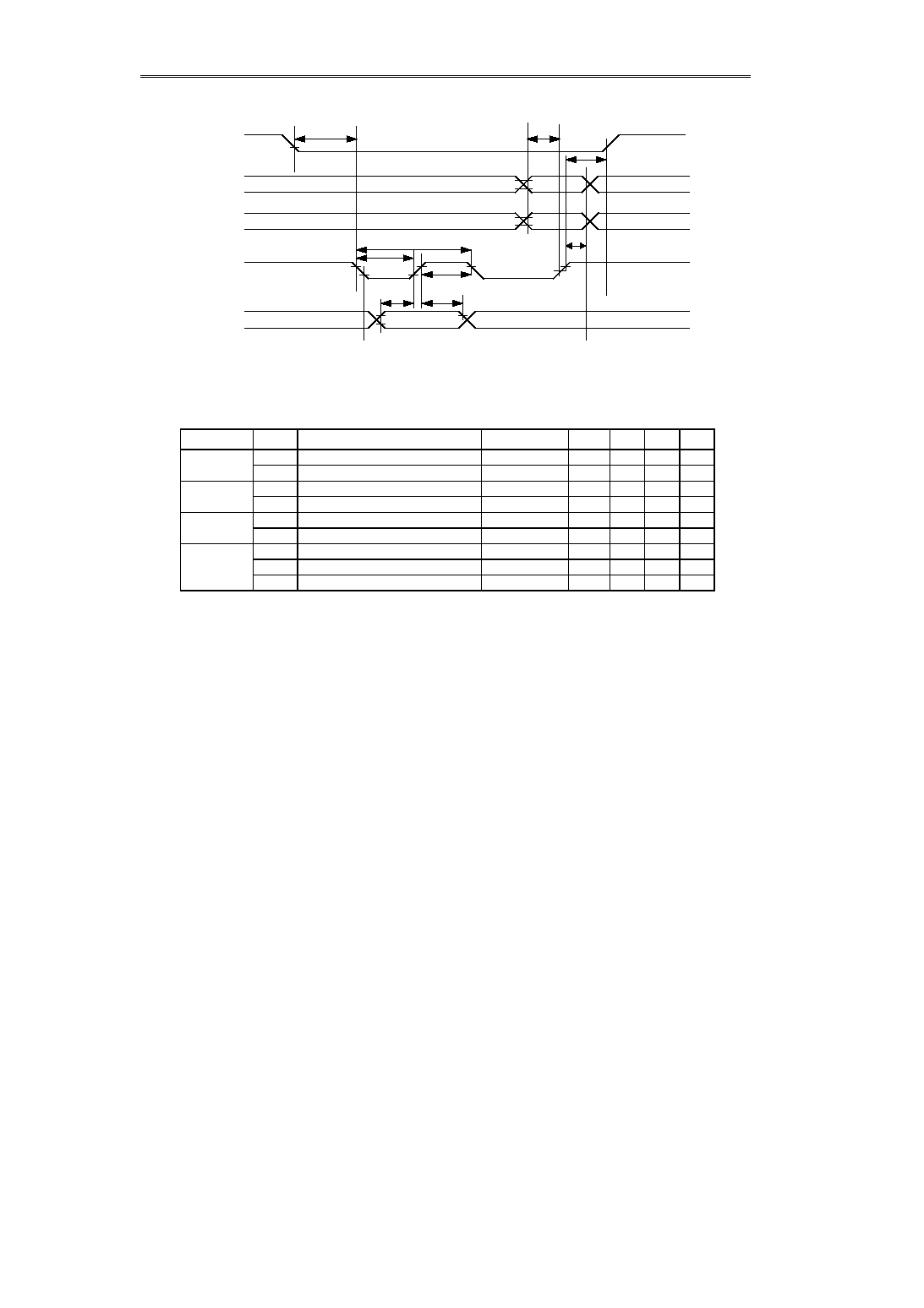
LCD Controller-Driver
S-4561A
46
Seiko Instruments Inc.
2. Serial Interface
Table 36 Serial Interface Timing Characteristics When VDD=3V
(Ta=-30 to 85
°
C, V
DD
=3.0
±
0.3 V)
Remarks:
R
Rise/fall time of the input signal is 15 sec. or less.
R
Timing is specified at 20% or 80% of the signal waveform.
Signal
Symbol
Designation
Conditions
Min.
Max.
Unit
Note
E
t
CSS
Chip Select Setup Time
0
ns
t
CHS
Chip Select Hold Time
50
ns
RS, RWX
t
ASS
Address Setup Time
50
ns
t
AHS
Address Hold Time
50
ns
D0
t
DSS
Data Setup Time
50
ns
(SDI)
t
DHS
Data Hold Time
50
ns
D1
t
CYCS
Clock Cycle Time
250
ns
(SCLK)
t
CLLS
Clock L Time
100
ns
t
CLHS
Clock H Time
100
ns
t
CSS
t
CLLS
t
CYCS
t
CHS
t
AHS
t
CLHS
t
DHS
t
DSS
E
D1
(SCLK)
D0
(SDI)
RS
RWX
t
ASS
Figure 12 Serial Interface Read/Write Timing
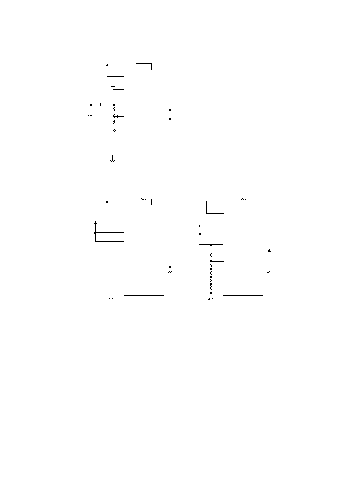
LCD Controller-Driver
S-4561A
Seiko Instruments Inc.
47
s
Examples Application Circuits
FNC1
FNC2
FNC1
V
SS
V
DD
C1
Rf
OSC2
OSC1
V
DD
C+
C-
V
OUT
V
LCD
V
CNT
V1
V2
V3
V4
FNC2
FNC1
Rf
OSC2
OSC1
FNC2
OSC2
OSC1
V
DD
V
SS
V
SS
V
DD
C1
R2
R1
C2
R3
V
SS
V
SS
V
DD
V
DD
C+
C-
V
OUT
V
LCD
V
CNT
V1
V2
V3
V4
V
SS
V
LCD
V
SS
V
DD
C+
C-
V
OUT
V
LCD
V
CNT
V1
V2
V3
V4
V
SS
V
DD
Rf
V
LCD
q
When using an internal LCD power supply circuit (doubler):
q
When using external LCD power supply:
-
Reference -
Rf=500 k
C1= 0.47
µ
F
C2= 1
µ
F
R1+R2+R3 = 2M
q
When an external bias resistor is connected:
Figure 22 Examples Application Circuits
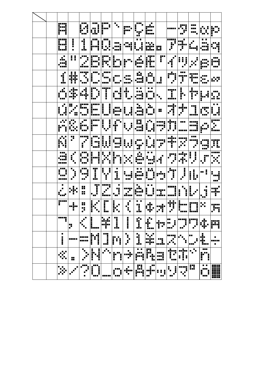
48
Chart 002: Relationship between Character Codes and Character Patterns
Upper
Lower
0000
0001
0010
0011
0100
0101
0110
0111
1000
1001
1010
1011
1100
1101
1110
1111
0000
0001
0010
0011
0100
0101
0110
0111
1000
1001
1010
1011
1100
1101
1110
1111
CG
RAM
(1)
CG
RAM
(2)
CG
RAM
(3)
CG
RAM
(4)
CG
RAM
(5)
CG
RAM
(6)
CG
RAM
(7)
CG
RAM
(8)
CG
RAM
(1)
CG
RAM
(2)
CG
RAM
(3)
CG
RAM
(4)
CG
RAM
(5)
CG
RAM
(6)
CG
RAM
(7)
CG
RAM
(8)