
Contents
Features.............................................................. 1
Applications......................................................... 1
Block Diagram..................................................... 1
Pin Assignment ................................................... 1
Pin Function ........................................................ 2
Command Configuration ..................................... 2
Data Configuration .............................................. 3
Ordering Information ........................................... 3
Absolute Maximum Ratings................................. 3
Recommended Operating Conditions ................. 4
DC Characteristics .............................................. 4
Oscillation Characteristics ................................... 5
AC Characteristics 1 (S-3510ANFJX,
S-3510AEFJX, RL1=30 k
W
, CL1=50 pF) ............ 6
AC Characteristics 2 (S-3510ACFJX,
S-3510ADFJX, CL1=50 pF) ................................ 6
AC Characteristics 3 (S-3510ACFJX,
S-3510ADFJX, CL1=50 pF) ................................ 6
Timing Charts...................................................... 7
Operation ............................................................ 8
Application Circuit Examples ............................... 13
Dimensions ......................................................... 14
Taping Specifications .......................................... 15
Precautions ......................................................... 16
Characteristics .................................................... 17
Frequently Asked Questions................................ 20

Seiko Instruments Inc.
1
The S-3510 is a series of CMOS real-time clock ICs that inputs/ outputs
serial clock or calendar data into/from the CPU.
Features
Applications
Block Diagram
Pin Assignment
REAL-TIME CLOCK
S-3510 Series
Operating power supply:
1.7 V to 5.5 V
Low current consumption: 2.0
�
A typ. at 3.0 V
(S-3510AFFJA : 2.0
�
A typ.
at 3.0 V)
BCD output of second, minute, hour, day, date, month and
year
Easy serial interface to CPU with 3 lines (SIO, SCK, and CS)
Built-in automatic calendar
Built-in voltage detector
Built-in constant voltage circuit
Built-in oscillation circuit (Cg and Cd are built in)
Video cameras
FAXes
Cellular phones
Printers
SIO
Sec.
Min.
Hr.
Day
Date
Mon.
Year
Counter
Sec.
Min.
Hr.
Day
Date
Mon.
Year
Shift Register
Status Register
Serial Interface
&
Controller
SCK
CS
OSC
&
Divider
X
IN
X
OUT
TP
OUT
Voltage
Detector
V
DD
V
SS
Figure 1
TP
OUT
X
OUT
X
IN
V
SS
V
DD
SIO
SCK
CS
1
2
3
4
8
7
6
5
Figure 2
REAL-TIME CLOCK
S-3510 Series
2
Seiko Instruments Inc.
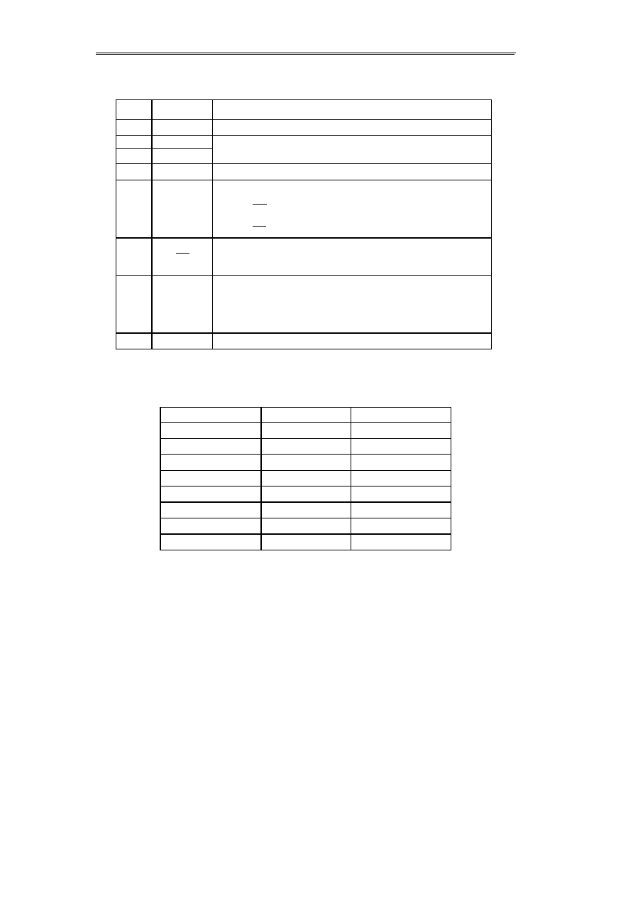
Pin Function
Command Configuration
Table 2
Command
Code
Note
READ 1(Data Read)
1 1 1 0
�
�
�
�
Output from the year data
READ 2(Data Read)
1 1 1 1
�
�
�
�
Output from the day data
WRITE 1(Data Write)
1 0 0 1
�
�
�
�
Input from the year data
WRITE 2(Data Write)
1 0 0 0
�
�
�
�
Input from the day data
STATUS
WRITE
1 0 1 1 D3 D2 D1 D0
Status write
RESET
1 0 1 0 1 0 1 0
Initialization
TEST START
1 1 0 1 0 1 0 1
Test mode start
TEST END
1 1 0 1 1 0 1 0
Test mode end
No.
Name
Function
1
TP
OUT
Standard signal output (Nch open-drain output or CMOS output)
2
X
OUT
Connects to the X
'
ftal resonator (f=32768 Hz)
3
X
IN
[Cg and Cd are built in]
4
V
SS
Power supply (GND)
5
CS
Chip select input (Built-in pull-down resistance)
"
H
"
:
The SIO pin is capable of inputting/outputting data.
The SCK pin is capable of accepting the input.
"
L
"
:
The SIO pin is at Hi-Z.
The SCK pin is not capable of accepting the input.
6
SCK
Clock input:
Inputs and outputs data from the SIO pin in synchronization with the clock. The
clock cannot be accepted when the CS pin is
"
L.
"
7
SIO
Serial data input/output:
When the CS is
"
L,
"
the SIO pin is at
"
Hi-Z.
"
When the CS pin changes from
"
L
"
to
"
H,
"
it serves as the input pin. The SIO pin is assigned to the input or output pin
according to the next command data. The type of output is either Nch open-drain
or CMOS depending upon the model of the IC you use.
8
V
DD
Positive power supply
Table 1
REAL-TIME CLOCK
S-3510 Series
Seiko Instruments Inc.
3
Data Configuration
The S-3510 series is provided with a timer data BCD (Binary Coded Decimal) display
(
*) device and an
automatic calendar
.
A set of flags are configured as follows:
Ordering Information
Table 3
Model No.
SIO output
TP
OUT
output
TPout output
form
Oscillation circuit capacity
Note
S-3510ANFJX
Nch open-
drain
Selection of 1H
Z
/32768H
Z
by command
Nch open-drain
Internal Cg,Cd
Under mass
production
S-3510ACFJX
CMOS
Selection of 1H
Z
/32768H
Z
by command
Nch open-drain
Internal Cg,Cd
Under mass
production
S-3510ADFJA
CMOS
32768H
Z
Nch open-drain
External Cg, Internal Cd
Under development
S-3510AEFJA
Nch open-
drain
32768H
Z
Nch open-drain
Internal Cg, Cd
Under development
S-3510AFFJA
CMOS
32768H
Z
CMOS
External Cg, Internal Cd
Under mass
production
* X differs depending on the package type : A : A type, (blank) : B type
Absolute Maximum Ratings
Table 4
Parameter
Symbol
Conditions
Ratings
Unit
Power supply voltage
V
DD
--
-0.3 to +7.0
V
Input Voltage
V
IN1
SCK, CS, SIO
-0.3 to +7.0
V
V
IN2
SIO (CMOS output)
-0.3 to V
DD
+0.3
V
Output voltage
V
OUT
TP
OUT
, SIO
-0.3 to +7.0
V
Operating temperature
Topr
V
DD
=3.0 V
-30 to +80
�
C
Storage temperature
Tstg
--
-55 to +125
�
C
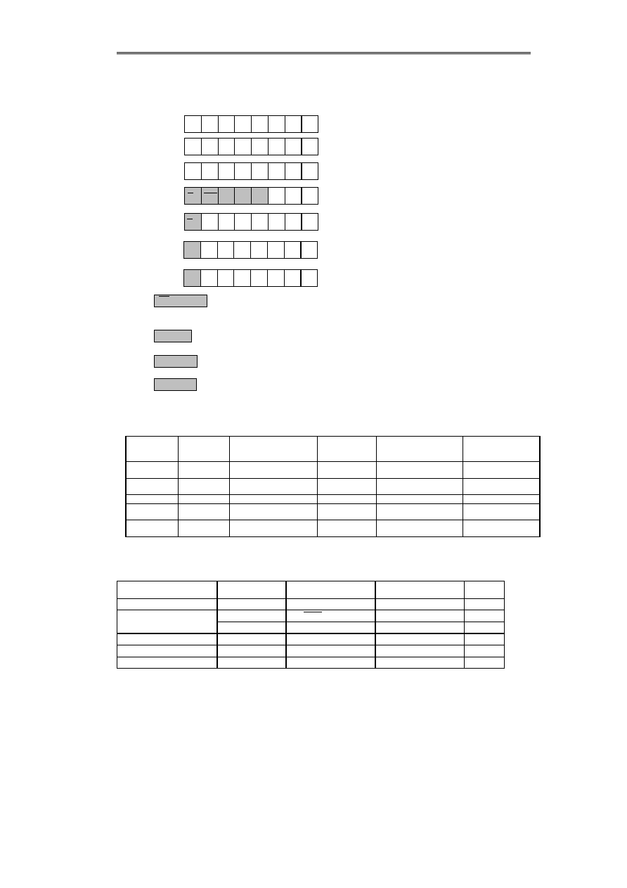
12/24
Y4
Y5
Y6
Y7
0
0
0
M0
M1
M2
M3
M4
POW
S0
S1
S2
S3
S4
S5
S6
BLD
H0
H1
H2
H3
H4
H5
0
AM/PM
TPF FRE
TPEN
Y3
Y2
Y1
Y0
0
0
D5
D4
D3
D2
D1
D0
W2
W1
W0
m6
m5
m4
m3
m2
m1
m0
Year data (0 to 99)
Month data (1 to 12)
Date data (1 to 31)
Status and day data (1 to 7)
Hour data (0 to 23 or 0 to 11) and flags
Minute data (0 to 59) and flags
Second data (0 to 59) and flags
( * )Notes AM /PM Flag:
When writing in 12-hour display mode, always input 0 for AM and 1 for PM. In 24-hour display
mode, it is unnecessary as both 1 and 0 are ignorged. However, when reading the time in either
display mode0 is read as AM 1 as PM.
BLD Flag:
When a decrease in the voltage is detected, it is set to 1. This is valid during reading; and is
invalid during writing.
POW Flag:
1 is set at the power ON, and cleared through the RESET command. This flag is ingored during
writing.
TEST Flag:
When the test mode is set, it is set to 1. When the bit is 1, ALWAYS USE the TEST END or
RESET command to set to 0. This bit is valid for reading and ignored during writing.
TEST
Ta=25
�
C V
SS
=0 V

REAL-TIME CLOCK
S-3510 Series
4
Seiko Instruments Inc.
Recommended Operating Conditions
Table 5
Parameter
Symbol
Min.
Typ.
Max.
Unit
Power supply voltage
V
DD
1.7
3.0
5.5
V
Operating temperature
Topr
-20
+70
�
C
DC Characteristics
Parameter
Symb.
Conditions
Standard
Unit
Note
Min.
Typ.
Max.
Operating voltage
range
V
DD
Ta=-20
�
C to +70
�
C
1.7
3.0
5.5
V
1
1.2
3.5
�
A
2, 15
2.0
3.5
�
A
2, 16
S-3510ANFJX/ AEFJA
10
30
�
A
3,11
S-3510ACFJX/ ADFJA/AFFJA
30
60
�
A
3,12
I
IHL1
V
IN
=5.5 V
-0.5
0.5
�
A
4
Input leak current
I
IHL2
V
IN
=V
DD
-0.5
0.5
�
A
5
I
ILL
V
IN
=0 V
-0.5
0.5
�
A
6
I
IH2
V
IN
=5.5 V
10
30
�
A
7
I
IH3
V
IN
=0.4 V
30
100
300
�
A
7
V
IH
0.8
�
V
DD
V
V
IL
0.2
�
V
DD
V
I
OL1
V
IN
=0.4 V
200
�
A
8
I
OL2
V
IN
=0.4 V
500
�
A
9
I
OH1
V
IN
=2.6 V
-200
�
A
14
I
OH2
V
IN
=2.6 V
-500
�
A
10
1.8
2.0
2.2
V
Ta=-20
�
C to +70
�
C
1.72
2.3
V
BLD current
consumption
I
BLD
Ta=-20
�
C to +70
�
C
0.3
1.0
�
A
13
Unless otherwise specified,
Ta=25
�
C,V
DD
=3.0 V, X
'
tal resonator: Seiko Instruments Inc.,
DS-VT-200 (R
1
=30 k
, C
L
=6 pF, 32768 Hz)
Note 10 Applied to the SIO of the S-
3510ACFJX, the S-3510ADFJA, the
S-3510AFFJA
Note 11
Communications when SCK=100
kHz
Note 12 Communications when SCK=500
kHz
Note 13 The value of the current which flows
through the voltage detector when it
starts to function
Note 14
Applied to the TPout of the S-
3510AFFJA
Note 15
Applied to the products except the S-
3510AFFJA
Note 16
Applied to the S-3510FFJA
Note 5
Applied to the SIO, SCK of the S-
3510ACFJX, the S-3510ADFJA,
the S-3510AFFJA
Note 6
Applied to the SIO, SCK, CS
Note 7
Applied to the CS
Note 8
Applied to the TP
OUT
Note 9
Applied to the SIO
Note 1
Communications when
SCK=100 kHz
Note 2
No output load,
communication inhibit
Note 3
The current which flows
through the CS is not
included, no output load
Note 4
Applied to the SIO, SCK of
the S-3510ANFJX, the S-
3510AEFJA
Table 6
Power current
consumption
I
DD2
Voltage detection
voltage
V
DET
Input voltage
Input current
I
DD1
CS=0 V
Output current

REAL-TIME CLOCK
S-3510 Series
Seiko Instruments Inc.
5
Oscillation Characteristics
Table 7
Ta=25
�
C, V
DD
=3.0 V, X
'
ftal resonator: Seiko Instruments Inc., DS-VT-200 (R
1
=30 k
, C
L
*=6 pF, 32768 Hz)
Standard
Min.
Typ.
Max.
Oscillation start
voltage
V
STA
Within 10 sec
1.7
5.5
V
Oscillation start
time
T
STA
3.0
S
Frequency
deviation between
ICs
IC
-10
+10
ppm
Frequency voltage
deviation
V
V
DD
=1.7 V to 5.5 V
-3
+3
ppm
/
V
Input capacitance
C
IN1
Applied to X
IN
12
P
F
*1
Input capacitance
C
IN2
Applied to X
IN
8
P
F
*2
Output
capacitance
C
OUT
Applied to X
OUT
12
P
F
*3
* The load capacitance (C
L
) changes depending upon the capacitance of the PCB mounted onto the IC.
ADJUST the load capacitance.
*1 Applied to S-3510ANFJX, S-3510ACFJX, S-3510AEFJA (Internal) .
*2 Applied to S-3510ADFJA, S-3510AFFJA (External) .
*3 Applied to S-3510ANFJX, S-3510ACFJX, S-3510AEFJA, S-3510ADFJA, S-3510AFFJA (Internal) .
Parameter
Conditions
Symbol
Note
Unit

REAL-TIME CLOCK
S-3510 Series
6
Seiko Instruments Inc.
AC Characteristics 1
(S-3510ANFJX, S-3510AEFJA, R
L1
=30 k
, C
L1
=50 pF)
Table 8
Conditions
:
V
DD
=1.7 V to 5.5 V, Ta=-20
�
C to 70
�
C, Interface voltage Vcc=5.0 V
Input: V
IH
=0.8
�
V
DD
, V
IL
=0.2
�
V
DD
, Output: V
OH
=0.8
�
V
CC
, V
OL
=0.2
�
V
CC
Parameter
Symbol
Min.
Typ.
Max.
Unit
Clock pulse width
t
SCK
5
250000
�
s
Setup time prior to the rising of the CS
t
DS
1
�
s
Hold time after the rising of the CS
t
CSH
1
�
s
Input data setup time
t
ISU
1
�
s
Input data hold time
t
IHO
1
�
s
Output data determination time
t
ACC
3.5
�
s
Setup time prior to the falling of the CS
t
CSS
1
�
s
Hold time after the falling of the CS
t
DH
1
�
s
Input rising/falling time
t
R
,
t
F
0.1
�
s
AC Characteristics 2
(S-3510ACFJX, S-3510ADFJA, S-3510AFFJA, C
L1
=50 pF)
Table 9
Conditions : V
DD
=5.0
�
0.5 V, Ta=-20
�
C to 70
�
C
Input: V
IH
=0.8
�
V
DD
, V
IL
=0.2
�
V
DD
, Output: V
OH
=0.8
�
V
DD
, V
OL
=0.2
�
V
DD
Parameter
Symbol
Min.
Typ.
Max.
Unit
Clock pulse width
t
SCK
0.5
250000
�
s
Setup time prior to the rising of the CS
t
DS
0.1
�
s
Hold time after the rising of the CS
t
CSH
0.1
�
s
Input data setup time
t
ISU
0.1
�
s
Input data hold time
t
IHO
0.1
�
s
Output data determination time
t
ACC
0.3
�
s
Setup time prior to the falling of the CS
t
CSS
0.1
�
s
Hold time after the falling of the CS
t
DH
0.1
�
s
Input rising/falling time
t
R
,
t
F
0.05
�
s
AC Characteristics 3
(S-3510ACFJX, S-3510ADFJA, S-3510AFFJA, C
L1
=50 pF)
Table 10
Conditions : V
DD
=3.0
�
0.6 V, Ta=-20
�
C to 70
�
C
Input: V
IH
=0.8
�
V
DD
, V
IL
=0.2
�
V
DD
, Output: V
OH
=0.8
�
V
DD
, V
OL
=0.2
�
V
DD
Parameter
Symbol
Min.
Typ.
Max.
Unit
Clock pulse width
t
SCK
1.0
250000
�
s
Setup time prior to the rising of the CS
t
DS
0.2
�
s
Hold time after the rising of the CS
t
CSH
0.2
�
s
Input data setup time
t
ISU
0.2
�
s
Input data hold time
t
IHO
0.2
�
s
Output data determination time
t
ACC
0.6
�
s
Setup time prior to the falling of the CS
t
CSS
0.2
�
s
Hold time after the falling of the CS
t
DH
0.2
�
s
Input rising/falling time
t
R
,
t
F
0.05
�
s
REAL-TIME CLOCK
S-3510 Series
Seiko Instruments Inc.
7
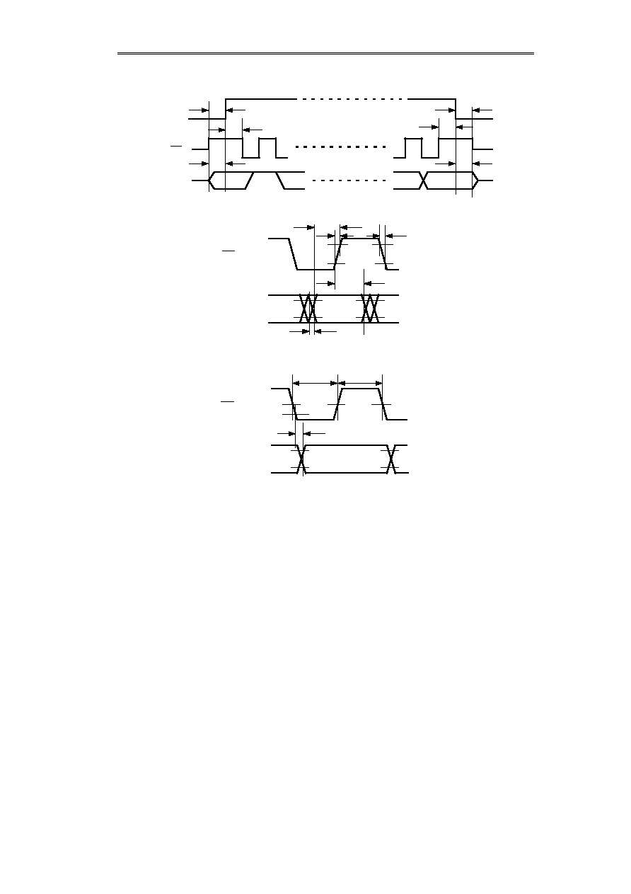
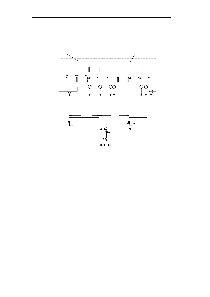
Timing Charts
Figure 5
t
DH
t
DH
t
CSS
t
DS
CS
SCK
SIO
t
DS
t
CSH
80%
80%
20%
20%
50%
20%
80%
20%
20%
80%
t
ACC
t
SCK
t
SCK
t
R
,
t
F
t
F
t
t
ISU
SCK
Input data
t
IHO
50%
SCK
Output data
Figure 3
Figure 4

REAL-TIME CLOCK
S-3510 Series
8
Seiko Instruments Inc.
Operation
(1) Initialization
When the power is switched on, the POW flag is assigned via the power-on detector. ALWAYS TURN the CS to
"
L.
"
Regardless of the logic of the POW flag, initialization must be executed. Therefore, ALWAYS SEND the RESET command
(10101010) from the CPU.
This allows the divider, counter and status register of the S-3510 series to be reset. Namely, the second, minute, hour,
day, date, month, and year (00 sec., 00 min., 00 hr., Sunday (1), January (01), 00 year) are set, and the counter starts to
operate upon the falling edge of the CS.
(2) Write to the Status Register
The S-3510 series is provided with a 4-bit status register. To write the data in the register, send the STATUS WRITE
command (1011D3D2D1D0). This data is retrieved in synchronization with the falling edge of the CS.
Upon initialization, (D3, D2, D1, D0) is set to (1, 0, 1, 0).
In other words,
In the S-3510ANFJX, the S-3510ACFJA, 1 Hz is output from TP
OUT
, and the status is set to the 24-hour display
mode.
In the S-3510AEFJX, the S-3510ADFJA, the S-3510AFFJA, 32768 Hz is output from TP
OUT
, and the status is set to
the 24-hour display mode.
When initialization is not executed, the data of the status register is not specified. ALWAYS execute initialization when
switching on the power.
D1
D2
SIO
CS
SCK
Input
X
1
0
1
0
1
0
1
0
Reset
Figure 6
Free bit:
Stores the information according to a user-specified memory
bit. It does not affect the function of the timer. Reset to
"
0
"
during initialization.
D3
D2
D1
D0
TP
OUT
output frequency-select bit (*)
In the S-3510ANFJA, the S-3510ACFJX
0: 32768 Hz
1: 1 Hz
In the S-3510AEFJA, the S-3510ADFJA, the S-3510AFFJA
0, 1: 32768 Hz (It can be used as Free bit)
TP
OUT
enable bit
In the S-3510ANFJX, the S-3510ACFJX
0: Output
1: High impedance
In the S-3510AEFJA, the S-3510ADFJA, the S-3510AFFJA
0, 1: Output (It can be used as Free bit)
12/24-hour display change bit 0: 12-hour display
1: 24-hour display
(*)
PLEASE NOTE that when the frequency-select bit is rewritten during operation, the first pulse generated immediately after the CS is turned to
"
L
"
cannot be output at the correct frequency.
CS
X
1
0
1
D3
1
D0
SIO
SCK
Figure 7

REAL-TIME CLOCK
S-3510 Series
Seiko Instruments Inc.
9
(3) Data Read
The time data can be read by sending the READ command after the CS goes "H." The data is output in order of the LSB of
the day or year.
After the READ command is interpreted, the time data is transmitted from the counter to the shift register. In
synchronization with the falling edge of the 9th clock, the SIO status changes from input to output, and the LSB of the timer
register is output. After then, in synchronization with the falling edge of the clock, the time data is output from the shift
register.
If the power supply voltage detector activates, the MSB (BLD bit) is set to"1," which allows the power supply voltage to be
monitored. For more details, refer to the "(6) Voltage Detector".
(4) Data Write
Sending the WRITE command after the CS changes from "L" to"H" halts the update operation and resets the frequency
divider. This allows the time data to be written. The data is input in order of the LSB of the day or year. The time data
transmitted from the SIO is written in the shift register in synchronization with the rising edge of the clock. After transmission of
the minute data has been completed, the currently-stored data is transmitted to the counter during the period of the transmission
of the second data, and the month-end correction is executed. The second data is transmitted from the shift register to the
second counter in synchronization with the point where the CS changes from "H" to"L." Accordingly, the second data error
processing is not performed. Turning the CS to "L" allows the divider to run and update operation to start. One second after,
the carry-up signal is transmitted to the second counter. If non-existent data is written in the second counter, the second
counter is set to "00," and the carry-up signal is transmitted to the minute counter.
WWW
0 1 2
m
6
m
5
12
24
m
6
BLD
T
P
E
N
T
P
F
F
R
E
64
9
1
S S S S S S
1 2 3 4 5 6
S
0
P
O
C
Y
7
Y
6
Y
5
Y
4
Y
3
Y
2
Y
1
Y
0
X
X
X
X
0
1
1
1
X
M
0
Output Mode Change
READ1 mode
CS
SCK
SI
READ 2 mode
40
9
1
S S S S S S
1 2 3 4 5 6
S
0
P
O
C
X
X
X
X
1
1
1
1
X
BLD
H
0
m
5
CS
SCK
SIO
T
e
s
t
Figure 8
Output Mode Change

REAL-TIME CLOCK
S-3510 Series
10
Seiko Instruments Inc.
WWW
0 1 2 X
m
6 X
m
5
64
9
1
S S S S S S
1 2 3 4 5 6
S
0
Y
7
Y
6
Y
5
Y
4
Y
3
Y
2
Y
1
Y
0
X
X
X
X
1
0
0
1
X
M
0
WRITE 1 mode
CS
SCK
SIO
X
X
H H H
0 1 2
X X X
m
6
X
WRITE 2 mode
40
9
1
S S S S S S
1 2 3 4 5 6
S
0
X
X
X
X
0
0
0
1
X
m
5
CS
SCK
SIO
X
[Notes]
When the CS is turned to "L,"correct data cannot be written.
NEVER TURN THE CS TO "L" BEFORE WRITE IS COMPLETED. Refer to the timing chart shown below:
Dividing steps are reset at "H."
All bits of the minute, hour and day (date, month, and year) counter are zero cleared at
"H."
With respect to the bit where the data written in the minute, hour and day (date, month,
and year) counter is 1, 1 is set at "H."
Invalid data processing is performed at "H."
Month-end processing is performed at "H."
The second data is written at "H."
S
0
m
6 X
X X X X
8
9
Y
1
Y
0
1
0
0
1
S S S S S
2 3 4 5 6
S
1
CS
SCK
SIO
X
X
Figure 9
Figure 10
REAL-TIME CLOCK
S-3510 Series
Seiko Instruments Inc.
11
(5)
Month-End Correction
When the time data is written in the counter, its validity is checked and either invalid data or month-end processing is
performed.
[Data Processing]
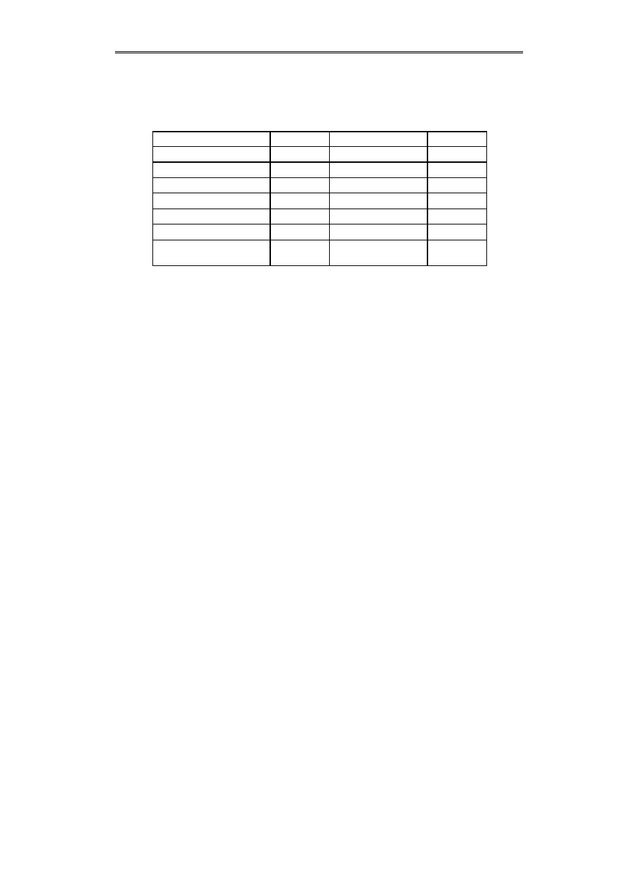
Table 11
Normal data
Error data
Result
Day data
1 to 7
0
1
Date data
01 to 31
00, 32 to 39, XA to XF
01
Month data
01 to 12
00, 13 to 19, XA to XF
01
Year data
00 to 99
XA to XF, AX to FX
00
Second data (*)
00 to 59
60 to 79, XA to XF
00
Minute data
00 to 59
60 to 79, XA to XF
00
Hour data (24-hour)
(**)
(12-hour)
0 to 23
0 to 11
24 to 29, 3X, XA to XF
12 to 19, XA to XF
00
00
(*)
Invalid data processing for the second data is performed through the carry pulse 1 second after
the completion of writing. The carry pulse is sent to the minute counter.
(**)
Write 0 or 1 into the AM/PM flag using the 12-hour display.
For the 24-hour display, 0 or 1 is neglected when writing into the AM/PM flag. When reading,
however, 0 is read during 0 to 11 o
'
clock, and 1 is read during 12 to 23 o
'
clock.
[Month-End Processing]
Non-existent days at the end of the month are automatically processed as the 1st day of the following month. For example,
April 31 is automatically set to May 1. Leap years are allso adjusted.
REAL-TIME CLOCK
S-3510 Series
12
Seiko Instruments Inc.
(6) Voltage Detector
The S-3510 series incorporates a voltage detector that performs sampling once a second for 62.5 msec.
When the supply voltage goes below the detection voltage, the BLD latch-up circuit latches
"
H,
"
and stops sampling.
[IMPORTANT]
The BLD flag can read 1 when the supply voltage increases and the first read is executed. After that, however, sampling is
permitted. Therefore, when the next read is performed after sampling of the detector, the BLD flag is reset. Refer to the
timing charts shown below:
When the CS is turned to "H," the output of the latch-up circuit is transmitted to the shift register only when the subsequent
command is the READ command.
Reading the BLD bit allows the decrease in the voltage to be monitored.
If the CS is turned to "L" after completing the read, sampling restarts. That is, once a decrease in the voltage is detected,
detection is not performed and the status is kept "H" as long as an initialization is not performed or a READ command is not
sent.
Sampling
pulse
Carry pulse
(0)
1 sec
1 sec
Halt
Halt
(1)
(1)
(1) (1)
(1) (1)
(0)
V
CC
CS
Latch circuit output
BLD flag
[Timing of Sampling Pulse]
1Hz
V
DET
Sampling
pulse
0.5 sec
0.5 sec
7.8 msec
Carry-up timing
Latch timing
62.5 msec
31.25 msec
31.25 msec
62.5 msec
Latch pulse
Figure 11
Figure 12
Halt
REAL-TIME CLOCK
S-3510 Series
Seiko Instruments Inc.
13
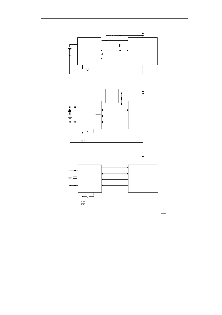
Application Circuit Examples
(1) S-3510ANFJX, S-3510AEFJX (Nch open-drain output)
(2) S-3510ACFJX, S-3510ADFJX (CMOS output)
Vcc
X
OUT
X
IN
S-3510ANFJX/AEFJA
SCK
SIO
TP
OUT
Vss
V
DD
CS
Vss
Vcc
External CPU
Figure 13
S-3510ACFJX/ADFJA
CS
In the case of (2) or (3), the voltage of more than V
DD
cannot be applied to the SIO,CS,SCK. For
communication purpose, switch the system power supply (V
CC
) on, and turn the CS to "H" after the
system power supply stabilizes. ALWAYS TURN THE CS TO "L" AND SWITCH THE SYSTEM
POWER SUPPLY OFF.
X
OUT
X
IN
SCK
SIO
TP
OUT
Vss
V
DD
Vss
Vcc
External CPU
Power
supply
change
circuit
Vcc
Figure 14
*
When V
DD
<V
CC
, the SCK and CS terminals can be directly connected to the CPU because there is no flow of current
from the CPU.
S-3510AFFJA
CS
X
OUT
X
IN
SCK
SIO
TP
OUT
Vss
V
DD
Vss
Vcc
External CPU
Figure 15
(3) S-3510AFFJ (SIO:CMOS output, TPout:CMOS output)
REAL-TIME CLOCK
S-3510 Series
14
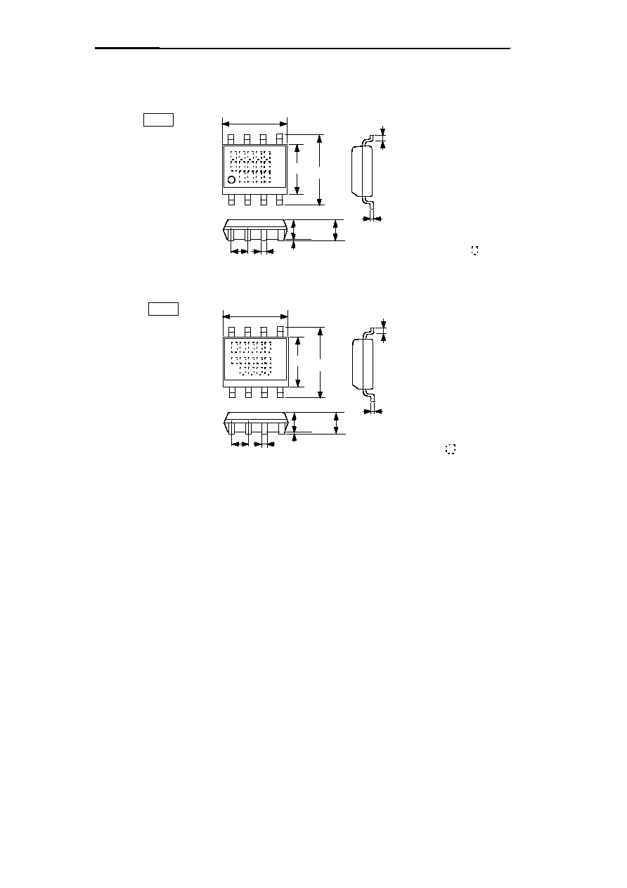
Seiko Instruments Inc.
,
Dimensions
There are two types of packages : A or B.
1.27
0.10 min.
0.40
�
0.05
1.50
�
0.05
1.75max.
3.9
4
5
8
1
4.90 (4.95 max.)
6.00
�
0.20
0.20
�
0.05
0.60
�
0.20
Marking
A type
S-3510ANFJA
S-3510ACFJA
S-3510ADFJA
S-3510AEFJA
S-3510AFFJA
1.27
0.10 min.
0.42
�
0.09
1.47
�
0.05
1.75max.
3.9
4
5
8
1
4.90 (5.00 max.)
6.00
�
0.20
0.22
�
0.03
0.84
Figure 18
Marking
B type
S-3510ANFJ
S-3510ACFJ
REAL-TIME CLOCK
S-3510 Series
Seiko Instruments Inc.
15
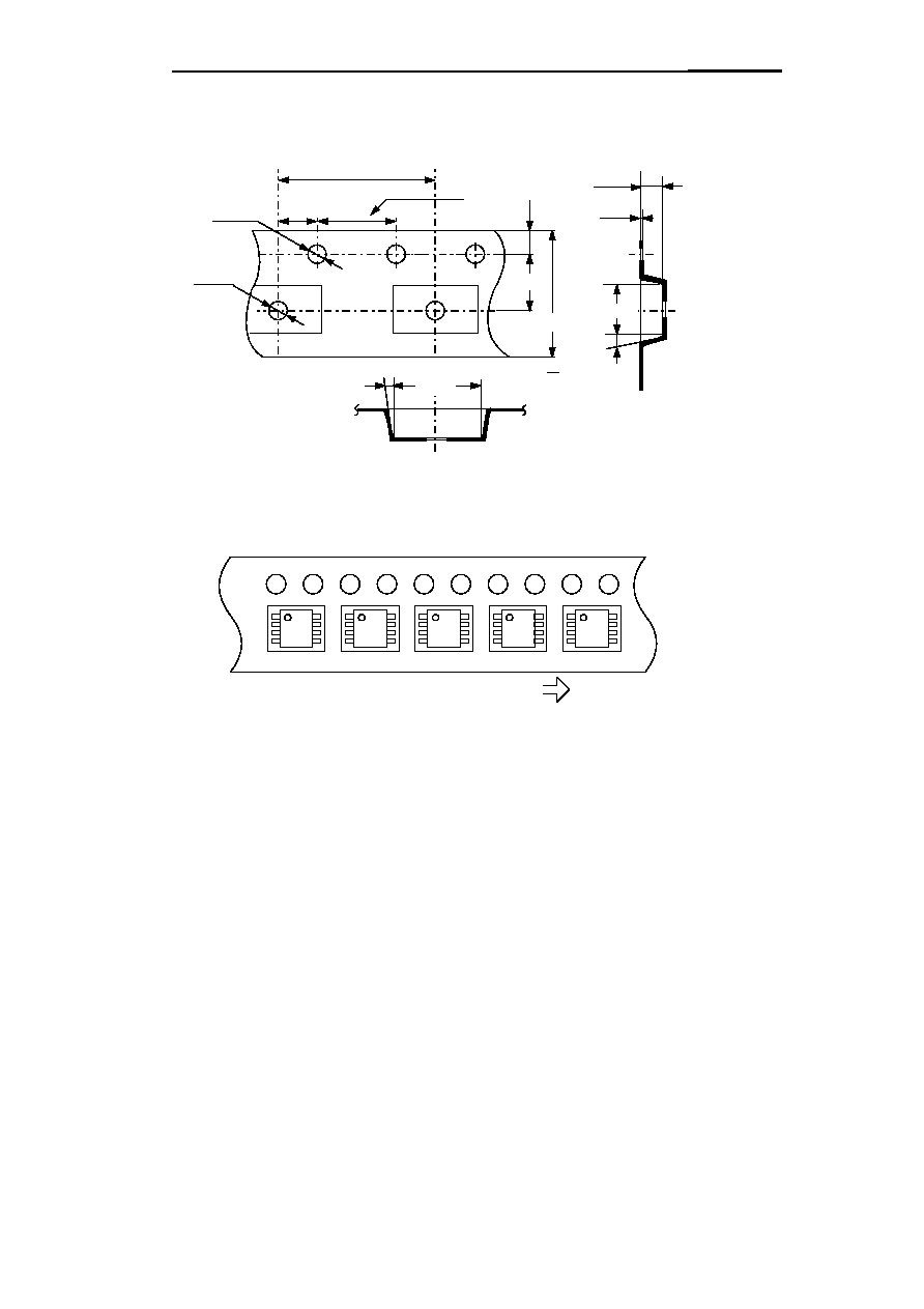
Taping Specifications
(1) Tape Dimensions
(2) Tape Direction
1.75
�
0.1
3
�
or less
0.3
�
0.05
2.1
�
0.1
Total: 10 pitches 40
�
0.2
4.0
�
0.1
2.0
�
0.05
2.00
�
0.05
1.55
�
0.05
Internal dimensions
5.5
�
0.05
12.0
�
0.2
5.50
�
0.1
8.0
�
0.1
5
�
or less
6.7
�
0.1
Unit: mm
[Type TB]
Feed direction

REAL-TIME CLOCK
S-3510 Series
16
Seiko Instruments Inc.
(3) Reel Dimensions (2,000 pcs / 1 reel)
Precautions
(1) The oscillation which uses a quartz crystal resonator is sensitive to external noise which may have an effect on the
accuracy of the watch. MAKE SURE to design your oscillation circuit with this in mind.
A) Configure the quartz crystal resonator as close to the IC as possible.
B) Take measures for sufficient insulation between pins X
IN
and X
OUT
.
C) DO NOT design a circuit where signal lines or the power lines pass close to the oscillation circuit.
(2) When using other resonators, not specified herein or other than the DS- VT-200, ALWAYS check the accuracy and
stability of the oscillation by changing conditions such as the power supply voltage and temperature on the actual
PCB you use.
(3) The load capacitance (C
L
) of the quartz crystal resonator visibly changes depending upon the capacitance of the
PCB mounted onto the IC. Adjust the load capacitance.

REAL-TIME CLOCK
S-3510 Series
Seiko Instruments Inc.
17
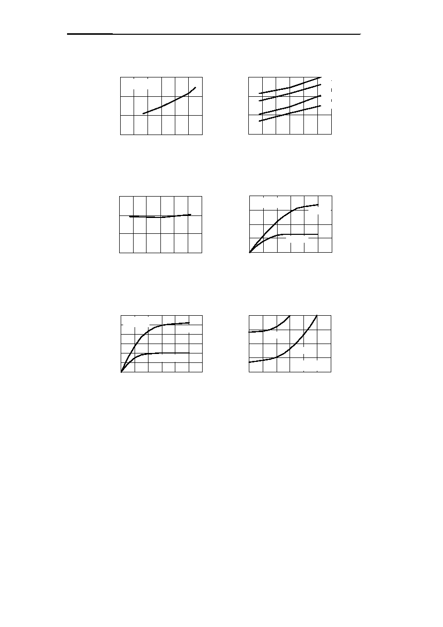
Characteristics
0
1
2
3
4
5
6
0
1
2
3
4
V
DD
(V)
I
DD1
(
�
A)
Ta=25
�
C
1.1 I
DD1
- V
DD
(The products except
the S-3510AFFJA)
0
1
2
3
4
5
6
0
10
25
V
DD
(V)
I
DD2
(
�
A)
SCK=100 kHz
Interface 5 V
Ta=25
�
C
2.1 I
DD2
- V
DD
(S-3510ANFJ
X
, S-3510AEFJA)
-50
0
50
100
0
10
25
I
DD2
(
�
A)
SCK=100 kHz
Interface 5 V
2.2 I
DD2
- Ta
(S-3510ANFJ
X
, S-3510AEFJ
A
)
Ta
(
�
C)
V
DD
=5.0 V
V
DD
=3.0 V
-50
0
50
100
0
20
40
60
I
DD2
(
�
A)
SCK=500 kHz
2.3 I
DD2
- Ta
(S-3510ACFJ
X
, S-3510ADFJA,
S-3510FFJA)
Ta
(
�
C)
V
DD
=5.0 V
V
DD
=3.0 V
0
400
1,000
0
30
60
90
120
I
DD2
(
�
A)
2.4 I
DD2
- f
SCK
(S-3510ACFJ
X
, S-3510ADFJA,
S-3510AFFJA)
f
SCK
( kHz)
V
DD
=5.0 V
V
DD
=3.0 V
1.2 I
DD1
- Ta
Ta
(
�
C)
I
DD1
(
�
A)
-50
0
50
100
0
1
2
3
4
V
DD
=5.0 V
V
DD
=5.5 V
V
DD
=3.0 V
V
DD
=1.7 V
0
1
2
3
4
5
6
0
2
5
V
DD
(V)
I
DD1
(
�
A)
Ta=25
�
C
(S-3510AFFJA)
REAL-TIME CLOCK
S-3510 Series
18
Seiko Instruments Inc.
0
1
2
3
4
5
6
0
0.2
0.4
0.6
V
DD
(V)
I
BLD
(
�
A)
Ta=25
�
C
3.1 I
BLD
- V
DD
Ta
(
�
C)
I
BLD
(
�
A)
3.2 I
BLD
- Ta
-50
0
50
100
1.6
1.8
2
2.2
V
DET
(V)
3.3 BLD detection voltage temperature
characteristics
0
1
2
3
4
5
6
0
1
2
3
4
I
OL1
(mA)
4.1 TP
out
pin output transistor
characteristics
TP
out
pin voltage (V)
V
DD
=5.0 V
V
DD
=3.0 V
0
1
2
3
4
5
6
0
2
4
6
I
OL2
(mA)
4.2 SIO pin output transistor
characteristics
V
DD
=5.0 V
V
DD
=3.0 V
0
1
2
3
4
5
6
-8
-6
-4
-2
0
I
OH2
(mA)
4.3 SIO pin output transistor
characteristics
V
DD
=5.0 V
V
DD
=3.0 V
-50
0
50
100
0
0.2
0.4
0.6
V
DD
=5.0 V
V
DD
=5.5 V
V
DD
=3.0 V
V
DD
=1.7 V
Ta
(
�
C)
SIO pin voltage (V)
Ta=25
�
C
Ta=25
�
C
SIO pin voltage (V)
Ta=25
�
C
Nch
Nch
Pch
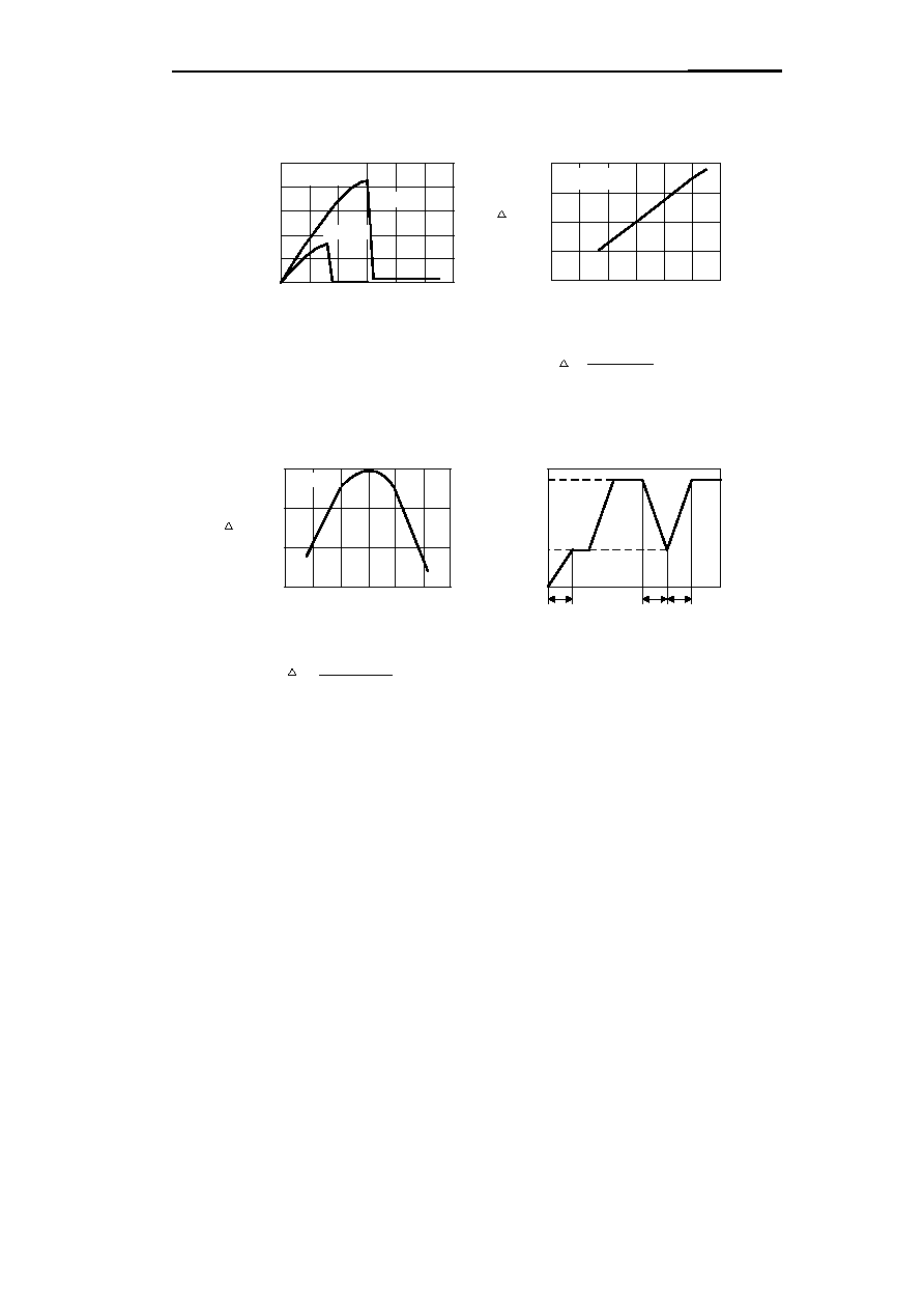
REAL-TIME CLOCK
S-3510 Series
Seiko Instruments Inc.
19
f
Ta
=
f
V
=
t
3
t
2
t
1
f( V
DD
) - f(3 V)
f(3 V)
0
1
2
3
4
5
6
0
0.4
1
CS pin voltage (V)
I
IH
(mA)
Ta=25
�
C
5.1 CS pin input current characteristics
V
DD
(V)
f
V
(ppm)
6.1 Oscillation frequency voltage deviation
6.2 Oscillation frequency temperature deviation
V
DD
(V)
7.1 Power-on detector characteristics
0
1
2
3
4
5
6
-4
-2
0
2
4
Ta
(
�
C)
V
DD
=5.0 V
V
DD
=3.0 V
Ta=25
�
C
�
10
6
(ppm)
f
Ta
(ppm)
f (Ta) - f(25
�
C)
f (25
�
C)
�
10
6
(ppm)
t
1
= Condition where power-on is detected:
t
1
10ms.
t
2
= Condition where the data is retained and
the IC functions normally when the
power supply voltage falls:
t
2
1ms.
t
3
= Condition where the data is retained and
the IC functions normally when the
power supply voltage rises:
t
3
1ms.
5.5
1.7
Ta= - 20
�
C to+70
�
C
10
50
0
-50
-120
-80
-40
0
V
DD
=3.0 V

20
Collection of Product FAQs
Author: Shirai Masaaki
Date: 99/04/16 (Friday) 18:20 (modified: 99/04/16(Friday))
<Information level>
A:
Public (Printing O.K.)
Index:
B: General
<Product>
Division name: 01 IC
Category 1:
17 ASSP
Category 2:
2. Real-Time Clock
Product name: Overall
Related documents:
Question:
What are the notes for time settings (S3511/S3530/S3531)?
Answer:
If time data is rewritten in a product with an alarm interrupt (S-3511/S-3530/S-3531), be sure to disable
the alarm interrupt before the time is set.
Reason: When data is written using real-time data access 2, registers for hours, minutes, and seconds
are reset (all "0"'s), and arbitrary hours, minutes, and seconds are then set. If the alarm is set for 0:00
a.m. and the alarm interrupt is enabled, when the time data is rewritten the registers are reset (all "0"'s)
to 0:00 a.m., the set alarm time, thereby causing an interrupt (INT).
<Remarks>
FAQ No.: 17S35004

21
Collection of Product FAQs
Author: Shirai Masaaki
Date: 99/04/14 (Wednesday) 11:34 (modified: 99/05/18)
<Information level>
A:
Public (Printing O.K.)
Index:
B: Technical
<Product>
Division name: 01 IC
Category 1:
17 ASSP
Category 2:
2. Real-Time Clock
Cal No.:
Overall
Related documents:
Question:
What about the write/read errors (notes)?
Answer:
To continuously write or read data in a 3-wire RTC (S-3511/S-3513/S-35L12/S-3510), be sure to change
"CS" to "L" after the first command has been executed and before the next command is executed. If
commands are continuously executed without changing "CS" to "L," the second command is
disregarded.
Be sure to change
"CS" to "L."
CS
SCK
0
1
0
0
0
1
1
0
X
SIO
Status data
LSB
MSB
Command
MSB
LSB
POWER
9
1
0
1
1
0
0
1
1
0
X
Time data
LSB
MSB
Command
MSB
LSB
<Remarks>
FAQ No.: 17S35003

22
Collection of Product FAQs
Author: Shirai Masaaki
Date: 99/04/13 (Tuesday) 15:40 (modified: 99/05/18)
<Information level>
A:
Public (Printing O.K.)
Index:
A: General
<Product>
Division name: 01 IC
Category 1:
17 ASSP
Category 2:
2. Real-Time Clock
Cal No.:
Overall
Related documents:
Question:
What about the Y2K problem?
Answer:
Our Real-Time Clock outputs information consisting of the last two digits of the year. The S-35L12/L32
can use the register bits in its RTC to determine whether the year is 1900 or 2000 when the last two
digits change from 99 to 00. Most other RTCs, however, cannot determine whether the year is 1900 or
2000 when the last two digits change from 99 to 00. Thus, when this microcomputer is used, the user
must load year information for the RTC in a microcomputer to determine whether the year is 1900 or
2000. Accordingly, when the year reaches 2000, our RTC allows year information to operate normally
and be output as "00," thereby preventing malfunctions.
There is no problem with the operation of the IC. If, however, peripheral circuits and software
developed by a client manage year information using the last two digits of the year, they may
malfunction. Thus, such devices should be checked.
<reference>
http://www.sii.co.jp/sii2000.htm
<Remarks>
FAQ No.: 17S35002

23
Collection of Product FAQs
Author: Shirai Masaaki
Date: 99/04/13 (Tuesday) 14:26 (modified: 99/04/13)
<Information level>
A:
Public (Printing O.K.)
Index:
A: General
<Product>
Division name: 01 IC
Category 1:
17 ASSP
Category 2:
2. Real-Time Clock
Cal No.:
Overall
Related documents:
Question:
Why is an auto calendar available through the year 2099?
Answer:
The SII's RTC denotes the year using its last two digits. These digits are then divided by four, and if
they are divisible the year is determined to be a leap year (the auto calendar determines both 1996 and
2000 to be leap years). The actual calendar, however, does not treat a year with "00" as its last two
digits as a leap year (except for the year 2000; see the following). Accordingly, although 2100 is not a
leap year, the RTC treats it as one. Therefore, this auto calendar is available through 2099.
(Note) A year is defined as a leap year when its last two digits are "00" and its first two digits are
divisible by four.
<Remarks>
FAQ No.: 17S35001