1
SFH6315
SFH6316
SFH6343
HIGH SPEED OPTOCOUPLER
Absolute Maximum Ratings
(continued)
Detector(Si Photodiode + Transistor)
Supply Voltage ............................................................0.5 to 30 V
Output Voltage ..........................................................0.5 to
20 V
Output Current....................................................................... 8 mA
Total Power Dissipation (T
A
70
°
C) ................................... 100 mW
Package
Isolation Test Voltage
between emitter and detector ..............................2500 VAC
RMS
(refer to climate DIN 40046, part 2, Nov. 74)
Pollution Degree (DIN VDE0110) .................................................2
Creepage ............................................................................
4 mm
Clearance............................................................................
4 mm
Comparative Tracking Index
per DIN IEC 112/VDE 0303, part 1 .......................................175
Isolation Resistance
V
IO
=500 V, T
A
=25
°
C, R
ISOL
(Note 2)..............................
10
12
V
IO
=500 V, T
A
=100
°
C, R
ISOL
(Note 2).............................
10
11
Storage Temperature Range .............................. 55
°
C to +150
°
C
Ambient Temperature Range ............................. 55
°
C to +100
°
C
Junction Temperature...........................................................100
°
C
Soldering Temperature (t=10 sec. max.)..............................260
°
C
Dip soldering: distance to seating plane
1.5 mm
Specifications subject to change.
TOLERANCE:
±
.005 (unless otherwise noted)
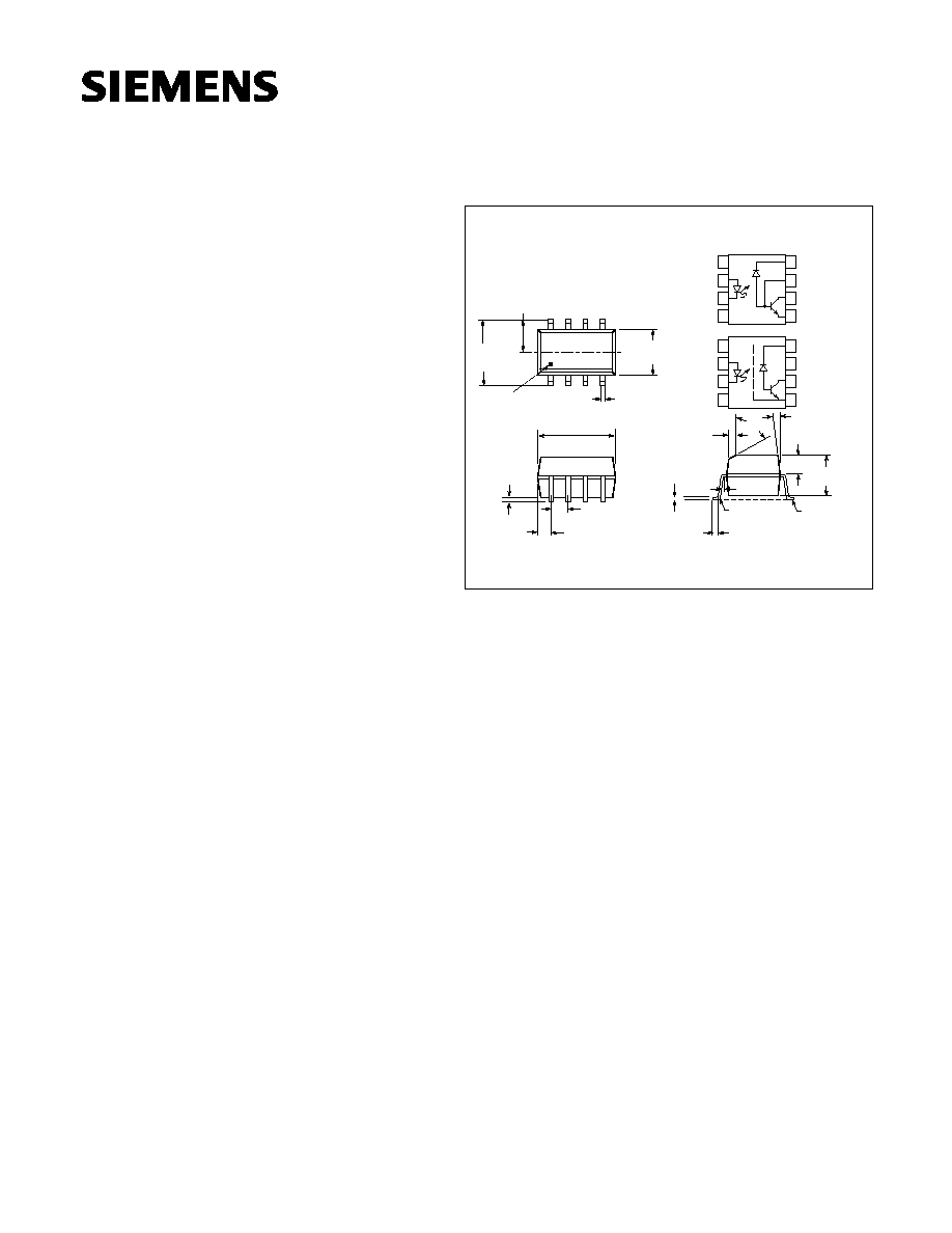
Package Dimensions in Inches (mm)
40
°
Lead
Coplanarity
±
.0015 (.04)
max.
.015
±
.002
(.38
±
.05)
.008 (.20)
7
°
.058
±
.005
(1.49
±
.13)
.125
±
.005
(3.18
±
.13)
.050 (1.27) typ.
.192
±
.005
(4.88
±
.13)
.004 (.10)
.008 (.20)
.021 (.53)
5
°
max.
R.010
(.25) max.
.020
±
.004
(.15
±
.10)
2 plcs.
1
2
3
4
8
7
6
5
V
CC
NC
C
E
NC
A
K
NC
1
2
3
4
8
7
6
5
V
CC
Base V
B
C
E
NC
A
K
NC
SFH6315/6
SFH6343
.240
(6.10)
.154
±
.002
(3.91
±
.05)
.016
(.41)
Pin 1
.120
±
.002
(3.05
±
.05)
CL
FEATURES
·
Surface Mountable
·
Industry Standard SOIC-8 Footprint
·
Compatible with Infrared Vapor Phase Reflow and
Wave Soldering Processes
·
Isolation Voltage, 2500 V
RMS
·
Very High Common Mode Transient Immunity:
15000 V/
µ
s at V
CM
=1500 V Guaranteed (SFH6343)
·
High Speed: 1 Mb/s
·
TTL Compatible
·
Guaranteed AC and DC Performance Over
Temperature: 0
°
C to 70
°
C
·
Open Collector Output
·
Pin Compatible with HP Optocouplers
SFH6315--HCPL0500
SFH6316--HCPL0501
SFH6343--HCPL0453
APPLICATIONS
·
Line Receivers
·
Logic Ground Isolation
·
Analog Signal Ground Isolation
·
Replace Pulse Transformers
DESCRIPTION
The SFH6315/16/43, high speed optocouplers, each
consists of a GaAlAs infrared emitting diode, optically
coupled with an integrated photodetector and a high
speed transistor. The photodetector is junction isolated
from the transistor to reduce miller capacitance effects.
The open collector output function allows circuit design-
ers to adjust the load conditions when interfacing with
different logic systems such as TTL, CMOS, etc.
Because the SFH6343 has a Faraday shield on the
detector chip, it can also reject and minimize high input
to output common mode transient voltages. There is no
base connection, further reducing the potential electrical
noise entering the package.
The SFH6315/16/43 are packaged in industry standard
SOIC-8 packages and are suitable for surface mounting.
Absolute Maximum Ratings
Emitter (GaAlAs)
Reverse Voltage........................................................... 3 V
DC Forward Current................................................25 mA
Surge Forward Current ................................................1 A
tp
1
µ
s, 300 pulses/sec.
Total Power Dissipation (T
A
70
°
C)......................... 45 mW
NE
W

2
SFH6315/6316/6343
Electrical Characteristics
Over recommended temperature (T
A
=0
°
C to 70
°
C) unless otherwise specified. See note 6
. *
All typical values at T
A
=25
°
C.
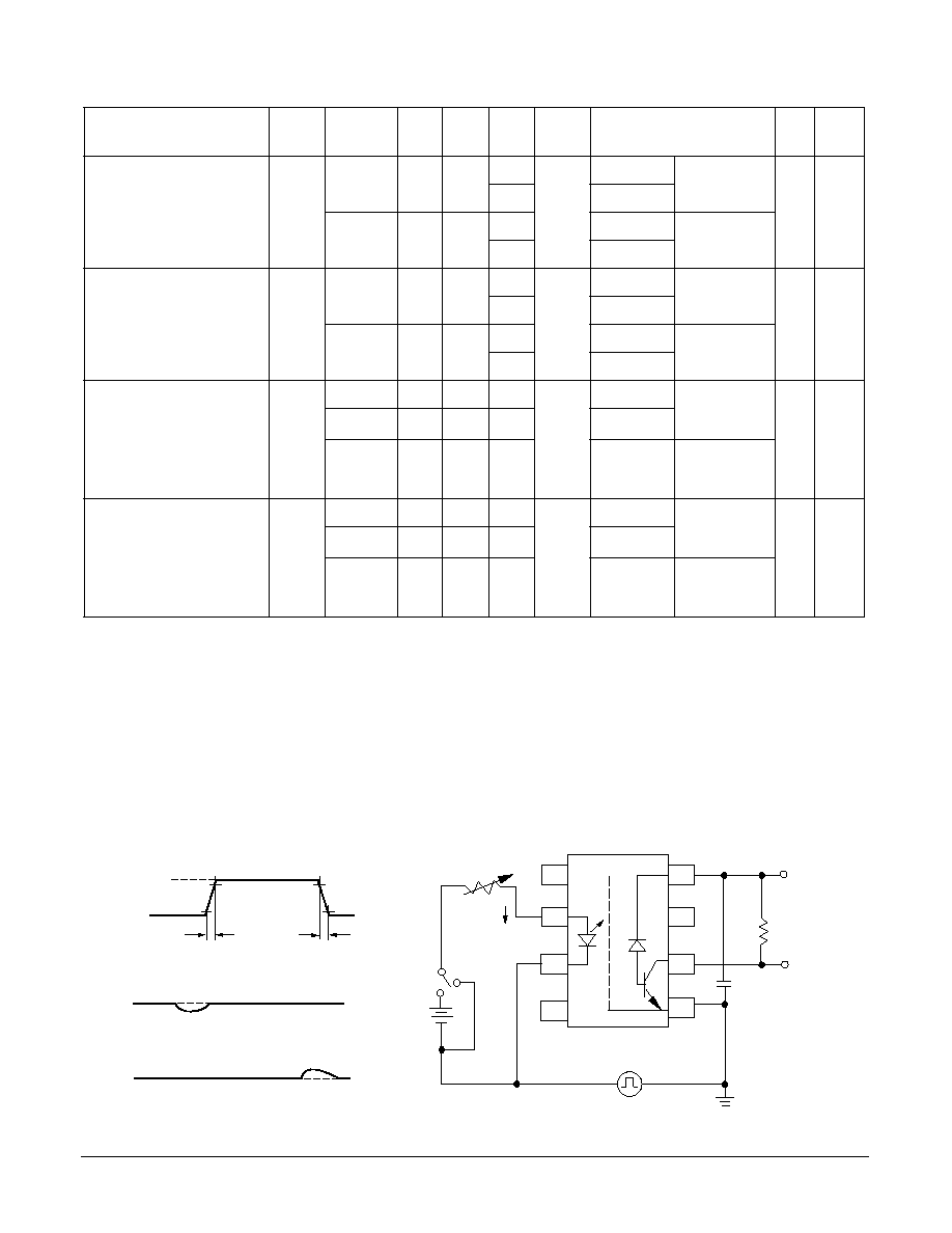
Figure 1. Test circuit for switching times
Parameter
Sym-
bol
Device
Min.
Typ.*
Max.
Units
Test Conditions
Note
Input Forward
Voltage
V
F
1.6
1.8
V
T
A
=25
°
C
I
F
=16 mA
1.9
Input Reverse
Current
I
R
0.5
10
µ
A
V
R
=3 V
Input Capacitance
C
IN
75
pF
f=1 MHz, V
F
=0 V
Temperature
Coefficient of
Forward Voltage
1.7
mV/
°
C
I
F
=16 mA
Logic Low Supply
Current
I
CCL
100
µ
A
I
F
=16 mA, V
O
=Open, V
CC
=15 V
Logic High Supply
Current
I
CCH
0.001
1
µ
A
T
A
=25
°
C
I
F
=0 mA, V
O
=Open, V
CC
=15 V
2
Logic Low Output
Voltage
V
OL
SFH6315
0.15
0.4
V
T
A
=25
°
C
I
O
=1.1 mA
I
F
=16 mA,
V
CC
=4.5 V
0.5
I
O
=0.8 mA
SFH6316
SFH6343
0.15
0.4
V
T
A
=25
°
C
I
O
=3.0 mA
0.5
I
O
=2.4 mA
Logic High Output
Current
I
OH
0.003
0.5
µ
A
T
A
=25
°
C
V
O
=V
CC
=5.5 V
I
F
=0 mA
0.01
1
T
A
=25
°
C
V
O
=V
CC
=15.0 V
50
T
A
=070
°
C
V
O
=V
CC
=15.0 V
Transistor DC
Current Gain
h
FE
150
V
O
=5 V, I
O
=3 mA
Capacitance
(Input-Output)
C
I-O
0.4
pF
f=1 MHz
6
Current Transfer Ra-
tio
CTR
SFH6315
7
16
50
%
T
A
=25
°
C
V
O
=0.4 V
I
F
=16 mA,
V
CC
=4.5 V
1, 6
5
17
V
O
=0.5 V
SFH6316
SFH6343
19
35
50
%
T
A
=25
°
C
V
O
=0.4 V
15
36
V
O
=0.5 V
VF
TA
----------
1
2
3
4
8
7
6
5
5 V
V
O
t
PLH
t
PHL
V
OL
0
I
F
1.5 V
1.5 V
Pulse
Generator
Z
O
=50
tr=5 ns
I
F
=Monitor
10% Duty Cycle
1/f<100
µ
s
I
F
R
L
V
O
C
L
=15pF
0.1
µ
F
+5 V
R
m
3
SFH6315/6316/6343
Switching Specifications
Over recommended temperature (T
A
=0
°
C to 70
°
C), V
CC
=5 V, I
F
=16 mA unless otherwise specified. *All typical values, T
A
=25
°
C
Notes
1.
Current transfer ratio in percent equals the ratio of output collector current (I
O
) to the forward LED input current (I
F
) times 100.
2.
Device considered a two-terminal device: pins 1, 2, 3, and 4 shorted together and pins 5, 6, 7, and 8 shorted together.
3.
Common mode transient immunity in a Logic High level is the maximum tolerable (positive) dV
cm
/dt on the leading edge of the com-
mon mode pulse (V
CM
) to assure that the output will remain in a Logic High state (i.e., V
O
>2.0 V). Common mode transient immunity in
a Logic Low level is the maximum tolerable (negative) dVcm/dt on the trailing edge of the common mode pulse signal (V
CM
to assure
that the output will remain in a Logic Low state (i.e., V
O
<0.8 V).
4.
The 1.9 K
load represents 1 TTL unit load of 1.6 mA and the 5.6 k
pull-up resistor.
5.
The 4.1 K
load represents 1 LSTTL unit load of 0.36 mA and the 6.1 k
pull-up resistor.
6. A
0.1
µ
f bypass capacitor connected between pins 5 and 8 is recommended.
Figure 2. Test circuit for transient immunity and typical waveforms
Parameter
Sym-
bol
Device
Min.
Typ.*
Max.
Units
Test Conditions
Fig.
Note
Propagation Delay Time
to Logic Low at Output
t
PHL
SFH6315
0.5
1.5
µ
s
T
A
=25
°
C
R
L
=4.1 K
1
4, 5
2.0
SFH6316
SFH6343
0.25
0.8
T
A
=25
°
C
R
L
=1.9 K
1.0
Propagation Delay Time
to Logic High at Output
t
PLH
SFH6315
0.5
1.5
µ
s
T
A
=25
°
C
R
L
=4.1 K
1
4, 5
2.0
SFH6316
SFH6343
0.5
0.8
T
A
=25
°
C
R
L
=1.9 K
1.0
Common Mode Transient
Immunity at Logic High Level
Output
|CM
H
|
SFH6315
1
kV/
µ
s
R
L
=4.1 K
I
F
=0 mA
T
A
=25
°
C
V
CM
=10 V
P-P
2
3, 4, 5
SFH6316
1
R
L
=1.9 K
SFH6343
15
30
R
L
=1.9 K
I
F
=0 mA
T
A
=25
°
C
V
CM
=1500 V
P-P
Common Mode Transient
Immunity at Logic Low Level
Output
|CM
L
|
SFH6315
1
kV/
µ
s
R
L
=4.1 K
I
F
=16 mA
T
A
=25
°
C
V
CM
=10 V
P-P
2
3, 4, 5
SFH6316
1
R
L
=1.9 K
SFH6343
15
30
R
L
=1.9 K
I
F
=16 mA
T
A
=25
°
C
V
CM
=1500 V
P-P
V
CM
V
O
5 V
0 V
90%
10%
10%
tr
tf
Switch at A: IF=0 mA
Switch at B: IF=16 mA
90%
V
OL
V
O
1
2
3
4
8
7
6
5
I
F
R
L
V
O
0.1
µ
F
+5 V
V
CM
Pulse Generator
+
V
FF
A
B
4
SFH6315/6316/6343
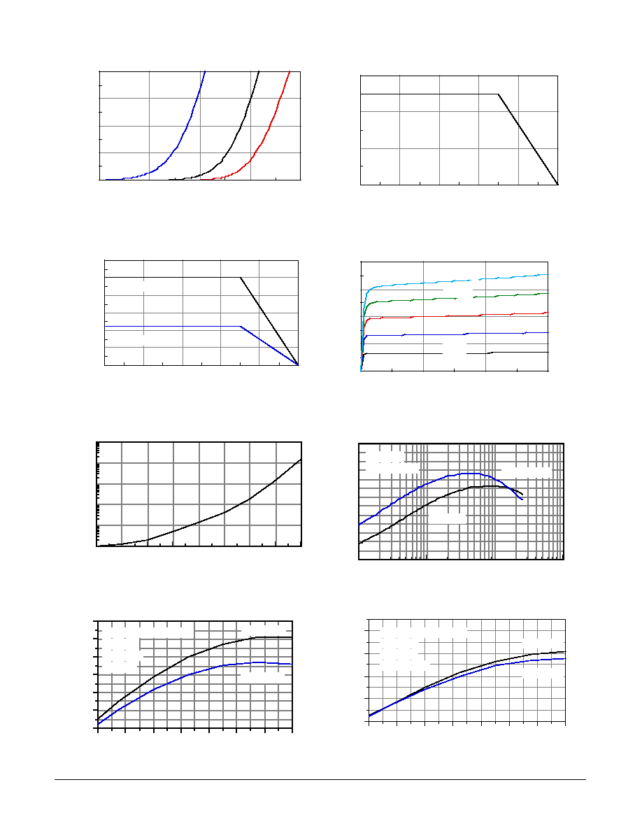
Figure 3. LED forward current vs. forward voltage
Figure 4. Permissible forward LED current vs. temperature
Figure 5. Permissible power dissipation vs. temp.
Figure 6. Output current vs. output voltage
Figure 7. Output current (high) vs. temperature
Figure 8. NCTR vs. IF
Figure 9. NCTR vs. temperature (SFH6316/43)
Figure 10. NCTR vs. temperature (SFH6315)
1.7
1.6
1.5
1.4
1.3
0
5
10
15
20
VF-LED forward Voltage
IF-LED Current in mA
25
°
C
75
°
C
0
°
C
100
80
60
40
20
0
0
10
20
30
Ambient Temperature in
°
C
I
F
LED Current in ma
100
80
60
40
20
0
0
20
40
60
80
100
120
Ambient Temperature in
°
C
Total Power in mW
Detector
Emitter
15
10
5
0
0
2
4
6
8
Vo-Output Voltage in Volts
Io-Output Current in mA
IF=25 mA
20 mA
15 mA
10 mA
5 mA
100
80
60
40
20
0
-20
-40
-60
10 -11
10 -10
10 -9
10 -8
10 -7
10 -6
Ambient Temperature in
°
C
I
o
h
.1
.01
.001
.0001
0.2
0.4
0.6
0.8
1.0
1.2
1.4
IF in mA
NCTR
SFH6315
SFH6316/43
Vcc=5V
Tamb=25
°
C
100
80
60
40
20
0
-20
-40
0.7
0.8
0.9
1.0
1.1
1.2
1.3
Temperature
°
C
NCTR
IF=10 mA
IF=16 mA
Normalized @ 16 mA
Vcc=5v
V0=0.4V
T=25
°
C
100
80
60
40
20
0
-20
-40
0.6
0.8
1.0
1.2
1.4
Temperature in
°
C
NCTR
IF=10 mA
IF=16 mA
Normalized @ 16 mA
Vo=0.4V
VCC=5V
Tamb=25
°
C