
51
FEATURES
· Very High CTR at IF=1 mA, V
CE
=0.5 V
- SFH608-2, 63-125%
- SFH608-3, 100-200%
- SFH608-4, 160-320%
- SFH608-5, 250-500%
· Specified Minimum CTR at I
F
=0.5 mA,
V
CE
=1.5 V:
32% (typ. 120%)
· Good CTR Linearity with Forward Current
· Low CTR Degradation
· High Collector-Emitter Voltage V
CEO
=55 V
· Isolation Test Voltage: 5300 VAC
RMS
· Low Current Input
· Low Coupling Capacitance
· High Common Mode Transient Immunity
· Phototransistor Optocoupler in 6 Pin DIP
Package
· Field Effect Stable: TRIOS*
·
VDE 0884 Available with Option 1
· Underwriters Lab File #E52744
· Applications
- Telecommunications
- Industrial Controls
- Office Machines
- Microprocessor System Interfaces
DESCRIPTION
The SFH 608 is an optocoupler designed for high
current transfer ratio at low input currents with the
output transistor saturated. This makes the device
ideal for low current switching applications. The
SFH608 is packaged in a six pin plastic DIP.
*TRIOS
--
TR
ansparent
IO
n
S
hield
V
D E
Maximum Ratings
(T
A
=25
°
C)
Emitter
Reverse Voltage ...................................................................................6 V
DC Forward Current ........................................................................50 mA
Surge Forward Current (tp
10
µ
s) ................................................... 2.5 A
Total Power Dissipation ................................................................. 70 mW
Detector
Collector-Emitter Voltage .................................................................. 55 V
Collector-Base Voltage .......................................................................55 V
Emitter-Base Voltage ..........................................................................7 V
Collector Current ............................................................................ 50 mA
Surge Collector Current (tp
1 ms) ................................................100 mA
Total Power Dissipation ............................................................... 150 mW
Isolation Test Voltage (between emitter and detector, refer
to climate DIN 40046 part 2 Nov. 74) (t=1 sec.).............. 5300 VAC
RMS
Creepage
.................................................................................................
7 mm
Clearance
.................................................................................................
7 mm
Comparative Tracking Index
per DIN IEC 112/VDE 0303, part1 ................................................... 175
Isolation Resistance
V
IO
=500 V, T
A
=25
°
C
.........................................................................
10
12
V
IO
=500 V, T
A
=100
°
C
.......................................................................
10
11
Storage Temperature Range .......................................... -55
°
C to +150
°
C
Operating Temperature Range....................................... -55
°
C to +100
°
C
Junction Temperature...................................................................... 100
°
C
Soldering Temperature (max. 10 sec., dip soldering:
distance to seating plane
1.5 mm) ............................................. 260
°
C
Dimensions in inches (mm)
.010 (.25)
.014 (.35)
.110 (2.79)
.150 (3.81)
.130 (3.30)
.150 (3.81)
.020 (.051) min.
.300 (7.62)
typ.
.031 (0.80)
.035 (0.90)
.100 (2.54) typ.
.039
(1.00)
Min.
.018 (0.45)
.022 (0.55)
.248 (6.30)
.256 (6.50)
.335 (8.50)
.343 (8.70)
Pin One ID
6
5
4
1
2
3
18
°
typ.
.300 (7.62)
.347 (8.82)
4
°
typ.
1
2
3
6
5
4
Base
Collector
Emitter
Anode
Cathode
NC
SFH 608
PHOTOTRANSISTOR, 5.3 KV, TRIOS
®
LOW CURRENT
OPTOCOUPLER
52
SFH608
Characteristics
(T
A
=25
°
C, unless otherwise specified)
Figure 1. Schematic
I
C
=2 mA (to adjust by I
F
), R
L
=100
, T
A
=25
°
C, V
CC
=5 V
Symbol
Typ
Unit
Condition
Emitter
Forward Voltage
V
F
1.1 (
1.5)
V
I
F
=5 mA
Reverse Voltage
V
R
(
6)
V
I
R
= 10
µ
A
Reverse Current
I
R
0.01 (
10)
µ
A
V
R
=6 V
Capacitance
C
O
25
pF
V
R
=0 V, f=1 MHz
Thermal Resistance
R
thJA
1070
K/W
Detector
Voltage, Collector-Emitter
V
CEO
55
V
I
CE
=10
µ
A
Voltage, Emitter-Base
V
BEO
7
V
I
EB
=10
µ
A
Capacitance
C
CE
10
pF
V
CE
=5 V, f=1 MHz
Capacitance
C
CB
16
pF
V
CE
=5 V, f=1 MHz
Capacitance
C
EB
10
pF
V
CE
=5 V, f=1 MHz
Thermal Resistance
R
thJA
500
K/W
Package
Coupling Capacitance
C
C
0.60
pF
Coupling Transfer Ratio
SFH 608-2
SFH 608-3
SFH 608-4
SFH 608-5
I
C
/I
F
I
C
/I
F
I
C
/I
F
I
C
/I
F
63-125
75 (
32)
100-200
120 (
50)
160-320
200 (
80)
250-500
300 (
125)
%
%
%
%
%
%
%
%
I
F
=1 mA, V
CE
=0.5 V
I
F
=0.5 mA, V
CE
=1.5 V
I
F
=1 mA, V
CE
=0.5 V
I
F
=0.5 mA, V
CE
=1.5 V
I
F
=1 mA, V
CE
=0.5 V
I
F
=0.5 mA, V
CE
=1.5 V
I
F
=1 mA, V
CE
=0.5 V
I
F
=0.5 mA, V
CE
=1.5 V
Saturation Voltage,
Collector-Emitter
SFH 608-2
SFH 608-3
SFH 608-4
SFH 608-5
V
CEsat
V
CEsat
V
CEsat
V
CEsat
0.25 (
0.4)
0.25 (
0.4)
0.25 (
0.4)
0.25 (
0.4)
V
V
V
V
I
C
=0.32 mA, I
F
=1 mA
I
C
= 0.5 mA, I
F
=1 mA
I
C
= 0.8 mA, I
F
=1 mA
I
C
=1.25 mA, I
F
=1 mA
Leakage Current,
Collector-Emitter
I
CEO
10 (
200)
nA
V
CE
=10 V
Description
Symbol
Values
Unit
Turn-On Time
t
ON
8
µ
s
Rise Time
t
R
5
µ
s
Turn-Off Time
t
OFF
7.5
µ
s
Fall Time
t
F
7
µ
s
I
F
47
R
L
I
C
V
CC
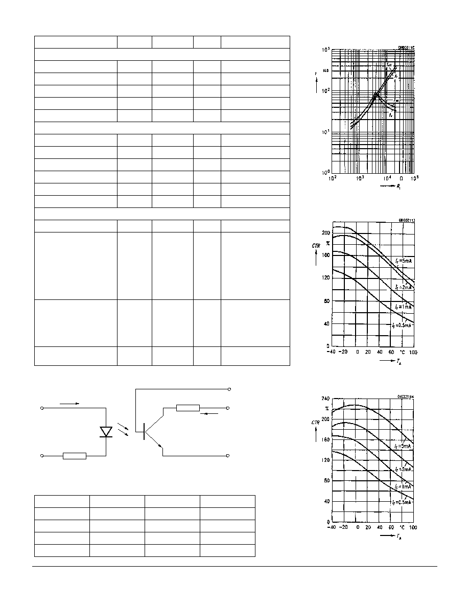
Figure 2. Switching times T
A
=25
°
C,
I
F
=1 mA, V
CC
=5 V, t
ON
, t
R
, t
OFF
, t
F
, =f(R
L
)
Figure 3. Current transfer ratio (typ.)
V
CE
=0.5 V, C
TR
=f(T
A
, I
F
)
Figure 4. Current transfer ratio (typ.)
V
CE
=1.5 V, C
TR
=f(T
A
, I
F
)
53
SFH608
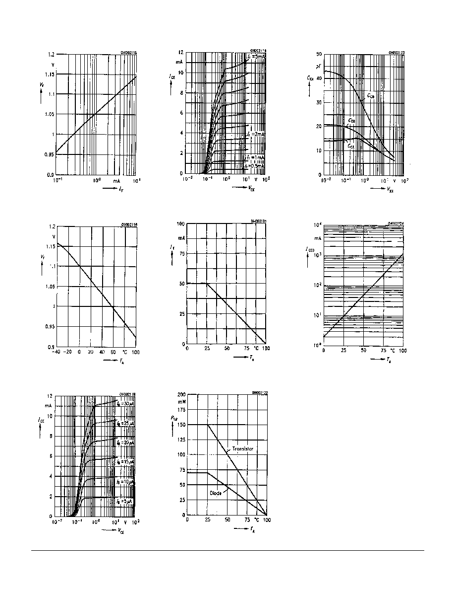
Figure 8. Output characteristics
(typ.) T
A
=25
°
C, I
CE
=f(V
CE
, I
F
)
Figure 9. Permissible forward current
diode I
F
=f(T
A
)
Figure 10. Permissible power dissi-
pation P
TOT
=f(T
A
)
Figure 11. Transistor capacitance
(typ.) T
A
=25
°
C, f=1 MHz, C
CE
=f(V
CE
)
C
CB
=f (V
CB
), C
EB
=f (V
EB
)
Figure 12. Collector-emitter leakage
current I
F
=0, V
CE
=10 V, I
CEO
=f(T
A
)
Figure 5. Diode forward voltage (typ.)
T
A
=25
°
C, V
F
=f(I
F
)
Figure 6. Diode forward voltage (typ.)
I
F
=1 mA, V
F
=f(T
A
)
Figure 7. Output characteristics (typ.)
T
A
=25
°
C, I
CE
=f(V
CE
, I
B
)