
51
FEATURES
· Current Transfer Ratio
IL/ILD/ILQ30/55, 100% min.
IL/ILD/ILQ31, 200% min.
· 125 mA Load Current Rating
· Fast Rise Time, 10
µ
S
· Fast Fall Time, 35
µ
S
· Single, Dual and Quad Channel
· Solid State Reliability
· Standard DIP Packages
· Underwriters Lab File #E52744
·
VDE 0884 Available with Option 1
DESCRIPTION
The IL30/31/55, ILD30/31/55, and ILQ30/31/55 are
optically coupled isolators wih Gallium Arsenide
infrared emitters and silicon photodarlington sen-
sors. Switching can be achieved while maintaining
a high degree of isolation between driving and
load circuits, with no crosstalk between channels.
These optocouplers can be used to replace reed
and mercury relays with advantages of long life,
high speed switching and elimination of magnetic
fields.
The Il30/31/55 are equivalent to MCA230/MCA231/
MCA255. The ILD30/31/55 re designed to reduce
board space requirements in high density applica-
tions.
Maximum Ratings
Emitter
(each channel)
Peak Reverse Voltage........................................ 3 V
Continuous Forward Current......................... 60 mA
Power Dissipation at 25
°
C ......................... 100 mW
Derate Linearly from 25
°
C ................... 1.33 mW/
°
C
Detector
(each channel)
Collector-Emitter Breakdown Voltage
IL/D/Q30....................................................... 30 V
IL/D/Q55....................................................... 55 V
Collector (Load) Current ............................. 125 mA
Power Dissipation at 25
°
C Ambient........... 150 mW
Derate Linearly from 25
°
C ..................... 2.0 mW/
°
C
Package
Total Package Power Dissipation at 25
°
C
IL30/31/55................................................ 250 mW
ILD30/31/55 ............................................. 400 mW
ILQ30/31/55 ............................................. 500 mW
Derate Linearly from 25
°
C
IL30/31/55............................................ 3.3 mW/
°
C
ILD30/31/55 ....................................... 5.33 mW/
°
C
ILQ30/31/55 ....................................... 6.67 mW/
°
C
Isolation Test Voltage ........................ 5300 VAC
RMS
Creepage................................................7 mm min.
Clearance ...............................................7 mm min.
Comparative Tracking Index............................. 175
Storage Temperature ................... 55
°
C to +125
°
C
Operating Temperature................ 55
°
C to +100
°
C
Lead Soldering Time at 260
°
C ....................10 sec.
V
D E
.008 (.20)
.012 (.31)
.130 (3.30)
.150 (3.81)
.130 (3.30)
.150 (3.81)
.280 (7.11)
.330 (8.38)
.020 (.51)
.030 (.76)
.300 (7.62)
typ.
3
°
to 9
°
.0255 (.65)
typ.
.100 (2.54) typ.
.040 (1.02)
.050 (1.27)
.016 (.41)
.020 (.51)
1
2
3
.240 (6.10)
.260 (6.60)
.780 (19.81)
.800 (20.32)
Pin
one
I.D.
14
9
8
.048 (1.22)
.052 (1.32)
.033 (.84)
typ.
16
15
.034 (.86)
6
7
4
5
10
11
12
13
.014
(.35)
typ.
.010 (.25)
.014 (.35)
.110 (2.79)
.150 (3.81)
.130 (3.30)
.150 (3.81)
.020 (.051) min.
.300 (7.62)
typ.
.031 (0.80)
.035 (0.90)
.100 (2.54) typ.
.039
(1.00)
min.
.018 (0.45)
.022 (0.55)
.248 (6.30)
.256 (6.50)
.335 (8.50)
.343 (8.70)
Pin one I.D.
6
5
4
1
2
3
18
°
typ.
.300 (7.62)
.347 (8.82)
4
°
typ.
.255 (6.48)
.268 (6.81)
3
4
6
5
.379 (9.63)
.390 (9.91)
.030 (.76)
.045 (1.14)
4
°
typ.
.100 (2.54) typ.
10
°
typ.
3
°
9
°
.305 typ.
(7.75) typ.
.018 (.46)
.022 (.56)
.008 (.20)
.012 (.30)
.115 (2.92)
.135 (3.43)
1
2
8
7
Pin one I.D.
.130 (3.30
.150 (3.81)
.030 (.76 )
.040 (1.02)
8
7
6
5
Emitter
Collector
Collector
Emitter
Anode
Cathode
Cathode
Anode
1
2
3
4
Emitter
Collector
Collector
Emitter
Emitter
Collector
Collector
Emitter
Anode
Cathode
Cathode
Anode
Anode
Cathode
Cathode
Anode
1
2
3
4
5
6
7
8
16
15
14
13
12
11
10
9
1
2
3
6
5
4
NC
Collector
Emitter
Anode
Cathode
NC
Dimensions in inches (mm)
Quad Channel
Dual Channel
Single Channel
SINGLE CHANNEL
IL30/31/55
DUAL CHANNEL
ILD30/31/55
QUAD CHANNEL
ILQ30/31/55
PHOTODARLINGTON OPTOCOUPLER
52
IL/D/Q30/31/55
Electrical Characteristics
(T
A
=25
°
C)
Symbol
Min.
Typ.
Max..
Unit
Condition
GaAs Emitter (per channel)
Forward Voltage
V
F
1.25
1.5
V
I
F
=20 mA
Reverse Current
I
R
0.1
10
µ
A
V
R
=3.0 V
Capacitance
C
O
25
pF
V
R
=0 V
Detector (per channel)
Collector-Emitter Breakdown Voltage
BV
CEO
30/55
V
I
C
=100
µ
A
Collector-Emitter Leakage Current
I
CEO
1.0
100
nA
V
CE
=10 V, I
F
=0
Collector-Emitter Capacitance
C
CE
3.4
pF
V
CE
=10 V, f=1 MHz
Package
Current Transfer Ratio
IL/D/Q30/55
IL/D/Q31
CTR
100
200
400
400
%
%
I
F
=10 mA,V
CE
=5 V
I
F
=10 mA,V
CE
=5 V
Collector-Emitter Saturation Voltage
V
CEsat
0.9
1.0
V
I
C
=50 mA, I
F
=50 mA
Isolation Test Voltage
5300
VAC
RM
S
Isolation Resistance
R
ISOL
10
12
W
Coupling Capacitance
C
ISOL
0.5
pF
Rise Time
t
R
10
µ
s
V
CC
=13.5 V, I
F
=50 mA,
R
L
=100
Fall Time
t
F
35
µ
s
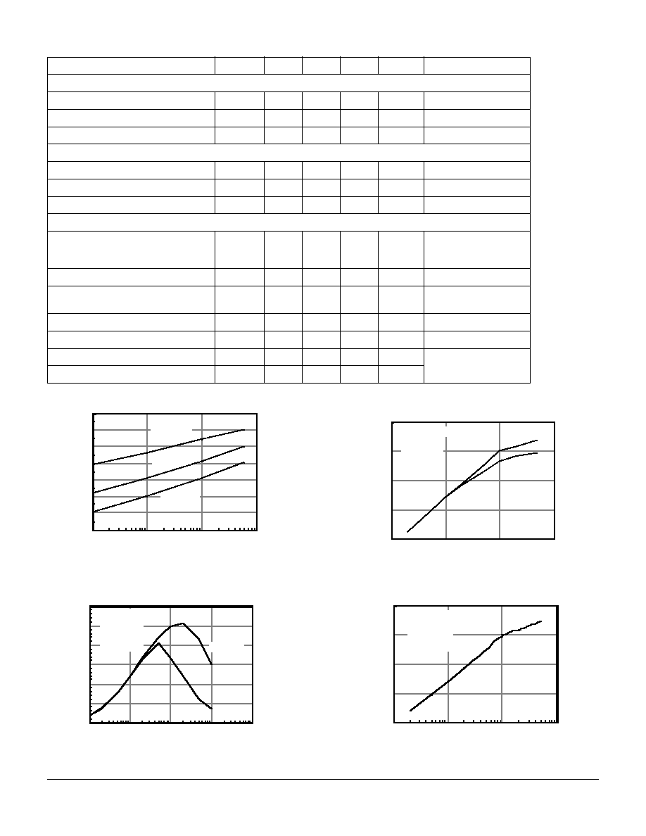
Figure 1. Forward voltage versus forward current
Figure 2. Normalized non-saturated and saturated
CTRce at T
A
=25
°
C versus LED current
100
10
1
.1
0.7
0.8
0.9
1.0
1.1
1.2
1.3
1.4
IF - Forward Current - mA
VF - Forward Voltage - V
Ta = -55
°
C
Ta = 25
°
C
Ta = 85
°
C
.1
1
10
100
1000
0.0
0.2
0.4
0.6
0.8
1.0
1.2
Vce =1V
Vce = 5V
IF - LED Current - mA
NCTRce - Normalized CTR
Vce = 5 V
IF = 10 mA
Ta = 25
°
C
Normalized to:
Figure 3. Normalized non-saturated and saturated
collector-emitter current versus LED current
Figure 4. Normalized collector-base photocurrent
versus LED current
100
10
1
.1
.001
.01
.1
1
10
Vce = 1V
Vce = 5 V
IF - LED Current - mA
NIce - Normalized Ice
Ta = 25
°
C
IF = 10 mA
Vce = 5 V
Normalized to:
.1
1
10
100
.001
.01
.1
1
10
IF - LED Current - mA
NIcb - Normalized Icb
Ta = 25
°
C
Vcb = 3.5 V
IF = 10 mA
Normalized to:
53
IL/D/Q30/31/55
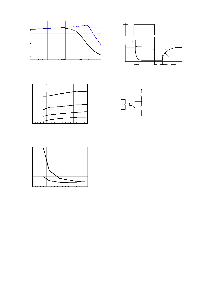
Figure 8. Switching waveforms
Figure 9. Switching schematic
I
F
t
R
V
O
t
D
t
S
t
F
t
PHL
t
PLH
V
TH
=1.5 V
V
O
R
C
V
CC
=13.5 V
F=10 KHz,
DF=50%
IF=50 mA
Figure 5. Hfe current gain versus base current
Figure 6. Low to high propagation delay versus collector
load resistance and LED current
Figure 7. High to low propagation delay versus collector
load resistance and LED current
100
10
1
.1
.01
0
2000
4000
6000
8000
10000
12000
Base Current
Hfe-Current Gain
Vce=5V
Vce=1V
Ta=25
°
C
0
5
10
15
20
0
20
40
60
80
Ta = 25
°
C, Vcc = 5V
Vth = 1.5 V
220
470
1K
g
IF - LED Current - mA
tpLH - Low/High Propagation
Delay -
µ
s
100
0
5
10
15
20
0
5
10
15
20
100
1K
IF - LED Current - mA
tpHL - High/Low Propagation
delay -
µ
s
Ta = 25
°
C
Vcc = 5 V
Vth = 1.5 V