51
FEATURES
· Selected Current Transfer Ratios
20%, 50%, 100% Minimum
· AC or Polarity Insensitive Input
· Built-in Reverse Polarity Input
Protection
· Improved CTR Symmetry
· Industry Standard DIP Package
· Underwriters Lab File #E52744
·
VDE 0884 Available with Option 1
Maximum Ratings
(Per Channel)
Emitter
Continuous Forward Current .........................60 mA
Power Dissipation at 25
°
C..........................100 mW
Derate Linearly from 25
°
C ....................1.33 mW/
°
C
Detector
Collector-Emitter Breakdown Voltage.............. 30 V
Emitter-Base Breakdown Voltage ......................5 V
Collector-Base Breakdown Voltage .................70 V
Power Dissipation at 25
°
C
Single Channel .......................................200 mW
Dual Channel ..........................................150 mW
Derate Linearly from 25
°
C
Single Channel ...................................2.6 mW/
°
C
Dual Channel ......................................2.0 mW/
°
C
Package
Isolation Test Voltage (between
emitter and detector referred to
standard climate 23
°
C/50%RH,
DIN 50014) .................................... 5300 VAC
RMS
Creepage ............................................... 7 mm min.
Clearance............................................... 7 mm min.
Isolation Resistance
V
IO
=500V, T
A
=25
°
C .................................. 10
12
V
IO
=500V, T
A
=100
°
C ................................ 10
11
Total Dissipation at 25
°
C
Single Channel .......................................250 mW
Dual Channel ..........................................400 mW
Derate Linearly from 25
°
C
Single Channel ...................................3.3 mW/
°
C
Dual Channel ......................................5.3 mW/
°
C
Storage Temperature ...................55
°
C to +150
°
C
Operating Temperature ...............55
°
C to +100
°
C
Lead Soldering Time at 260
°
C .................... 10 sec.
V
D E
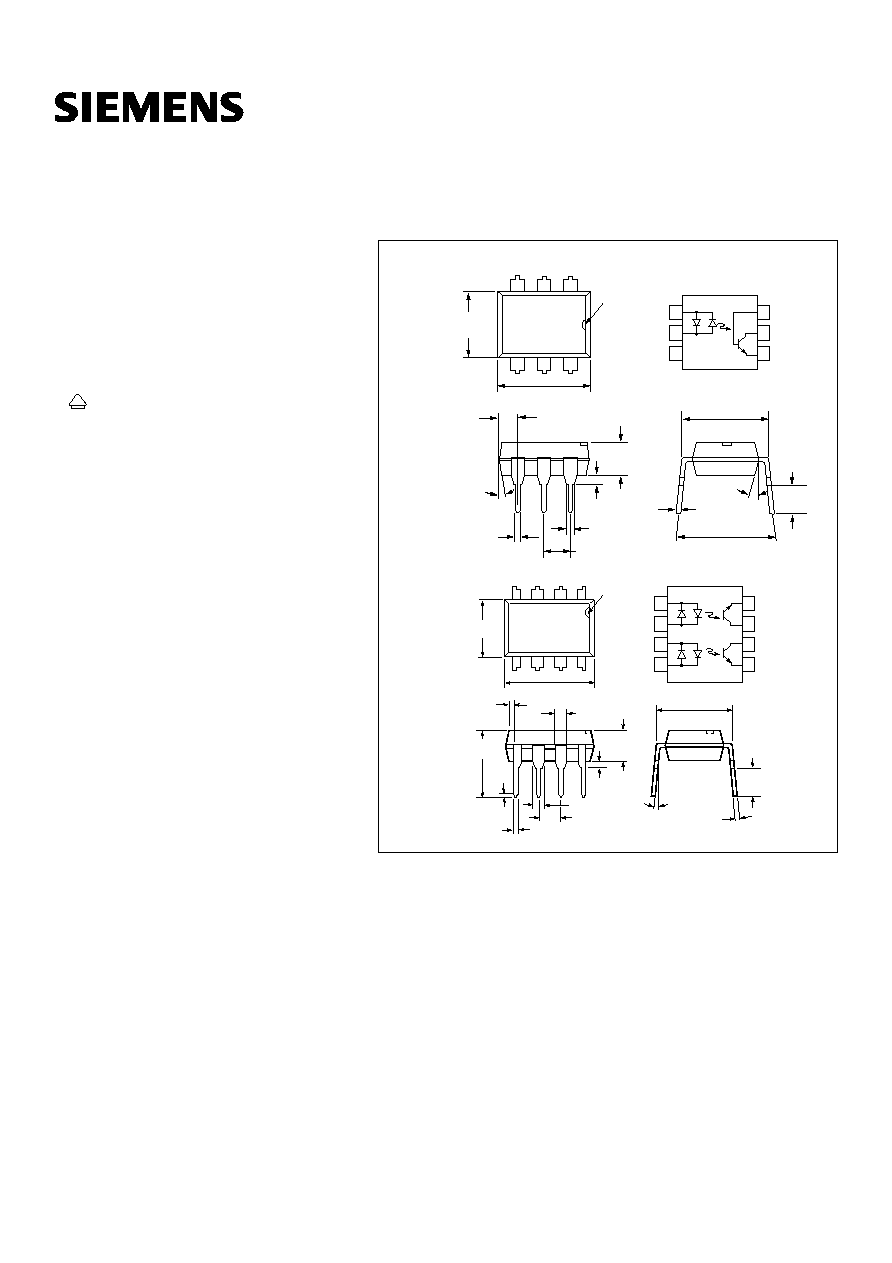
DESCRIPTION
The IL/ILD250/251/252 are bidirectional input optically coupled isolators
consisting of two Gallium Arsenide infrared LEDs coupled to a silicon NPN
phototransistor per channel.
The IL/ILD250 has a minimum CTR of 50%, the IL/ILD251 has a minimum
CTR of 20%, and the IL/ILD252 has a minimum CTR
of 100%.
The IL/IL250/1/2 are single channel optocouplers. The
ILD250/1/2 has two isolated channels in a single DIP package.
These optocouplers are ideal for applications requiring AC signal detection
and monitoring.
Dimensions in inches (mm)
.010 (.25) typ.
.114 (2.90)
.130 (3.30)
.130 (3.30)
.138 (3.50)
.031 (0.80)
.035 (0.90)
.300 (7.62)
typ.
.031 (0.80)
.035 (0.90)
.100 (2.54) typ.
.070 (1.78)
.080 (2.03)
.018 (0.45)
.022 (0.55)
.248 (6.30)
.256 (6.50)
.335 (8.50)
.343 (8.70)
pin one
ID.
6
5
4
1
2
3
18° typ.
.300 (7.62)
.347 (8.82)
4°
typ.
.008 (.20)
.012 (.31)
.130 (3.30)
.150 (3.81)
.130 (3.30)
.150 (3.81)
.280 (7.11)
.330 (8.38)
.020 (.51)
.030 (.76)
.300 (7.62)
typ.
3° to 9°
.033 (.84) typ.
.016(.41)
.020(.51)
1
2
3
0.24 (6.30)
0.260
.388 (9.86)
.400 (10.16)
6
5
4
.048 (1.22)
.052 (1.32)
8
7
.014
(.35)
typ.
.035 (.89)
.040 (1.02)
.100 (2.54) typ.
1
2
3
4
8
7
6
5
Emitter
Collector
Collector
Emitter
Anode/
Cathode
Cathode/
Anode
Anode/
Cathode
Cathode/
Anode
1
2
3
6
5
4
Base
Collector
Emitter
Anode/
Cathode
Cathode/
Anode
NC
Single Channel
Dual Channel
SINGLE CHANNEL
IL250/251/252
DUAL CHANNEL
ILD250/251/252
BIDIRECTIONAL INPUT
OPTOCOUPLER
This document was created with FrameMaker 4.0.4
52
IL250/251/252
Electrical Characteristics
(T
A
=25 C)
Parameter
Min.
Typ.
Max
.
Unit
Condition
Emitter
Forward Voltage V
F
1/2
1.5
V
I
F
=
±
10 mA
Detector
BV
CEO
30
50
V
I
C
=1 mA
BV
EBO
7
10
V
I
E
=100
µ
A
BV
CBO
70
90
V
I
C
=10
µ
A
I
CEO
5
50
nA
V
CE
=10 V
Package
V
CEsat
0.4
V
I
F
=
±
16 mA,
I
C
=2 mA
DC Current Trans-
fer Ratio
%
I
F
=
±
10 mA,
V
CE
=10 V
IL/D250
50
IL/D251
20
IL/D252
100
Symmetry
CTR @ +10 mA
CTR @ - 10 mA
0.50
1.0
2.0
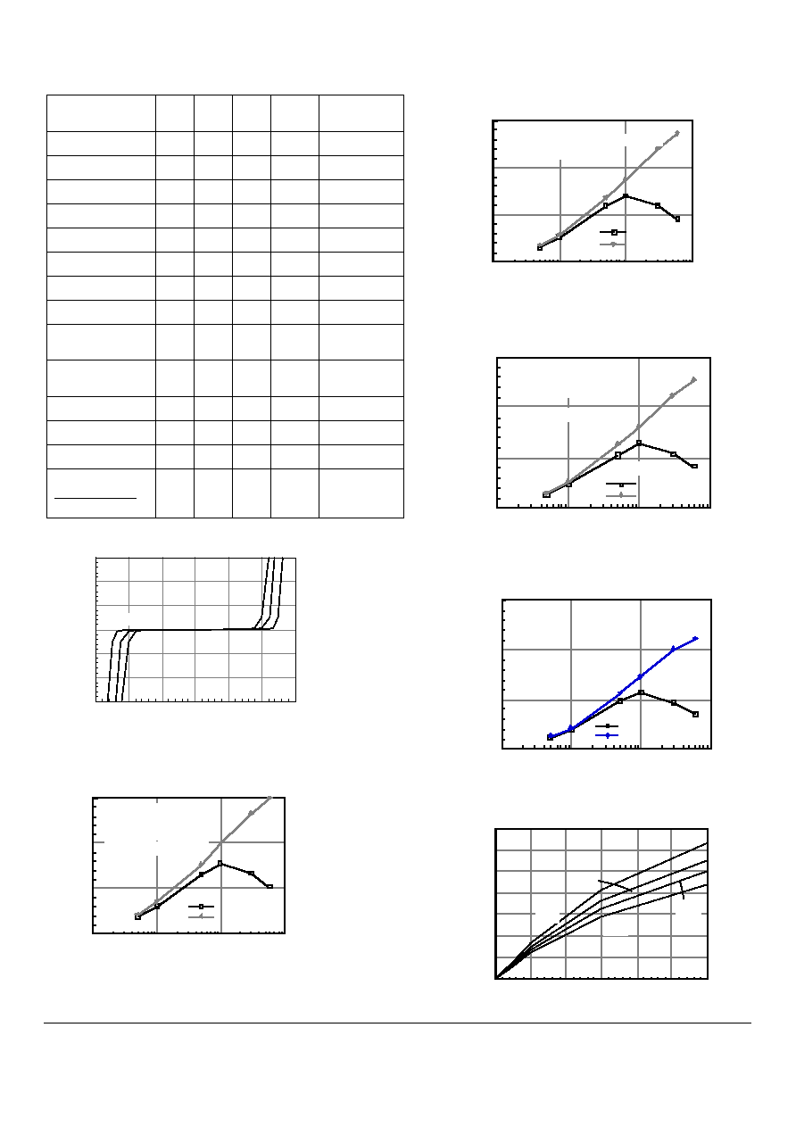
Figure 3. Normalized non-saturated and saturated
CTR at T
A
= 50
°
C versus LED current
Figure 4. Normalized non-saturated and saturated
CTR at T
A
= 70
°
C versus LED current
Figure 5. Normalized non-saturated and saturated
CTR at T
A
= 85
°
C versus LED current
Figure 6. Collector-emitter current versus tempera-
ture and LED current
100
10
1
.1
0.0
0.5
1.0
1.5
NCTR(SAT)
NCTR
IF - LED Current - mA
Normalized to:
Vce = 10V, IF = 10mA, Ta = 25
°
C
Ta = 50
°
C
CTRce(sat) Vce = 0.4V
N
C
T
R
-
N
o
r
m
al
i
z
ed
C
T
R
100
10
1
.1
0.0
0.5
1.0
1.5
NCTR(SAT)
NCTR
IF - LED Current - mA
NCTR - Normalized CTR
Vce = 10V, IF = 10mA
Ta = 25
°
C
Ta = 70
°
C
CTRce(sat) Vce = 0.4V
Normalized to:
100
10
1
.1
0.0
0.5
1.0
1.5
NCTR(SAT)
NCTR
Normalized to:
Vce = 10V, IF = 10mA, Ta = 25
°
C
Ta = 85
°
C
CTRce(sat) Vce = 0.4V
IF - LED Current - mA
NCTR - Normalized CTR
60
50
40
30
20
10
0
0
5
10
15
20
25
30
35
50
°
C
70
°
C
85
°
C
IF - LED Current - mA
Ice - Collector Current - mA
25
°
C
Figure 1. LED forward current versus forward voltage
Figure 2. Normalized non-saturated and saturated
CTR at T
A
= 25
°
C versus LED currenth
-1.5
-1.0
-0.5
0.0
0.5
1.0
1.5
-60
-40
-20
0
20
40
60
25
°
C
-55
°
C
85
°
C
VF - LED Forward Voltage - V
IF - LED Forward Current - mA
100
1 0
1
.1
0.0
0.5
1.0
1.5
NCTR(SAT)
NCTR
IF - LED Curre nt - mA
Normalized to:
Vce = 1 0V, IF = 10m A
Ta = 2 5
°
C
CTRce(sat) Vce = 0.4V
N
C
T
R
-
N
o
r
m
a
liz
e
d
C
T
R

53
IL250/251/252
Figure 11. Normalized non-saturated HFE versus
base current and temperature
Figure 12. Normalized saturated HFE versus base
current and temperature
Figure 13. . Propagation delay versus collector load
resistor
1
10
100
1000
0.4
0.6
0.8
1.0
1.2
Ib - Base Curren t -
µ
A
NHF
E
-
No
r
m
a
l
i
z
e
d
HF
E
Ib = 20
µ
A
Vce = 10 V
Ta = 25
°
C
-20
°
C
25
°
C
50
°
C
70
°
C
Normalized to:
1
10
100
1000
0.0
0.5
1.0
1.5
I b - Base Current -
µ
A
N
H
F
E
(
s
a
t) - N
o
r
m
a
l
i
z
e
d
S
a
tu
r
a
te
d
H
F
E
-20
°
C
25
°
C
50
°
C
70
°
C
Normalized to:
Vce = 10V
Ib = 20
µ
A
Ta = 25
°
C
Vce = 0.4V
100
10
1
.1
1
10
100
1000
1.0
1.5
2.0
2.5
RL - Collector Load Resistor - K
tpLH - Propagation Delay -
µ
s
tpHL - Propagation Delay -
µ
s
tpLH
tpHL
Ta = 25
°
C, IF = 10mA
Vcc = 5 V, Vth = 1.5 V
Figure 7. Collector-emitter leakage current versus
temperature
Figure 8. Normalized CTRcb versus LED current and
temperature
Figure 9. Collector base photocurrent versus LED
current
Figure 10. Normalized photocurrent versus lf and
temperature
100
80
60
40
20
0
-20
10
10
10
10
10
10
10
10
-2
-1
0
1
2
3
4
5
g
p
Ta - Ambient Temperature -
°
C
Iceo - Collector-Emitter - nA
TYPICAL
Vce = 10V
.1
1
10
100
0.0
0.5
1.0
1.5
25
°
C
50
°
C
70
°
C
IF - LED Current - mA
NCTRcb - Normalized CTRcb
Normalized to:
IF =10 mA
Vcb = 9.3 V
Ta = 25
°
C
100
10
1
.1
.01
.1
1
10
100
1000
IF - LED Current - mA
Icb - Collector Base
Photocurrent -
µ
A
Icb = 1.0357 *IF ^1.3631
Ta = 25
°
C
10
100
10
1
.1
.01
.1
1
NIB-Ta=-20
°
C
NIb,Ta=25
°
C
NIb,Ta=50
°
C
NIb,Ta=70
°
C
If - LED Current - mA
N
o
r
m
a
l
i
z
e
d
P
h
o
t
oc
ur
r
e
nt
Normalized to:
If = 10ma, Ta = 25
°
C
Figure 14. Switching timing and schematic
I
F
t
R
V
O
t
D
t
S
t
F
t
PHL
t
PLH
V
TH
=1.5 V
V
O
V
CC
=5 V
R
L
IF=10 mA
F=10 KHz,
DF=50%