51
FEATURES
· Two Channel Optocoupler
· High Current Transfer Ratio at I
F
=1 mA,
500% Min.
· Isolation Test Voltage, 2500 VRMS
· Electrical Specifications Similar to Standard
6-pin Coupler
· Compatible with Dual Wave, Vapor Phase and
IR Reflow Soldering
· Industry Standard SOIC-8 Surface Mountable
Package
· Standard Lead Spacing, .05"
· Available in Tape and Reel Option (Conforms
to EIA Standard 481-2)
· Underwriters Lab File #E52744
DESCRIPTION
The ILD223 is a high current transfer ratio (CTR)
optocoupler. It has a Gallium Arsenide infrared LED
emitter and a silicon NPN photodarlington transis-
tor detector.
This device has CTRs tested at an LED current of
1 mA. This low drive current permits easy interfac-
ing from CMOS to LSTTL or TTL.
The ILD223 is constructed in a standard SOIC-8
foot print which makes it ideally suited for high den-
sity applications. In addition to eliminating through-
holes requirements, this package conforms to stan-
dards for surface mounted devices.
Maximum Ratings
(Each Channel)
Emitter
Peak Reverse Voltage .....................................6.0 V
Peak Pulsed Current (1
µ
s, 300 pps) .................3 A
Continuous Forward Current per Channel ....30 mA
Power Dissipation at 25
°
C............................45 mW
Derate Linearly from 25
°
C ......................0.4 mW/
°
C
Detector
Collector-Emitter Breakdown Voltage...............30 V
Emitter-Collector Breakdown Voltage.................5 V
Power Dissipation per Channel ................... 75 mW
Derate Linearly from 25
°
C ......................3.1 mW/
°
C
Package
Total Package Dissipation at 25
°
C Ambient
(2 LEDs + 2 Detectors, 2 Channels).......240 mW
Derate Linearly from 25
°
C .........................2 mW/
°
C
Storage Temperature ...................55
°
C to +150
°
C
Operating Temperature ............... 55
°
C to +100
°
C
Soldering Time at 260
°
C ............................. 10 sec.
Characteristics
(T
A
=25
°
C)
Symbol
Min.
Typ.
Max.
Unit
Condition
Emitter
Forward Voltage
V
F
1.3
V
I
F
=1 mA
Reverse Current
I
R
0.1
100
µ
A
V
R
=6.0 V
Capacitance
C
O
25
pF
V
F
=0 V,
F=1 MHz
Detector
Breakdown
Voltage
Collector-Emitter
Emitter-Collector
BV
CEO
BV
ECO
30
5
V
V
I
C
=10 mA
I
E
=10 mA
Current,
Collector-Emitter
I
CEO
50
nA
V
CE
=5 V,
I
F
=0
Capacitance,
Collector-Emitter
C
CE
3.4
pF
V
CE
=5 V
Package
DC Current
Transfer Ratio
CTR
DC
500
%
I
F
=1 mA,
V
CE
=5 V
Saturation
Voltage,
Collector-Emitter
V
CEsat
1
V
I
F
=1 mA,
I
CE
=0.5 mA
Capacitance,
Input to Output
C
IO
0.5
pF
Resistance,
Input to Output
R
IO
100
G
Turn-On Time
t
ON
15
µ
s
V
CC
=10 V
R
L
=100
I
F
=5 mA
Turn-Off Time
t
OFF
30
µ
s
Isolation Test
Voltage
V
IO
(t=1 min.)
2500 VAC
RMS
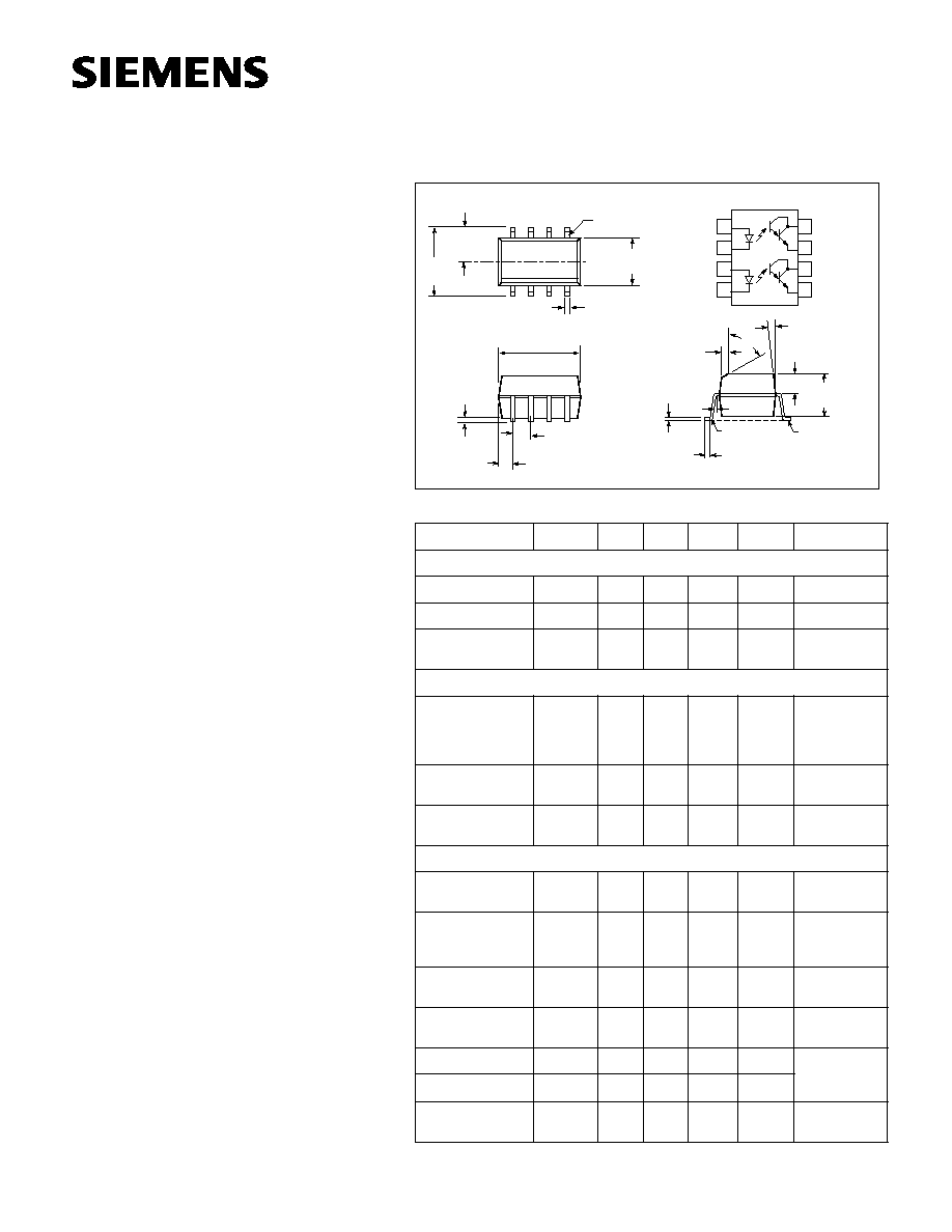
Dimensions in inches (mm)
1
2
3
4
Anode
Cathode
Anode
Cathode
8
7
6
5
Collector
Emitter
Collector
Emitter
40
°
.240
(6.10)
.154
±
.005
(3.91
±
.13)
.050 (1.27) Typ.
.016 (.41)
.192
±
.005
(4.88
±
.13)
.004 (.10)
.008 (.20)
Lead
Coplanarity
±
.001 (.04)
Max.
.015
±
.002
(.38
±
.05)
.008 (.20)
7
°
.058
±
.005
(1.49
±
.13)
.125
±
.005
(3.18
±
.13)
Pin 1
.120
±
.005
(3.05
±
.13)
CL
.040 (1.02)
5
°
Max.
R.010
(.25) Max.
.020
±
.004
(.15
±
.10)
2 Plcs.
ILD223
DUAL PHOTODARLINGTON
SMALL OUTLINE
SURFACE MOUNT OPTOCOUPLER
52
ILD223
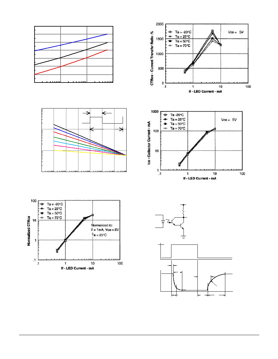
Figure 1. Forward voltage versus forward current
Figure 2. Peak LED current versus duty factor, Tau
Figure 3. Normalized CTR
CE
versus LED current
.1
1
10
100
0.7
0.8
0.9
1.0
1.1
1.2
1.3
1.4
If - Forward Current - mA
Vf-Forward Voltage - V
Ta = -55
°
C
Ta = 25
°
C
Ta = 100
°
C
10-6
10-5
10-4
10-3
10-2
10-1
10 0
10 1
10
100
1000
10000
t - LED Pulse Duration - s
If(pk) - Peak LED Current - mA
.005
.05
.02
.01
.1
.2
.5
Duty Factor
t
DF = /t
Figure 4. CTR versus LED current
Figure 5. Collector current versus LED current
Figure 6. Switching schematic and switching timing
V
O
R
L
V
CC
=10 V
F=10 KHz,
DF=50%
IF=10 mA
I
F
t
R
V
O
t
D
t
S
t
F
t
PHL
t
PLH
V
TH
=1.5 V