51
IL485
OPTICALLY COUPLED
HIGH SPEED MOSFET DRIVERS
OPTOCOUPLER
Maximum Ratings
Emitter
Reverse Voltage ..................................................................................4 V
Forward Current ..............................................................................60 mA
Peak Forward Current....................................................................600 mA
Power Dissipation .........................................................................100 mW
Thermal Resistance....................................................................700
°
C/W
Detector
Breakdown Voltage (pin 5 to 6) ........................................................300 V
Peak Input Current (pin 5 to 4) ........................................................50 mA
Reverse Current (pin 5 to 6, V=100 V) ...........................................200 nA
Power Dissipation (pin 5 to 4) ......................................................150 mW
Package
Insulation Thickness between Emitter and Detector ...................
0.4 mm
Isolation Test Voltage (1 sec.)..............................................5300 VAC
RMS
Isolation Resistance
V
IO
=500 V, T
A
=25
°
C..................................................................
10
12
V
IO
=500 V, T
A
=100
°
C...............................................................
10
11
Comparative Tracking Index per
DIN IEC 112/VDE 303, Part 1.........................................................
175
Total Power Dissipation ................................................................250 mW
Storage Temperature Range ..........................................55
°
C to +150
°
C
Operating Temperature Range.......................................55
°
C to +100
°
C
Junction Temperature ...................................................................... 100
°
C
Soldering Temperature (max. 10 sec.,
dip soldering distance to seating plane >1.5 mm)...................... 260
°
C
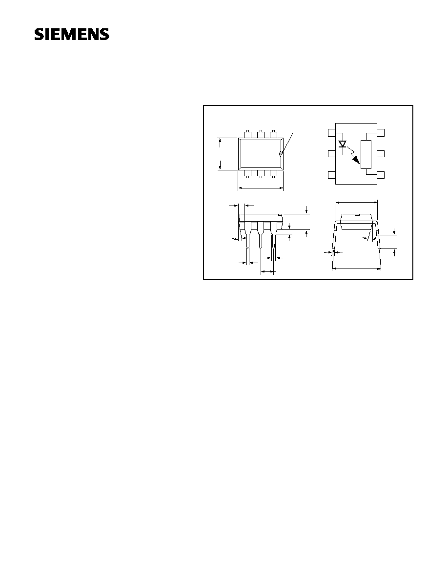
Dimensions in inches (mm)
1
2
3
A
K
4 +out
6 out
5 B
.010 (.25)
.014 (.35)
.110 (2.79)
.150 (3.81)
.130 (3.30)
.150 (3.81)
.020 (.051) Min.
.300 (7.62)
Typ.
.031 (0.80)
.035 (0.90)
.100 (2.54) Typ.
.039
(1.00)
Min.
.018 (0.45)
.022 (0.55)
.248 (6.30)
.256 (6.50)
.335 (8.50)
.343 (8.70)
Pin One ID.
6
5
4
1
2
3
18
°
Typ.
.300 (7.62)
.347 (8.82)
4
°
Typ.
FEATURES
· Fast Turn On
· Fast Turn Off
· Low Input Current
· Isolation Test Voltage, 5300 VAC
RMS
APPLICATIONS
· Motor Drive Controls
· IGBT-predrivers
· AC/DC Power Inverters
DESCRIPTION
The IL485 is a photovoltatic generator (optically cou-
pled) designed to drive highly capacitive loads such
as the gate of a power MOSFET transistor and at the
same time provide isolation and floating voltage sup-
ply capability. The coupler consists of a GaAlAs light
emitting diode as input control and a custom photo IC
chip with photodiode arrary (PDA) as output device.
When the LED is turned on, the emitted light pro-
duces a voltage in the PDA. The output of the PDA is
used to drive the gate of a power MOSFET. The photo
IC chip contains additional circuitry to enhance the
switching speeds, (both turn on turn off). The opto-
coupler is packaged in a 6 pin DIP.

52
IL485
Electrical Characteristics
Parameter
Symbol
Min.
Typ.
Max. Unit
Condition
Input -- Emitter
LED Forward Voltage
V
F
0.9
1.5
2.1
V
I
F
=10 mA
LED Junction Capacitance
C
J
25
pF
V
R
=0 V, f=1 MHz
MOSFET Driver Output with External Biasing (see Figure 1 and Figure 3)
Zener Voltage (pin 4 to 6)
V
Z
13
V
I
ZT
=10
µ
A
Dynamic Output Voltage (pin 4 to 6)
V
OUT
9
11
V
C
L
=2000 pF, V
B
=20 V
I
F
=10 mA
Dynamic Output Current (pin 4 to 6)
I
OUT
5
15
mA
mA
C
L
=2000 pF, V
B
=20 V
I
F
=10 mA
I
F
=40 mA
Dynamic Output Resistance
Sourcing (pin 4)
Sinking (pin 4)
R
OUT
300
20
I
F
=10 mA
Turn-on Time
t
ON
3.5
5
µ
s
C
L
=2000 pF, I
F
=40 mA
Measure at V
OUT
=5 V, V
B
=20 V
Turn-off Time
t
OFF
3.5
5
µ
s
C
L
=2000 pF, I
F
=40 mA
Measure at V
OUT
=2 V, V
B
=20 V
MOSFET Driver Output without External Biasing (see Figure 2 and Figure 3)
Output Open Circuit Voltage (pin 4 to 6)
V
OC
7
10
V
I
F
=10 mA
Output Short Circuit Current (pin 4 to 6)
I
SC
2.1
8.4
4
16
µ
A
µ
A
I
F
=10 mA
I
F
=40 mA
Dynamic Output Resistance Sinking (pin 4)
R
OUT
20
I
F
=10 mA
Turn-on Time
t
ON
650
1000
µ
s
C
L
=2000 pF (see Figure 3)
Measure at V
OUT
=5 V, I
F
=40 mA
Turn-off Time
t
OFF
3
5
µ
s
C
L
=2000 pF (seeFigure 3)
Measure at V
OUT
=2 V, I
F
=40 mA
MOSFET Driver Output Switching Speed (see Figure 3, Figure 4, Figure 5)
Rise time
t
R
500
ns
M1 Cgs=2000 pF, V
S
=50 V
Measure at 90%10% M1 V
DS
(see Figure 4)
Turn-on Time
t
ON
3.5
µ
s
Fall time
t
F
300
ns
Turn-off Time
t
OFF
3.5
µ
s
Package Isolation Characteristics
Input-Output CMRR
dv/dt
15 kV
V/
µ
s
V
CM
=1000 V
Coupling Capacitance
C
IO
1
pF
f=1 MHz

53
IL485
Figure 1. Switching time measurement with external
voltage bias
Figure 2. Switching time measurement
Figure 3. IL485 connected in AC load switching
configuration
Photo
diode
array
1
2
3
4
5
6
C
L
IF
Vo
B
VB
Photo
diode
array
1
2
3
4
5
6
C
L
IF
Vo
B
5V
2V
on
t
off
t
I
LED
Vout
t
t
Figure 4. Switching time measurement without voltage bias
Figure 5. IL485 connected in DC load switching configuration
Photo
diode
array
Load
2N2222
100
1K
2000 pF
300V
+5V
1
2
3
4
5
6
Vs
M1
M1
M2
Photo
diode
array
Load
2N2222
100
1K
2000 pF
300V
+5V
1
2
3
4
5
6
ac
ac