51
FEATURES
· High Current Transfer Ratio
CNY17-1, 40 to 80%
CNY17-2, 63 to 125%
CNY17-3, 100 to 200%
CNY17-4, 160 to 320%
· Breakdown Voltage, 5300 VAC
RMS
· Field-Effect Stable by TRIOS*
· Long Term Stability
· Industry Standard Dual-in-Line Package
· Underwriters Lab File #E52744
·
VDE #0884, Available with Option 1
DESCRIPTION
The CNY17 is an optically coupled pair consisting
of a Gallium Arsenide infrared emitting diode opti-
cally coupled to a silicon NPN phototransistor.
Signal information, including a DC level, can be
transmitted by the device while maintaining a high
degree of electrical isolation between input and out-
put.
The CNY17 can be used to replace relays and
transformers in many digital interface applications,
as well as analog applications such as CRT modu-
lation.
Maximum Ratings
(T
A
=25
°
C)
Emitter
Reverse Voltage .................................................6 V
Forward Current............................................ 60 mA
Surge Current (t
10
µ
s) ................................... 2.5 A
Power Dissipation .......................................100 mW
Detector
Collector-Emitter Breakdown Voltage ...............70 V
Emitter-Base Breakdown Voltage .......................7 V
Collector Current .......................................... 50 mA
Collector Current (t <1 ms)......................... 100 mA
Power Dissipation .......................................150 mW
Package
Isolation Test Voltage (Between emitter &
detector referred to climate DIN 40046,
part 2, Nov. 74) ..............................5300 VAC
RMS
Creepage Distance
..........................................
7 mm
Clearance Distance
.........................................
7 mm
Isolation Thickness between
Emitter and Detector
.................................
0.4 mm
Comparative Tracking Index per DIN IEC 112/
VDE0303, part 1.............................................175
Isolation Resistance
V
IO
=500 V, T
A
=25
°
C
...................................
10
12
V
IO
=500 V, T
A
=100
°
C
................................
10
11
Storage Temperature ................... 55
°
C to +150
°
C
Operating Temperature ............... 55
°
C to +100
°
C
Junction Temperature ....................................100
°
C
Soldering Temperature (max . 10 s, dip soldering:
distance to seating plane
1.5 mm) ..........260
°
C
V
D E
Characteristics
(T
A
=25
°
C)
Symbol
Unit
Condition
Emitter
Forward Voltage
V
F
1.25
(
1.65)
V
I
F
= 60 mA
Breakdown Voltage
V
BR
6
V
I
R
= 10 mA
Reverse Current
I
R
0.01 (
10)
µ
A
V
R
= 6 V
Capacitance
25
pF
V
R
= 0 V, f =1 MHz
Thermal Resistance
R
thjamb
750
K/W
Detector
Capacitance
C
CE
C
CB
C
EB
5.2
6.5
7.5
pF
pF
pF
V
CE
=5 V, f =1 MHz
V
CB
=5 V, f =1 MHz
V
EB
=5 V, f =1 MHz
Thermal Resistance
R
thjamb
500
K/W
Package
Collector-Emitter
Saturation Voltage
V
CEsat
0.25 (
0.4)
V
I
F
=10 mA,
I
C
=2.5 mA
Coupling Capacitance
C
C
0.6
pF
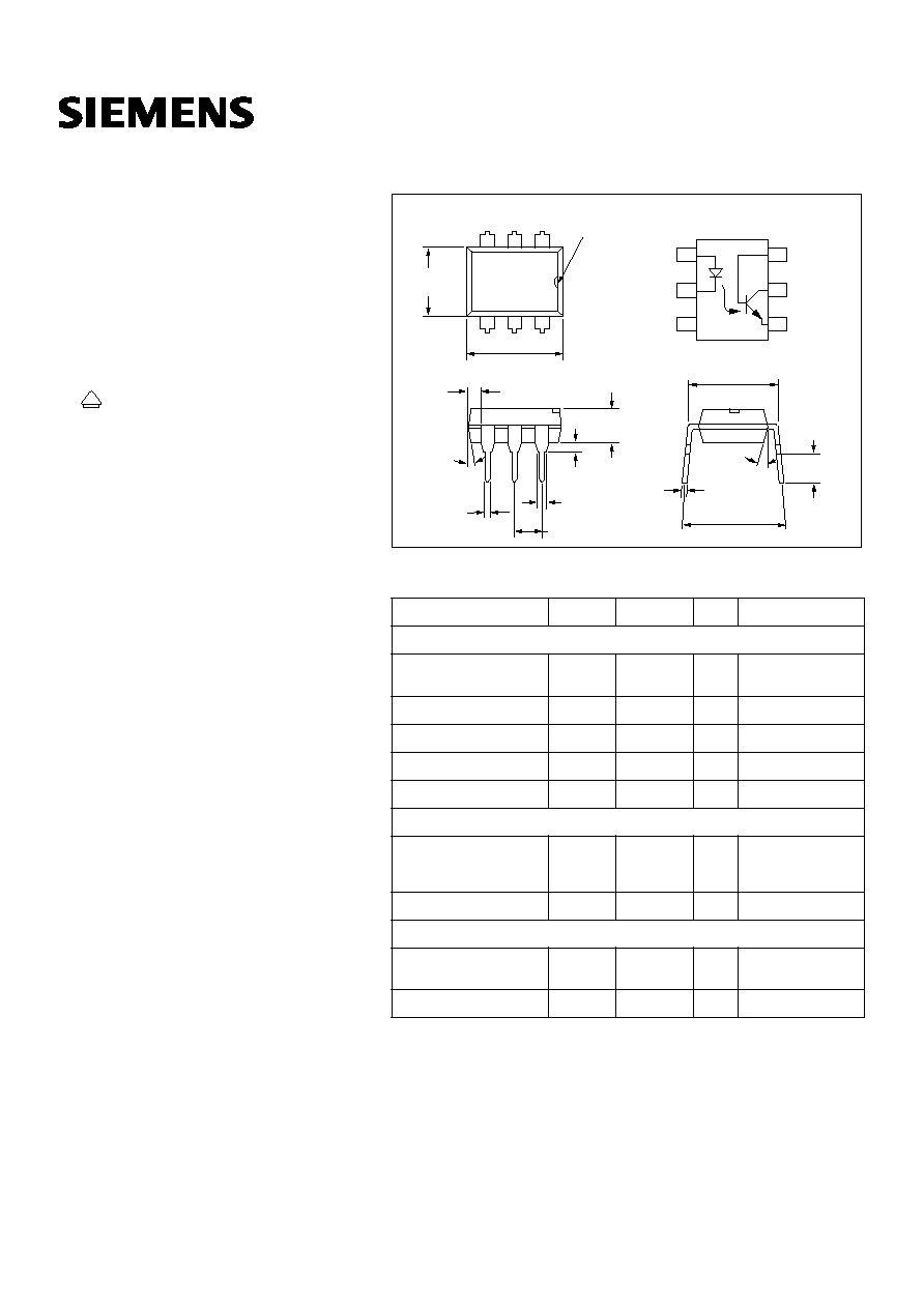
Dimensions in inches (mm)
.010 (.25)
.014 (.35)
.110 (2.79)
.150 (3.81)
.130 (3.30)
.150 (3.81)
.020 (.051) min.
.300 (7.62)
typ.
.031 (0.80)
.035 (0.90)
.100 (2.54) typ.
.039
(1.00)
Min.
.018 (0.45)
.022 (0.55)
.248 (6.30)
.256 (6.50)
.335 (8.50)
.343 (8.70)
Pin One ID
6
5
4
1
2
3
18
°
typ.
.300 (7.62)
.347 (8.82)
4
°
typ.
1
2
3
6
5
4
Base
Collector
Emitter
Anode
Cathode
NC
CNY17 SERIES
TRIOS" PHOTOTRANSISTOR
OPTOCOUPLER
This document was created with FrameMaker 4.0.4
52
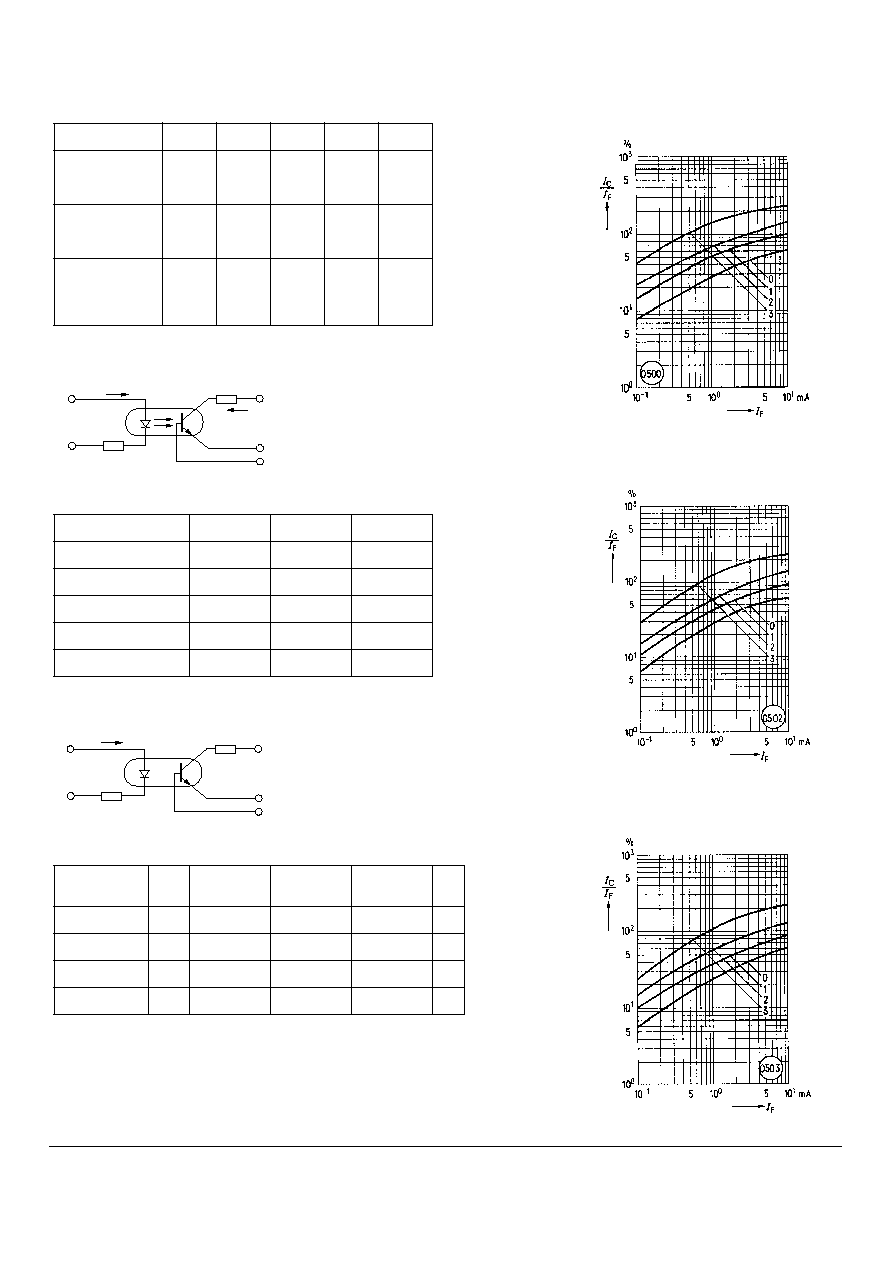
Current Transfer Ratio and Collector-Emitter Leakage Current
by dash number
(T
A
=25
°
C)
Figure 1. Linear Operation
(without saturation)
I
F
=10 mA, V
CC
=5 V, T
A
=25
°
C
Figure 2. Switching Operation
(with saturation)
-1
-2
-3
-4
Unit
I
C
/I
F
at V
CE
=5 V
(I
F
=10 mA)
40-80
63-
125
100-
200
160-
320
%
I
C
/I
F
at V
CE
=5 V
(I
F
=1 mA)
30
(>13)
45
(>22)
70
(>34)
90
(>56)
%
Collector-Emitter
Leakage Current
(V
CE
=10 V)
(I
CEO
)
2 (
50)
2 (
50)
5 (
100)
5 (
100)
nA
Load Resistance
R
L
75
Turn-On Time
t
ON
3.0
µ
s
Rise Time
t
R
2.0
µ
s
Turn-Off Time
t
OFF
2.3
µ
s
Fall Time
t
f
2.0
µ
s
Cut-off Frequency
f
CO
250
kHz
-1
(I
F
=20 mA)
-2 and -3
(I
F
=10 mA)
-4
(I
F
=5 mA)
Turn-On Time
t
ON
3.0
4.2
6.0
µ
s
Rise Time
t
R
2.0
3.0
4.6
µ
s
Turn-Off Time
t
OFF
18
23
25
µ
s
Fall Time
t
F
11
14
15
µ
s
R
L
=75
V
CC
=5 V
I
C
47
I
F
I
F
1 K
V
CC
=5 V
47
Figure 3. Current transfer ratio versus
diode current
(T
A
=25
°
C, V
CE
=5 V)
I
C
/I
F
=f (I
F
)
Figure 4. Current transfer ratio versus
diode current
(T
A
=0
°
C, V
CE
=5 V)
I
C
/I
F
=f (I
F
)
Figure 5. Current transfer ratio versus
diode current (T
A
=25
°
C, V
CE
=5 V)
I
C
/I
F
=f (I
F
)
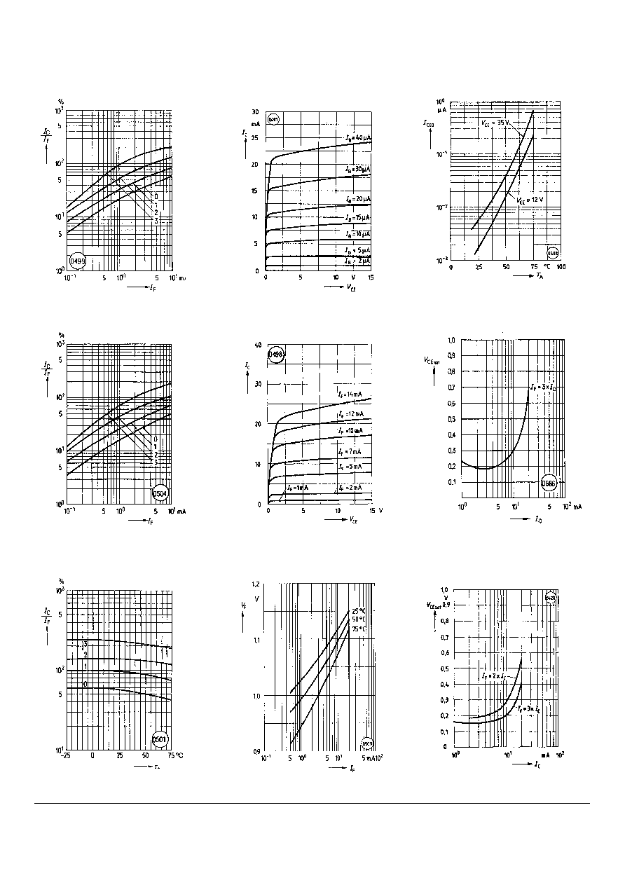
53
Figure 6. Current transfer ratio versus
diode current (T
A
=50
°
C)
V
CE
=5 V, I
C
/I
F
=f (I
F
)
Figure 7. Current transfer ratio versus
diode current (T
A
=75
°
C) V
CE
=5 V
Figure 8. Current transfer ratio versus
temperature (I
F
=10 mA, V
CE
=5 V)
I
C
/I
F
=f (T)
Figure 9. Transistor characteristics
(B=550) CNY17-3, -4 I
C
=f(V
CE
)
(T
A
=25
°
C, I
F
=0)
Figure 10. Output characteristics
CNY17-3, -4 (T
A
=25
°
C) I
C
=f(V
CE
)
Figure 11. Forward voltage V
F
=f (I
F
)
Figure 12. Collector emitter off-state
current I
CEO
=f (V, T) (T
A
=25
°
C, I
F
=0)
Figure 13. Saturation voltage versus
collector current and modulation
depth CNY17-1 V
CEsat
=f (I
C
) (T
A
=25
°
C)
Figure 14. Saturation voltage versus
collector current and modulation
depth CNY17-2 V
CEsat
=f (I
C
)
(T
A
=25
°
C )
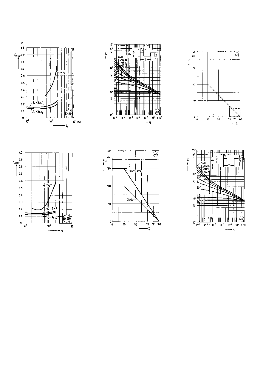
54
Figure 15. Saturation voltage versus
collector current and modulation
depth CNY17-3 V
CEsat
=f (I
C
) (T
A
=25
°
C)
Figure 16. Saturation voltage versus
collector current and modulation
depth CNY17-4 V
CEsat
=f (I
C
) (T
A
=25
°
C)
Figure 17. Permissible pulse load
D=parameter, T
A
=25
°
C, I
F
=f (t
p
)
Figure 18. Permissible power dissi-
pation transistor and diode
P
tot
=f (T
A
)
Figure 19. Permissible forward cur-
rent P
tot
=f (T
A
)
Figure 20. Transistor capacitance
C=f(V
O
) (T
A
=25
°
C, f=1 MHz)