PROFET® BTS 308
Semiconductor Group
1
12.96
Smart Highside Power Switch
Features
·
Overload protection
·
Current limitation
·
Short circuit protection
·
Thermal shutdown
·
Overvoltage protection (including load dump)
·
Fast demagnetization of inductive loads
·
Reverse battery protection
1)
·
Undervoltage and overvoltage shutdown with
auto-restart and hysteresis
·
Open drain diagnostic output
·
Open load detection in OFF-state
·
CMOS compatible input
·
Loss of ground and loss of
V
bb
protection
·
Electrostatic discharge (ESD) protection
Application
·
µ
C compatible power switch with diagnostic feedback for 12 V and 24 V DC grounded loads
·
Most suitable for inductive loads
·
Replaces electromechanical relays, fuses and discrete circuits
·
Fast switching
·
Not suitable for lamp loads
General Description
N channel vertical power FET with charge pump, ground referenced CMOS compatible input and diagnostic
feedback, monolithically integrated in Smart SIPMOS
®
technology. Fully protected by embedded protection
functions.
+ Vbb
IN
ST
Signal GND
ESD
PROFET
®
OUT
GND
Logic
Voltage
sensor
Voltage
source
Open load
detection
Short circuit
detection
Charge pump
Level shifter
Temperature
sensor
Rectifier
Limit for
unclamped
ind. loads
Gate
protection
Current
limit
2
4
1
3
5
Load GND
Load
V
Logic
Overvoltage
protection
1
)
With external current limit (e.g. resistor R
GND
=150
) in GND connection, resistor in series with ST
connection, reverse load current limited by connected load.
Product Summary
Overvoltage protection
V
bb(AZ)
60
V
Operating voltage
V
bb(on)
4.7 ... 34 V
On-state resistance
R
ON
300 m
Load current (ISO)
I
L(ISO)
1.3
A
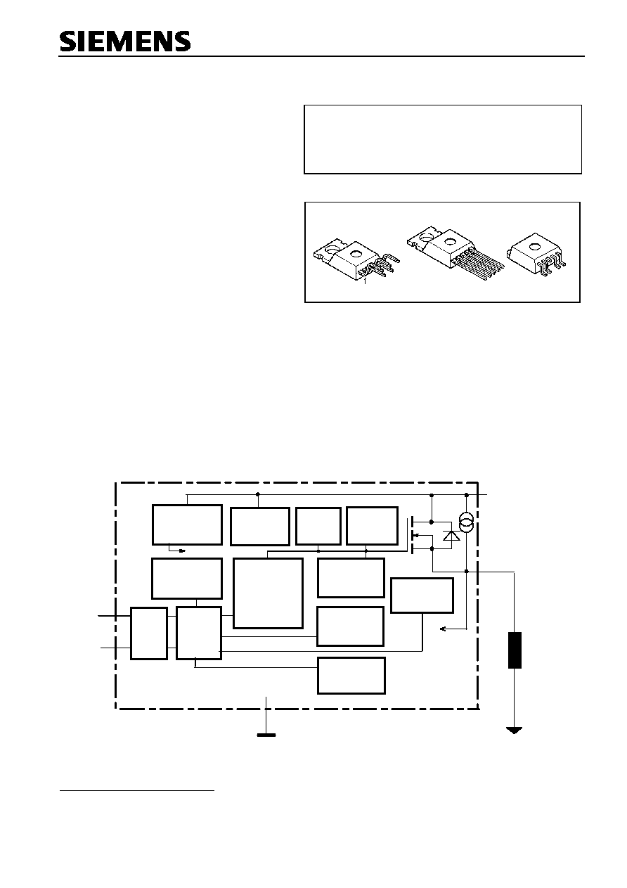
TO-220AB/5
5
Standard
1
5
Straight leads
1
5
SMD
BTS 308
Semiconductor Group
2
Pin
Symbol
Function
1
GND
-
Logic ground
2
IN
I
Input, activates the power switch in case of logical high signal
3
Vbb
+
Positive power supply voltage,
the tab is shorted to this pin
4
ST
S
Diagnostic feedback, low on failure
5
OUT
(Load, L)
O
Output to the load
Maximum Ratings at T
j
= 25 °C unless otherwise specified
Parameter
Symbol
Values
Unit
Supply voltage (overvoltage protection see page 3)
V
bb
60
V
Load current (Short circuit current, see page 4)
I
L
self-limited
A
Operating temperature range
Storage temperature range
T
j
T
stg
-40 ...+150
-55 ...+150
°C
Power dissipation (DC), T
C
25 °C
P
tot
50
W
Electrostatic discharge capability (ESD)
IN, ST:
(Human Body Model)
all other pins:
V
ESD
1
tbd (>1)
kV
Input voltage (DC)
V
IN
-10 ... +16
V
Current through input pin (DC)
Current through status pin (DC)
see internal circuit diagrams page 6
I
IN
I
ST
±
5.0
±
5.0
mA
Thermal resistance
chip - case:
junction - ambient (free air):
R
thJC
R
thJA
2.5
75
K/W

BTS 308
Semiconductor Group
3
Electrical Characteristics
Parameter and Conditions
Symbol
Values
Unit
at
T
j
= 25 °C,
V
bb
= 24 V unless otherwise specified
min
typ
max
Load Switching Capabilities and Characteristics
On-state resistance (pin 3 to 5)
I
L
= 0.8 A,
V
bb
= 12V
T
j
=25 °C:
T
j
=150 °C:
R
ON
--
270
540
300
600
m
Nominal load current, ISO Norm (pin 3 to 5)
V
ON
= 0.5 V,
T
C
= 85 °C
I
L(ISO)
1.18
1.3
--
A
Output current (pin
5
) while GND disconnected or
GND pulled up,
V
bb
=30 V,
V
IN
= 0, see diagram
page 7
I
L(GNDhigh)
--
--
1
mA
Turn-on time to 90%
V
OUT
:
Turn-off time to 10%
V
OUT
:
R
L
= 47
,
V
bb
= 12V,
T
j
=-40...+150°C
t
on
t
off
--
--
--
--
50
55
µ
s
Slew rate on, 10 to 30%
V
OUT
,
R
L
= 47
,
V
bb
= 12V,
T
j
=-40...+150°C
d
V /dt
on
1
--
10
V/
µ
s
Slew rate off, 10 to 30%
V
OUT
,
R
L
= 47
,
V
bb
= 12V,
T
j
=-40...+150°C
-d
V/dt
off
2
--
15
V/
µ
s
Operating Parameters
Operating voltage
2
)
T
j
=-40...+150°C:
V
bb(on)
4.7
--
34
V
Operating voltage slew rate
dV
bb
/
dt
-1
+1
V/
µ
s
Undervoltage shutdown
T
j
=25°C:
T
j
=-40...+150°C:
V
bb(under)
2.9
2.7
--
--
4.5
4.7
V
Undervoltage restart
T
j
=-40...+150°C:
V
bb(u rst)
--
--
4.9
V
Undervoltage restart of charge pump
see diagram page 11
T
j
=-40...+150°C:
V
bb(ucp)
--
4.9
7.5
V
Undervoltage hysteresis
V
bb(under)
=
V
bb(u rst)
-
V
bb(under)
V
bb(under)
--
0.2
--
V
Overvoltage shutdown
T
j
=-40...+150°C:
V
bb(over)
34
--
46
V
Overvoltage restart
T
j
=-40...+150°C:
V
bb(o rst)
34
--
--
V
Overvoltage hysteresis
T
j
=-40...+150°C:
V
bb(over)
--
0.5
--
V
Overvoltage protection
3
)
T
j
=-40...+150°C:
I
bb
=10 mA
V
bb(AZ)
59
70
--
V
Standby current (pin 3)
,
V
IN
=0
T
j
=-40...+150°C:
I
bb(off)
--
40
50
µ
A
Operating current (Pin 1)
4)
,
V
IN
=5 V
I
GND
--
2
4
mA
2)
At supply voltage increase up to
V
bb
= 4.9 V typ without charge pump,
V
OUT
V
bb
- 2 V
3)
Meassured without load
.
See also
V
ON(CL)
in table of protection functions and circuit diagram page 7.
4
)
Add
I
ST
, if
I
ST
> 0, add
I
IN
, if
V
IN
>5.5 V
BTS 308
Parameter and Conditions
Symbol
Values
Unit
at
T
j
= 25 °C,
V
bb
= 24 V unless otherwise specified
min
typ
max
Semiconductor Group
4
Protection Functions
Initial peak short circuit current limit (pin 3 to 5)
5
)
,
(
max 100
µ
s if
V
ON
>
V
ON(SC)
)
I
L(SCp)
V
bb
= 12V
T
j
=-40°C:
T
j
=25°C:
T
j
=+150°C:
2.0
2.8
2.0
--
5
--
10
6.2
5
A
Short circuit shutdown delay after input pos. slope
V
ON
>
V
ON(SC)
,
T
j
=-40..+150°C:
min value valid only, if input "low" time exceeds 60
µ
s
t
d(SC)
15
--
100
µ
s
Output clamp (inductive load switch off)
at
V
OUT
=
V
bb
-
V
ON(CL)
I
L
= 1 A,
T
j
=-40..+150°C:
V
ON(CL)
59
67
75
V
Short circuit shutdown detection voltage
(pin 3 to 5)
V
ON(SC)
--
3.5
--
V
Thermal overload trip temperature
T
jt
150
--
--
°C
Thermal hysteresis
T
jt
--
10
--
K
Reverse battery (pin 3 to 1)
6
)
-
V
bb
--
--
32
V
Diagnostic Characteristics
Open load detection current
T
j
=-40...+150°C:
(included in standby current
I
bb(off)
)
I
L(off)
0
--
30
µ
A
Open load detection voltage
T
j
=-40..150°C:
V
OUT(OL)
2
3
4
V
5
)
Short circuit current limit for max. duration of t
d(SC) max
=100
µ
s, prior to shutdown
6
)
Requires 150
resistor in GND connection. Reverse load current (through intrinsic drain-source diode) is
normally limited by the connected load. Input and Status currents have to be limited (see max. ratings page
2 and circuit page 7).

BTS 308
Parameter and Conditions
Symbol
Values
Unit
at
T
j
= 25 °C,
V
bb
= 24 V unless otherwise specified
min
typ
max
Semiconductor Group
5
Input and Status Feedback
7
)
Input resistance
see circuit page 6
R
I
--
4
--
k
Input turn-on threshold voltage
T
j
=-40..+150°C:
V
IN(T+)
1.5
--
2.4
V
Input turn-off threshold voltage
T
j
=-40..+150°C:
V
IN(T-)
0.8
--
--
V
Input threshold hysteresis,
T
j
=-40..+150°C
V
IN(T)
0.2
--
--
V
Off state input current (pin 2),
V
IN
= 0.4 V,
T
j
=-40..+150°C
I
IN(off)
8
--
30
µ
A
On state input current (pin 2),
V
IN
= 3.5 V,
T
j
=-40..+150°C
I
IN(on)
10
22
50
µ
A
Delay time for status with open load
after Input neg. slope (see diagram page 11)
t
d(ST OL3)
50
--
400
µ
s
Status invalid after positive input slope
(short circuit)
Tj=-40 ... +150°C:
t
d(ST SC)
15
50
100
µ
s
Status output (open drain)
Zener limit voltage
T
j
=-40...+150°C,
I
ST
= +50 uA:
ST low voltage
T
j
=-40...+150°C,
I
ST
= +1.6 mA:
V
ST(high)
V
ST(low)
5.4
--
6
--
--
0.4
V
7)
If a ground resistor R
GND
is used, add the voltage drop across this resistor.