Semiconductor Group
1
04.97
TEMPFET
®
BTS 112A
3
2
1
Features
q
N channel
q
Enhancement mode
q
Temperature sensor with thyristor characteristic
q
The drain pin is electricalIy shorted to the tab
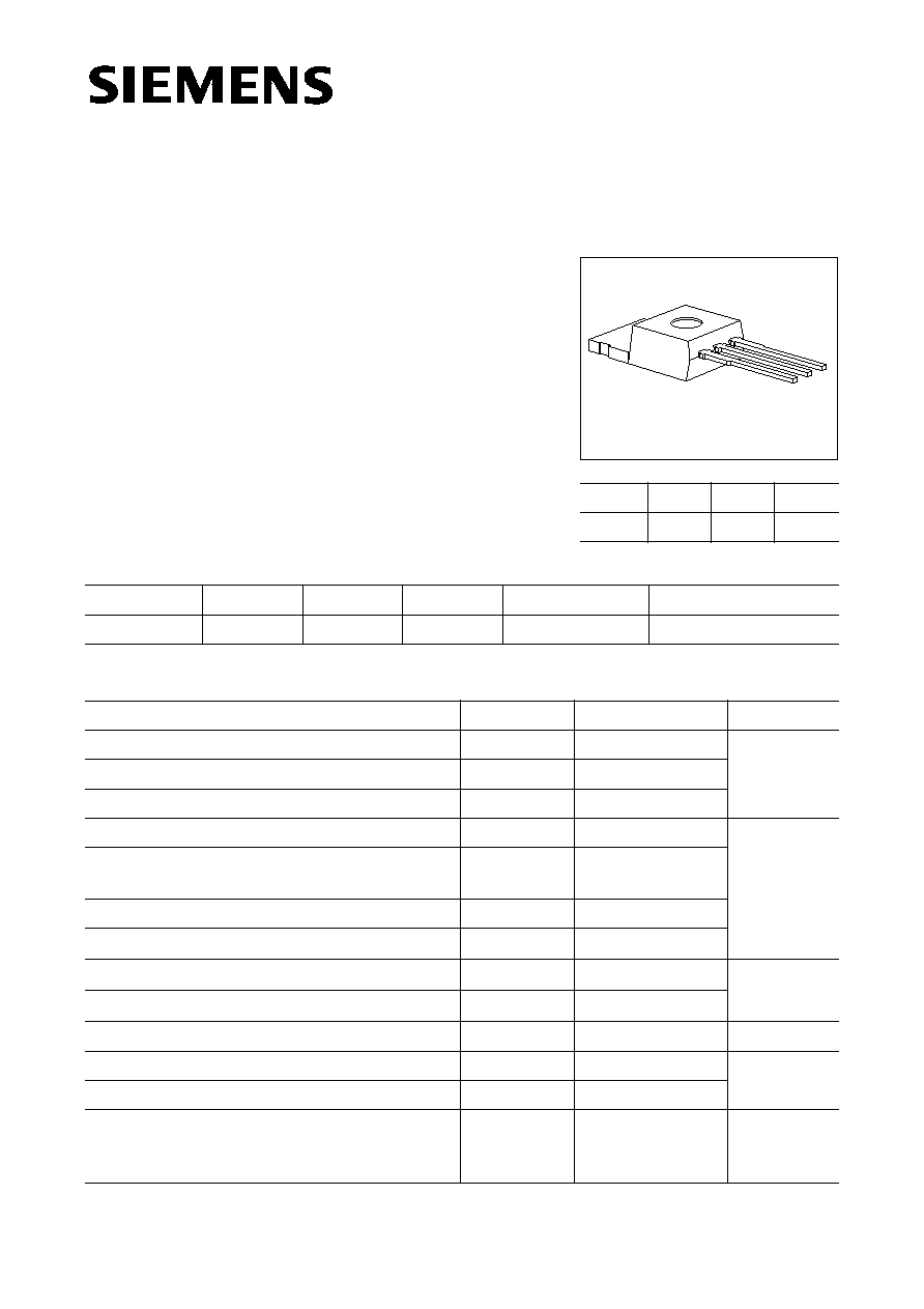
Pin
1
2
3
G
D
S
Type
V
DS
I
D
R
DS(on)
Package
Ordering Code
BTS 112A
60 V
12 A
0.15
TO-220AB
C67078-S5014-A3
Maximum Ratings
Parameter
Symbol
Values
Unit
Drain-source voltage
V
DS
60
V
Drain-gate voltage,
R
GS
= 20 k
V
DGR
60
Gate-source voltage
V
GS
±
20
Continuous drain current,
T
C
= 33
°
C
I
D
12
A
ISO drain current
T
C
= 85
°
C,
V
GS
= 10 V,
V
DS
= 0.5 V
I
D-ISO
2.5
Pulsed drain current,
T
C
= 25
°
C
I
D puls
48
Short circuit current,
T
j
= 55 ... + 150
°
C
I
SC
27
Short circuit dissipation,
T
j
= 55 ... + 150
°
C
P
SCmax
400
W
Power dissipation
P
tot
40
Operating and storage temperature range
T
j
,
T
stg
55 ... + 150
°
C
DIN humidity category, DIN 40 040
E
IEC climatic category, DIN IEC 68-1
55/150/56
Thermal resistance
Chip-case
Chip-ambient
R
th JC
R
th JA
3.1
75
K/W
Semiconductor Group
2
Electrical Characteristics
at
T
j
= 25 °C, unless otherwise specified.
Parameter
Symbol
Values
Unit
min.
typ.
max.
Static Characteristics
Drain-source breakdown voltage
V
GS
= 0
, I
D
= 0.25 mA
V
(BR)DSS
60
V
Gate threshold voltage
V
GS
=
V
DS
, I
D
= 1.0 mA
V
GS(th)
2.5
3.0
3.5
Zero gate voltage drain current
V
GS
= 60 V,
V
DS
= 0
T
j
= 25
°
C
T
j
= 150
°
C
I
DSS
0.1
10
1.0
100
µ
A
Gate-source leakage current
V
GS
=
±
20 V,
V
DS
= 0
T
j
= 25
°
C
T
j
= 150
°
C
I
GSS
10
2
100
4
nA
µ
A
Drain-source on-state resistance
V
GS
= 10 V
, I
D
= 7.5 A
R
DS(on)
0.12
0.15
Dynamic Characteristics
Forward transconductance
V
DS
2
×
I
D
×
R
DS(on)max
,
I
D
= 7.5 A
g
fs
3.0
5.7
S
Input capacitance
V
GS
= 0
, V
DS
= 25 V,
f
= 1 MHz
C
iss
360
480
pF
Output capacitance
V
GS
= 0
, V
DS
= 25 V,
f
= 1 MHz
C
oss
160
250
Reverse transfer capacitance
V
GS
= 0
, V
DS
= 25 V,
f
= 1 MHz
C
rss
50
90
Turn-on time
t
on
, (
t
on
=
t
d(on)
+
t
r
)
V
CC
= 30 V,
V
GS
= 10 V,
I
D
= 3 A,
R
GS
= 50
t
d(on)
15
25
ns
t
r
30
45
Turn-off time
t
off
, (
t
off
=
t
d(off)
+
t
f
)
V
CC
= 30 V,
V
GS
= 10 V,
I
D
= 3 A,
R
GS
= 50
t
d(off)
40
55
t
f
55
75
BTS 112A
Semiconductor Group
3
Electrical Characteristics (cont'd)
at
T
j
= 25
°
C, unless otherwise specified.
Parameter
Symbol
Values
Unit
min.
typ.
max.
Reverse Diode
Continuous source current
I
S
12
A
Pulsed source current
I
SM
48
Diode forward on-voltage
I
F
= 24 A,
V
GS
= 0
V
SD
1.5
1.8
V
Reverse recovery time
I
F
=
I
S
, d
i
F
/d
t
= 100 A/
µ
s,
V
R
= 30 V
t
rr
60
ns
Reverse recovery charge
I
F
=
I
S
, d
i
F
/d
t
= 100 A/
µ
s,
V
R
= 30 V
Q
rr
0.1
µ
C
Temperature Sensor
Forward voltage
I
TS(on)
= 10 mA,
T
j
= 55 ... + 150
°
C
Sensor override,
t
p
100
µ
s
T
j
= 55 ... + 160
°
C
V
TS(on)
1.4
1.5
10
V
Forward current
T
j
= 55 ... + 150
°
C
Sensor override,
t
p
100
µ
s
T
j
= 55 ... + 160
°
C
I
TS(on)
10
600
mA
Holding current,
V
TS(off)
= 5.0 V,
T
j
= 25
°
C
T
j
= 150
°
C
I
H
0.05
0.05
0.1
0.2
0.5
0.3
Switching temperature
V
TS
= 5.0 V
T
TS(on)
150
°
C
Turn-off time
V
TS
= 5.0 V,
I
TS(on)
= 2 mA
t
off
0.5
2.5
µ
s
BTS 112A
Semiconductor Group
4
Examples for short-circuit protection
at
T
j
= 55 ... + 150
°
C, unless otherwise specified.
Parameter
Symbol
Examples
Unit
1
2
Drain-source voltage
V
DS
15
30
V
Gate-source voltage
V
GS
6.8
5.0
Short-circuit current
I
SC
27
11
A
Short-circuit dissipation
P
SC
400
330
W
Response time
T
j
= 25
°
C, before short circuit
t
SC(off)
20
20
ms
BTS 112A
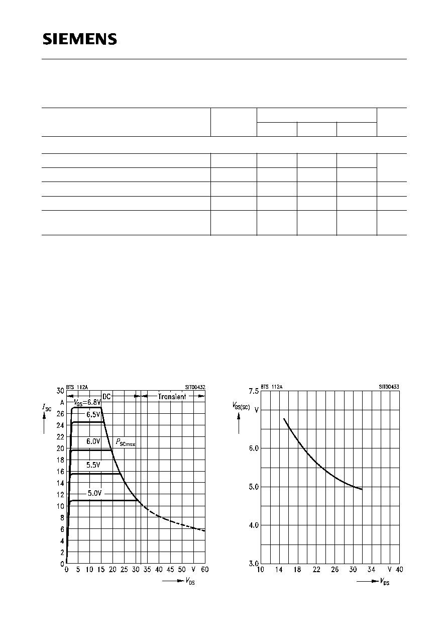
Short-circuit protection
I
SC
=
f
(
V
DS
)
Parameter
: V
GS
Diagram to determine
I
SC
for
T
j
= 55 ... +150
°
C
Max. gate voltage
V
GS(SC)
=
f
(
V
DS
)
Parameter:
T
j
= 55 ... + 150
°
C
Semiconductor Group
5
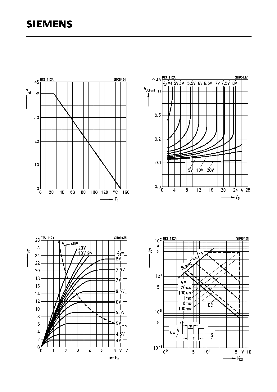
Max. power dissipation
P
tot
=
f
(
T
C
)
Typical output characteristics
I
D
=
f
(
V
DS
)
Parameter
: t
p
= 80
µ
s
Typ. drain-source on-state resistance
R
DS(on)
=
f
(
I
D
)
Parameter
: V
GS
Safe operating area
I
D
=
f
(
V
DS
)
Parameter:
D
= 0.01,
T
C
= 25
°
C
BTS 112A
Semiconductor Group
6
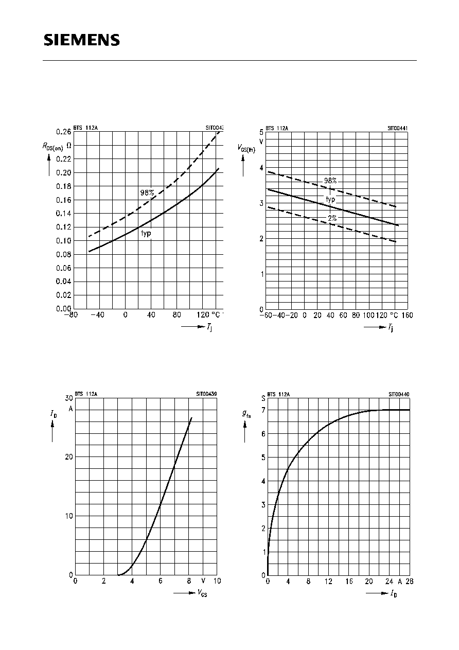
Drain-source on-state resistance
R
DS(on)
=
f
(
T
j
)
Parameter:
I
D
= 5 A,
V
GS
= 10 V
Typ. transfer characteristic
I
D
=
f
(
V
GS
)
Parameter
: t
p
= 80
µ
s,
V
DS
= 25 V
Gate threshold voltage
V
GS(th)
=
f
(
T
j
)
Parameter
: V
DS
=
V
GS
,
I
D
= 1 mA
Typ. transconductance
g
fs
=
f
(
I
D
)
Parameter:
t
p
= 80
µ
s,
V
DS
= 25 V
BTS 112A
Semiconductor Group
7
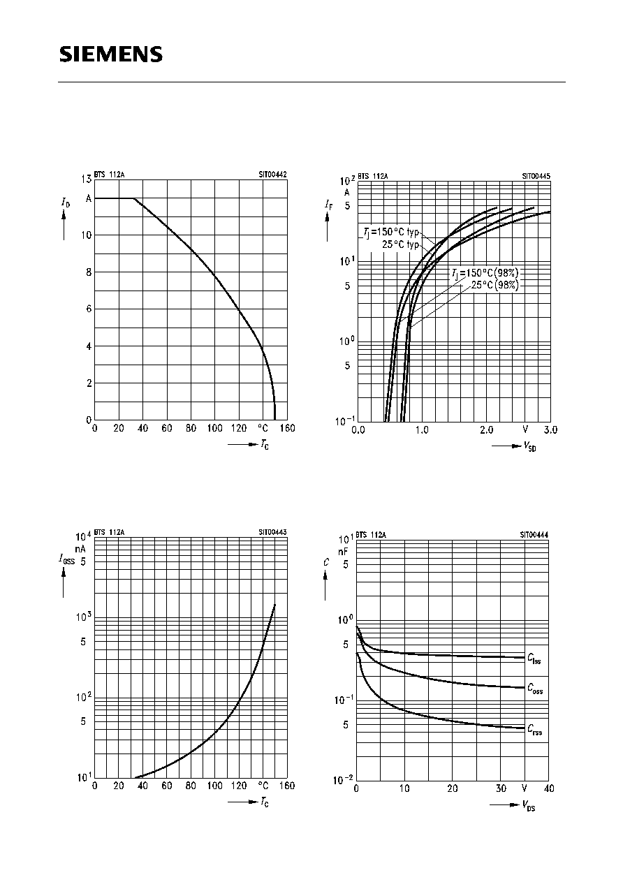
Continuous drain current
I
D
=
f
(
T
C
)
Parameter:
V
GS
10 V
Typ. gate-source leakage current
I
GSS
=
f
(
T
C
)
Parameter:
V
GS
= 20 V,
V
DS
= 0
Forward characteristics of reverse diode
I
F
=
f
(
V
SD
)
Parameter
: T
j
,
t
p
= 80
µ
s
Typ. capacitances
C
=
f
(
V
DS
)
Parameter:
V
GS
= 0,
f
= 1 MHz
BTS 112A
Semiconductor Group
8
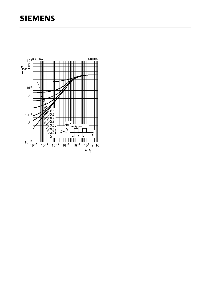
Transient thermal impedance
Z
thJC
=
f
(
t
p
)
Parameter
: D
=
t
p
/
T
BTS 112A
Semiconductor Group
9
BTS 112A
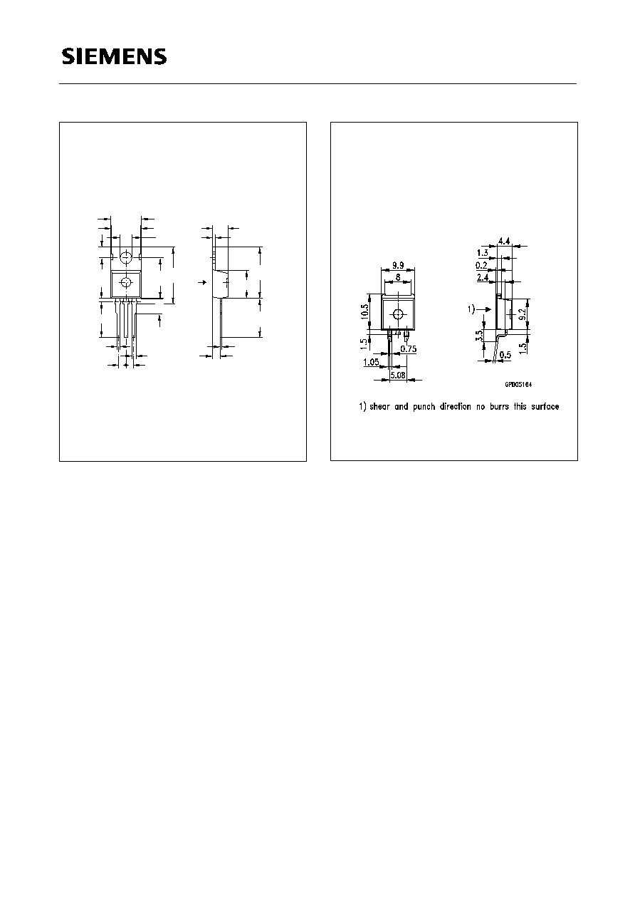
Package Outlines
TO 220 AB
Ordering Code
Standard
C67078-S5014-A3
TO 220 AB
Ordering Code
SMD Version E 3045
C67078-S5014-A4
Tape & reel E 3045 A
C67078-S5014-A5
3.7
9.5
9.9
4.6
0.75
1.05
2.54
2.54
17.5
2.8
12.8
0.5
2.4
13.5
9.2
15.6
1.3
4.4
GPT05155
1)
3) max. 14.5 by dip tinning press burr max. 0.05
2) dip tinning
1) punch direction, burr max. 0.04
3)
2)
1