Semiconductor Group
Jan-15-1998
Page 1
HITFET
®
®
BSP 78
Preliminary data
Smart Lowside Power Switch
Features
·
Logic Level Input
·
Input Protection (ESD)
·
Thermal shutdown with
auto restart
·
Overload protection
·
Short circuit protection
·
Overvoltage protection
·
Current limitation
·
Analog driving possible
Product Summary
Drain source voltage
V
40
V
DS
On-state resistance
R
DS(on)
50
m
Nominal load current
I
D(Nom)
3
A
Clamping energy
mJ
E
AS
500
Application
·
All kinds of resistive, inductive and capacitive loads in switching or linear
applications
·
µC compatible power switch for 12 V and 24 V DC applications
·
Replaces electromechanical relays and discrete circuits
General Description
N channel vertical power FET in Smart SIPMOS
®
technology. Fully protected by embedded
protection functions.
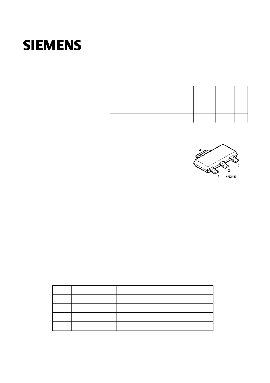
Pin
Symbol
Function
1
IN
Input
2
DRAIN
Output to the load
3
SOURCE
Ground
TAB
DRAIN
Output to the load
Semiconductor Group
Jan-15-1998
Page 2
Preliminary data
BSP 78
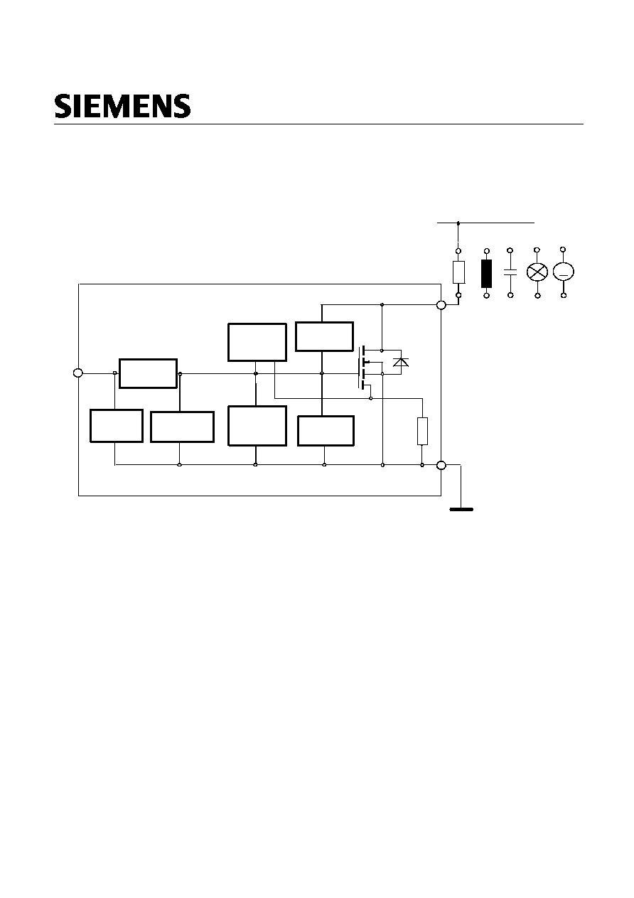
Block Diagram
p r o t e c t i o n
O v e r v o l t a g e
Drain
IN
E S D
H I T F E T
®
Source
C u r r e n t
O v e r -
p r o t e c t i o n
t e m p e r a t u r e
S h o r t c i r c u i t
p r o t e c t i o n
+
lim i t a t i o n
Vb b
S h o r t c i r c u i t
p r o t e c t i o n
L O A D
O v e r l o a d
p r o t e c t i o n
M
U n it
G a t e - D r i v i n g
Semiconductor Group
Jan-15-1998
Page 3
Preliminary data
BSP 78
Maximum Ratings at T
j
= 25°C, unless otherwise specified
Parameter
Value
Unit
Symbol
V
40
V
DS
Drain source voltage
Drain source voltage for
short circuit protection
40
V
DS(SC)
Continuous input voltage
V
IN
-0.2 ... +10
Peak input voltage (
I
IN
2 mA)
V
IN(peak)
-0.2 ...
V
DS
Operating temperature
T
j
°C
-40 ...+150
Storage temperature
T
stg
-55 ...+150
Power dissipation,
T
C
= 85 °C
P
tot
W
1.7
Unclamped single pulse inductive energy
F)
E
AS
500
mJ
Electrostatic discharge voltage
(Human Body Model)
according to MIL STD 883D, method 3015.7 and
EOS/ESD assn. standard S5.1 - 1993
2000
V
ESD
kV
E
DIN humidity category, DIN 40 040
IEC climatic category; DIN IEC 68-1
40/150/56
Thermal resistance
K/W
R
thJA
junction - ambient:
@ min. footprint
@ 6 cm
2
cooling area
F)
125
72
junction-soldering point:
R
thJS
17
K/W
1
not tested, specified by design
2
Device on 50mm+50mm*1.5mm epoxy PCB FR4 with 6 cm2 (one layer, 70µm thick) copper area for Drain
connection. PCB is vertical without blown air.

Semiconductor Group
Jan-15-1998
Page 4
Preliminary data
BSP 78
Electrical Characteristics
Parameter
Symbol
Unit
Values
at
T
j
= 25°C, unless otherwise specified
min.
max.
typ.
Characteristics
Drain source clamp voltage
T
j
= - 40 ...+ 150,
I
mess
= 10 mA
-
V
DS(AZ)
40
55
V
I
DSS
-
-
Off-state drain current
T
j
= -40 ... +150°C
V
IN
= 0 V,
V
DS
= 32 V
10
µA
Input treshold voltage
I
D
= 0.7 mA
1.7
1.3
V
2.2
V
IN(th)
I
IN(on)
On state input current
30
µA
10
-
R
DS(on)
On-state resistance
I
D
= 3 A,
V
IN
= 5 V,
T
j
= 25 °C
I
D
= 3 A,
V
IN
= 5 V,
T
j
= 150 °C
m
60
120
-
-
45
75
R
DS(on)
On-state resistance
I
D
= 3 A,
V
IN
= 10 V,
T
j
= 25 °C
I
D
= 3 A,
V
IN
= 10 V,
T
j
= 150 °C
50
100
35
65
-
-
I
D(Nom)
Nominal load current
V
DS
= 0.5 V,
T
S
= 85 °C,
T
j
< 150°C,
V
IN
= 10 V
-
-
A
3
A
I
D(lim)
Current limit (active if
V
DS
>2.5 V)
V
IN
= 10 V,
V
DS
= 12 V
16
24
32
Dynamic Characteristics
Turn-on time
V
IN
to 90%
I
D
:
R
L
= 5
,
V
IN
= 0 to 10 V,
V
bb
= 12 V
t
on
-
60
150
µs
Turn-off time
V
IN
to 10%
I
D
:
R
L
= 5
,
V
IN
= 10 to 0 V,
V
bb
= 12 V
t
off
-
60
150
Slew rate on 70 to 50%
V
bb
:
R
L
= 5
,
V
IN
= 0 to 10 V,
V
bb
= 12 V
-dV
DS
/dt
on
-
0.4
1
V/µs
Slew rate off 50 to 70%
V
bb
:
R
L
= 5
,
V
IN
= 10 to 0 V,
V
bb
= 12 V
dV
DS
/dt
off
-
0.7
1
Semiconductor Group
Jan-15-1998
Page 5
Preliminary data
BSP 78
Electrical Characteristics
Parameter
Symbol
Unit
Values
at
T
j
= 25°C, unless otherwise specified
typ.
min.
max.
Protection Functions
°C
150
T
jt
Thermal overload trip temperature
165
-
Thermal hysteresis
T
jt
-
10
K
-
300
Input current protection mode
-
-
I
IN(Prot)
µA
Unclamped single pulse inductive energy
F)
I
D
= 3 A,
T
j
= 25 °C,
V
bb
= 12 V
I
D
= 3 A,
T
j
= 150 °C,
V
bb
= 12 V
E
AS
500
300
-
-
-
-
mJ
Inverse Diode
Continuous source drain voltage
V
IN
= 0 V, -
I
D
= 5*3 A,
t
P
= 300 µs
-
1.1
-
V
V
SD
1
not tested, specified by design