
Mini PROFET® BSP 452
Semiconductor Group
1
08.96
MiniPROFET
·
High-side switch
·
Short-circuit protection
·
Input protection
·
Overtemperature protection with hysteresis
·
Overload protection
·
Overvoltage protection
·
Switching inductive load
·
Clamp of negative output voltage with inductive loads
·
Undervoltage shutdown
·
Maximum current internally limited
·
Electrostatic discharge (ESD) protection
·
Reverse battery protection
1)
Package: SOT 223
Type
Ordering code
BSP 452
Q67000-S271
Application
·
µ
C compatible power switch for 12 V DC grounded loads
·
All types of resistive, inductive and capacitive loads
·
Replaces electromechanical relays and discrete circuits
General Description
N channel vertical power FET with charge pump, ground referenced CMOS compatible input,monolithically
integrated in Smart SIPMOS
®
technology. Fully protected by embedded protection functions.
Blockdiagramm:
IN
3
R
in
+ Vbb
Signal GND
ESD
MINI-PROFET
OUT
GND
Logic
Voltage
sensor
Voltage
source
Charge pump
Level shifter
Temperature
sensor
Rectifier
Limit for
unclamped
ind. loads
Gate
protection
Current
limit
2
4
1
Load GND
Load
V
Logic
Overvoltage
protection
ESD-
Diode
1) With resistor RGND=150
in GND connection, resistor in series with IN connections reverse load current
limited by connected load.
1
2
3
4

Mini PROFET® BSP 452
Semiconductor Group
2
Pin
Symbol
Function
1
OUT
O
Output to the load
2
GND
-
Logic ground
3
IN
I
Input, activates the power switch in case of logical high signal
4
Vbb
+
Positive power supply voltage
Maximum Ratings
at
T
j
= 25 °C unless otherwise specified
Parameter
Symbol
Values
Unit
Supply voltage
V
bb
40
V
Load current
self-limited
I
L
I
L(SC)
A
Maximum input voltage
2)
V
IN
-5.0...
V
bb
V
Maximum input current
I
IN
±
5
mA
Inductive load switch-off energy dissipation,
single pulse
I
L
= 0.5A , T
A
= 150°C
(not tested, specified by design)
E
AS
0.5
J
Load dump protection
3
)
V
LoadDump
=
U
A
+
V
s
R
L
= 24
R
I
=2
,
t
d
=400ms, IN= low or high,
U
A
=12V
R
L
= 80
(not tested, specified by design)
V
Load dump
4
)
47
67
V
Electrostatic discharge capability (ESD)
5)
PIN 3
PIN 1,2,4
V
ESD
±
1
±
2
kV
Operating temperature range
Storage temperature range
T
j
T
stg
-40 ...+150
-55 ...+150
°C
Max. power dissipation (DC)
6)
T
A
= 25 °C
P
tot
1.8
W
Thermal resistance
chip - soldering point:
chip - ambient:
6)
R
thJS
R
thJA
7
70
K/W
2) At V
IN > Vbb, the input current is not allowed to exceed
±
5 mA.
3) Supply voltages higher than Vbb(AZ) require an external current limit for the GND pin, e.g. with a 150
resistor in the GND connection
A resistor for the protection of the input is integrated.
4) VLoad dump is setup without the DUT connected to the generator per ISO 7637-1 and DIN 40839
5) HBM according to MIL-STD 883D, Methode 3015.7
6) BSP 452 on epoxy pcb 40 mm x 40 mm x 1.5 mm with 6 cm2 copper area for V
bb connection

Mini PROFET® BSP 452
Semiconductor Group
3
Electrical Characteristics
Parameter and Conditions
Symbol
Values
Unit
at
T
j
= 25 °C,
V
bb = 13.5V unless otherwise specified
min
typ
max
Load Switching Capabilities and Characteristics
On-state resistance (pin 4 to 1)
I
L
= 0.5 A,
V
in
= high
T
j
= 25°C
T
j
= 150°C
R
ON
--
--
0.16
--
0.2
0.4
Nominal load current (pin 4 to 1)
7)
ISO Standard:
V
ON
=
V
bb
-
V
OUT
= 0.5 V
T
S
= 85 °C
I
L(ISO)
1.7
--
--
A
Turn-on time
to 90%
V
OUT
Turn-off time
to 10%
V
OUT
R
L
= 24
t
on
t
off
--
--
60
60
100
150
µ
s
Slew rate on
10 to 30%
V
OUT
,
R
L
= 24
d
V /dt
on
--
2
4
V/
µ
s
Slew rate off
70 to 40%
V
OUT
,
R
L
= 24
-d
V/dt
off
--
2
4
V/
µ
s
Input
Allowable input voltage range, (pin 3 to 2)
V
IN
-3.0
--
V
bb
V
Input turn-on threshold voltage
T
j
= -40...+150°C
V
IN(T+)
--
--
3.5
V
Input turn-off threshold voltage
T
j
= -40...+150°C
V
IN(T-)
1.5
--
--
V
Input threshold hysteresis
V
IN(T)
--
0.5
--
V
Off state input current (pin 3)
V
IN(off)
= 1.2 V
T
j
= -40...+150°C
I
IN(off)
10
--
60
µ
A
On state input current (pin 3)
V
IN(on)
= 3.0 V to
V
bb
T
j
= -40...+150°C
I
IN(on)
10
--
100
µ
A
Input resistance
R
IN
1.5
2.8
3.5
k
7
)
IL(ISO) characterizes the MOSFET part of the device and may be higher than the shortcircuit current IL(SC) of the whole device

Mini PROFET® BSP 452
Semiconductor Group
4
Parameter and Conditions
Symbol
Values
Unit
at
T
j
= 25 °C,
V
bb = 13.5V unless otherwise specified
min
typ
max
Operating Parameters
Operating voltage
8
)
T
j
=-40...+150°C
V
bb(on)
5.0
--
34
V
Undervoltage shutdown
T
j
=-40...+150°C
V
bb(under)
3.5
--
5
V
Undervoltage restart
T
j
=-40...+25°C
T
j
=+150°C
V
bb(u rst)
--
--
6.5
7.0
V
Undervoltage restart of charge pumpe
see diagram page 7
V
bb(ucp)
--
5.6
7
V
Undervoltage hysteresis
V
bb(under)
=
V
bb(u rst)
-
V
bb(under)
V
bb(under)
--
0.3
--
V
Overvoltage shutdown
T
j
=-40...+150°C
V
bb(over)
34
--
42
V
Overvoltage restart
T
j
=-40...+150°C
V
bb(o rst)
33
--
--
V
Overvoltage hysteresis
T
j
=-40...+150°C
V
bb(over)
--
0.7
--
V
Standby current (pin 4),
V
in
= low
T
j
=-40...+150°C
I
bb(off)
--
10
25
µ
A
Operating current (pin 2),
V
in
= 5 V
I
GND
--
1
1.6
mA
leakage current (pin 1)
V
in
= low
T
j
=-40...+25°C
T
j
=150°C
I
L(off)
--
2
5
7
µ
A
Protection Functions
Current limit (pin 4 to 1)
T
j
= 25°C
V
bb
= 20V
T
j
= -40...+150°C
I
L(SC)
0.7
0.7
1.5
--
2
2.4
A
Overvoltage protection
Ibb=4mA T
j
=-40...+150°C
V
bb(AZ)
41
--
--
V
Output clamp (ind. load switch off)
at
V
OUT
=
V
bb
-
V
ON(CL),
I
bb
= 4mA
V
ON(CL)
41
47
--
V
Thermal overload trip temperature
T
jt
150
--
--
°C
Thermal hysteresis
T
jt
--
10
--
K
Inductive load switch-off energy dissipation
9
)
T
j Start
= 150 °C, single pulse,
I
L
= 0.5 A,
V
bb
= 12 V
(not tested, specified by design)
E
AS
--
--
0.5
J
Reverse battery (pin 4 to 2)
10
)
(not tested, specified by design)
-
V
bb
--
--
30
V
8) At supply voltage increase up to Vbb= 5.6 V typ without charge pump, VOUT
Vbb - 2 V
9) While demagnetizing load inductance, dissipated energy in PROFET is EAS=
VON(CL) * iL(t) dt, approx.
EAS= 1/2 * L * I
2
L
* (
VON(CL)
VON(CL) - Vbb
)
10) Requires 150
resistor in GND connection. Reverse load current (through intrinsic drain-source diode) is normally limited by the
connected load.
Mini PROFET® BSP 452
Semiconductor Group
5
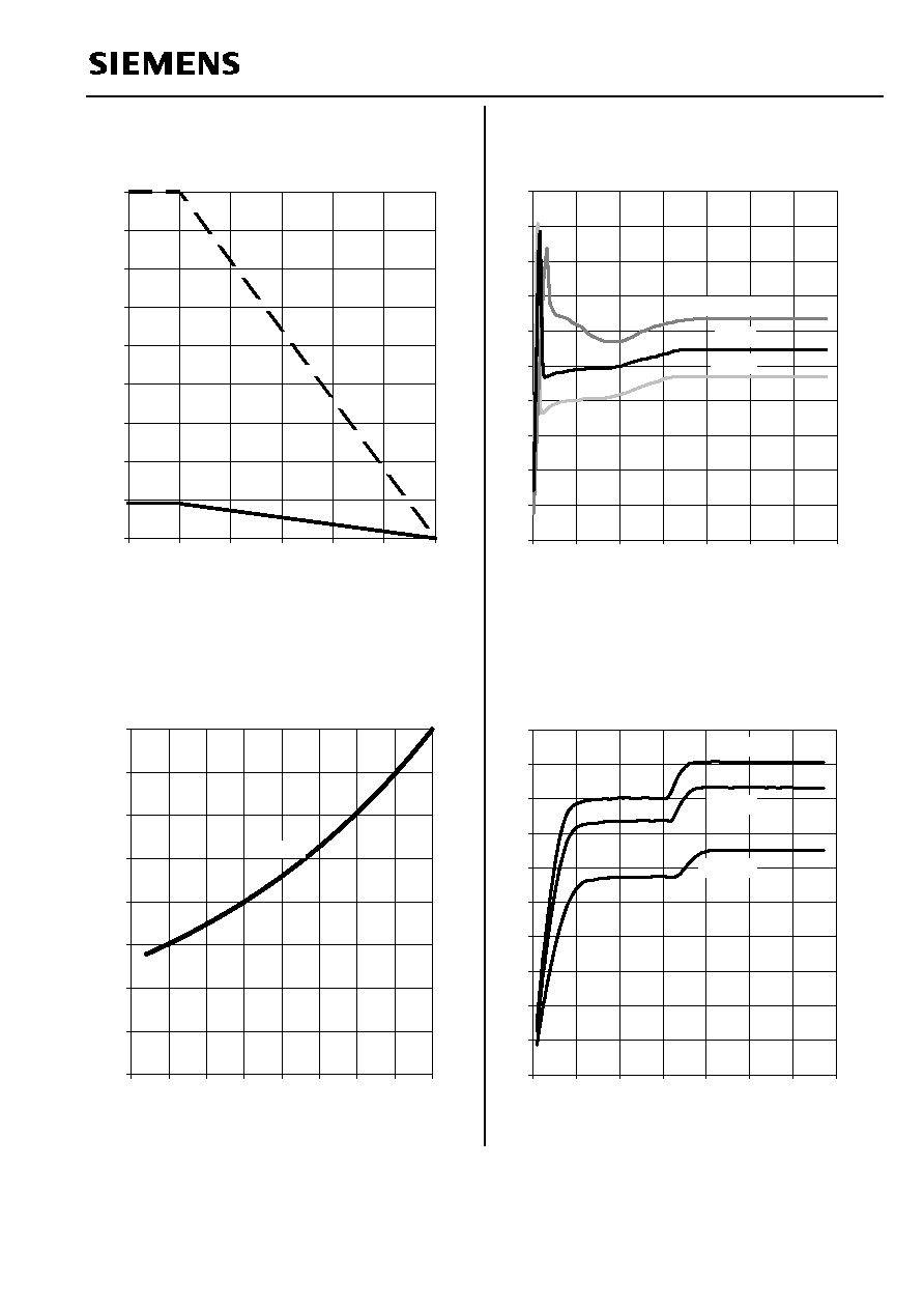
Max. allowable power dissipation
Ptot = f (TA,TSP)
Ptot [W]
0
2
4
6
8
10
12
14
16
18
0
25
50
75
100
125
150
T
A
T
SP
TA, TSP[°C]
On state resistance (Vbb-pin to OUT-pin)
RON = f (Tj); Vbb = 13.5 V; IL = 0.5 A
RON [
]
0
0.05
0.1
0.15
0.2
0.25
0.3
0.35
0.4
-50
-25
0
25
50
75
100
125
150
98%
Tj [°C]
Current limit characteristic
IL(SC) = f (Von); (Von see testcircuit)
IL(SC) [A]
0
0.2
0.4
0.6
0.8
1
1.2
1.4
1.6
1.8
2
0
2
4
6
8
10
12
14
25°C
150°C
-40°C
Von [V]
Typ. input current
IIN = f (VIN); Vbb = 13,5 V
IIN [µA]
0
5
10
15
20
25
30
35
40
45
50
0
2
4
6
8
10
12
14
-40°C
+ 150°C
+ 25°C
VIN [V]