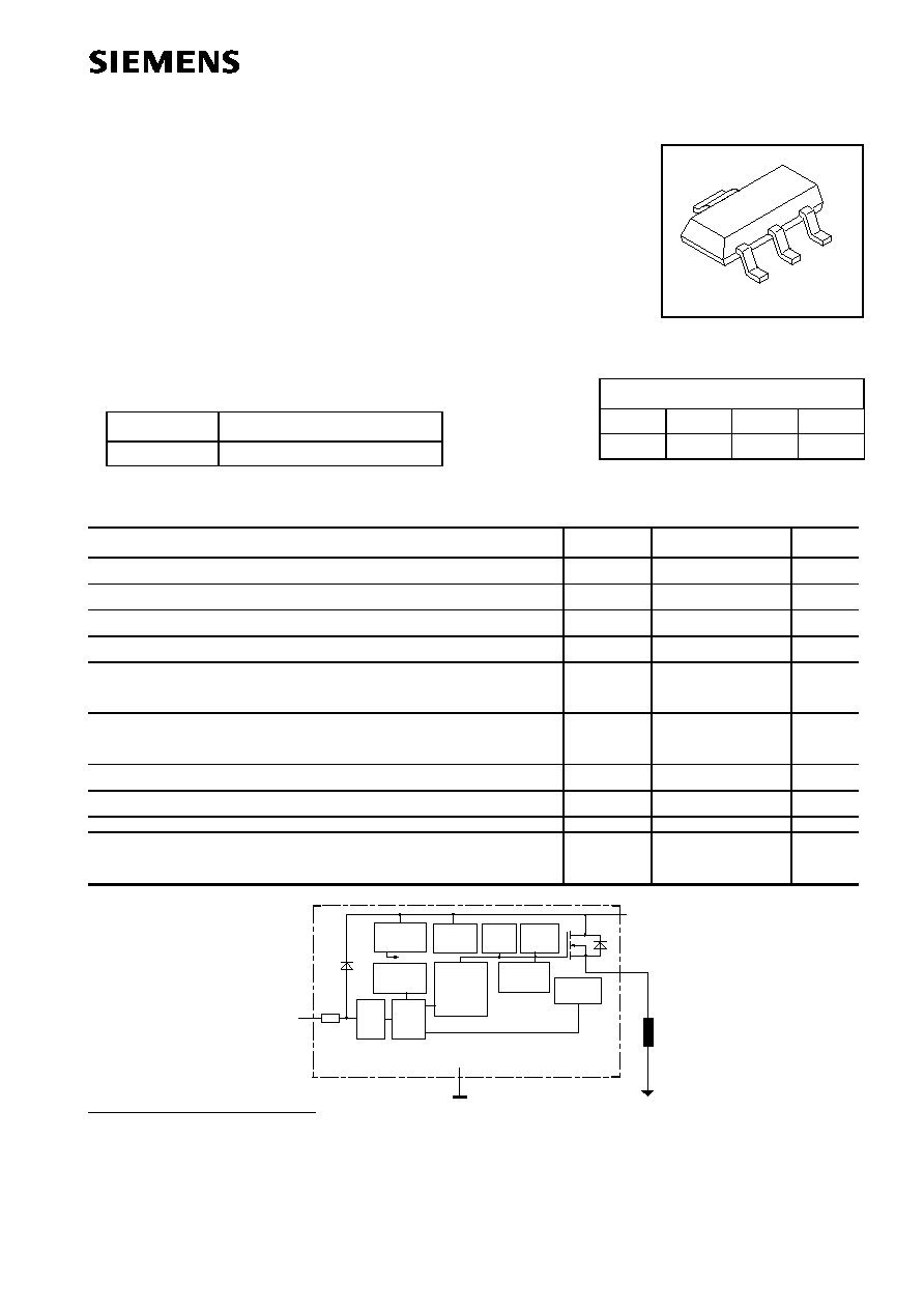
Mini PROFET® BSP 450
Semiconductor Group
1
06.96
MiniPROFET
·
High-side switch
·
Short-circuit protection
·
Input protection
·
Overtemperature protection with hysteresis
·
Overload protection
·
Overvoltage protection
·
Switching inductive load
·
Clamp of negative output voltage with inductive loads
·
Undervoltage shutdown
·
Maximum current internally limited
·
Electrostatic discharge (ESD) protection
·
Reverse battery protection
1)
Package: SOT 223
Type
Ordering code
BSP 450
Q67000-S266
Maximum Ratings
Parameter
Symbol
Values
Unit
Supply voltage range
V
bb
-0.3...48
V
Load current
self-limited
I
L
I
L(SC)
A
Maximum input voltage
2)
V
IN
-5.0...
V
bb
V
Maximum input current
I
IN
±
5
mA
Inductive load switch-off energy dissipation
single pulse
I
L
= 0.5A ,
T
A
= 85°C
E
AS
0.5
J
Operating temperature range
Storage temperature range
T
j
T
stg
-40 ...+125
-55 ...+150
°C
Max. power dissipation (DC)
3
)
T
A
= 25 °C
P
tot
1.4
W
Electrostatic discharge capability (ESD)
4)
V
ESD
±
1
kV
Thermal resistance
chip - soldering point:
chip - ambient
3)
R
thJS
R
thJA
7
70
K/W
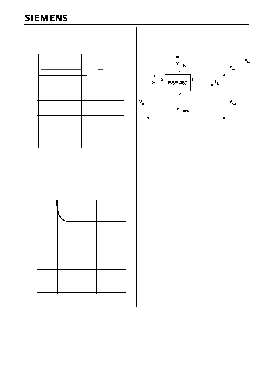
IN
3
R
in
+ Vbb
Signal GND
ESD
MINI-PROFET
OUT
GND
Logic
Voltage
sensor
Voltage
source
Charge pump
Level shifter
Temperature
sensor
Rectifier
Limit for
unclamped
ind. loads
Gate
protection
Current
limit
2
4
1
Load GND
Load
V
Logic
Overvoltage
protection
ESD-
Diode
1) With resistor R
GND
=150
in GND connection, resistor in series with IN connections reverse load current
limited by connected load.
2) At V
IN
> V
bb
, the input current is not allowed to exceed
±
5 mA.
3) BSP 450 on epoxy pcb 40 mm x 40 mm x 1.5 mm with 6 cm2 copper area for V
bb
connection
4) HBM according to MIL-STD 883D, Methode 3015.7
1
2
3
4
Pins
1
2
3
4
OUT
GND
IN
V
bb
BSP 450
Semiconductor Group
2
Electrical Characteristics
Parameter and Conditions
Symbol
Values
Unit
at
T
j
= 25 °C,
V
bb = 24V unless otherwise specified
min
typ
max
Load Switching Capabilities and Characteristics
On-state resistance (pin 4 to 1)
I
L
= 0.5 A,
V
in
= high
T
j
= 25°C
T
j
= 125°C
R
ON
--
--
0.16
--
0.2
0.38
Nominal load current (pin 4 to 1)
5)
ISO Standard:
V
ON
=
V
bb
-
V
OUT
= 0.5 V
T
S
= 85 °C
I
L(ISO)
1.7
--
--
A
Turn-on time
to 90%
V
OUT
Turn-off time
to 10%
V
OUT
R
L
= 47
t
on
t
off
--
--
60
90
100
150
µ
s
Slew rate on
10 to 30%
V
OUT
,
R
L
= 47
d
V /dt
on
--
2
4
V/
µ
s
Slew rate off
70 to 40%
V
OUT
,
R
L
= 47
-d
V/dt
off
--
2
4
V/
µ
s
Input
Allowable input voltage range, (pin 3 to 2)
V
IN
-3.0
--
V
bb
V
Input turn-on threshold voltage
Vbb = 18...30V
T
j
= -25...+125°C
V
IN(T+)
--
--
3.0
V
Input turn-off threshold voltage
Vbb = 18...30V
T
j
= -25...+125°C
V
IN(T-)
1.82
--
--
V
Input threshold hysteresis
V
IN(T)
--
0.1
--
V
Off state input current (pin 3)
V
IN(off)
= 1.82 V
T
j
= -25...+125°C
I
IN(off)
20
--
--
µ
A
On state input current (pin 3)
V
IN(on)
= 3.0 V to
V
bb
T
j
= -25...+125°C
I
IN(on)
--
--
110
µ
A
Input resistance
T
j
= -25...+125°C
R
IN
1.5
2.8
3.5
k
5) I
L(ISO)
characterizes the MOSFET part of the device and may be higher than the shortcircuit current I
L(SC)
of the whole device
BSP 450
Parameter and Conditions
Symbol
Values
Unit
at
T
j
= 25 °C,
V
bb = 24V unless otherwise specified
min
typ
max
Semiconductor Group
3
Operating Parameters
Operating voltage
T
j
=-25...+125°C
V
bb(on)
12
--
40
V
Undervoltage shutdown
T
j
=-25...+125°C
V
bb(under)
7
--
10.5
V
Undervoltage restart
T
j
=-25...+125°C:
V
bb(u rst)
--
--
11
V
Undervoltage hysteresis
V
bb(under)
--
0.4
--
V
Standby current (pin 4),
V
in
= low
T
j
=-25...+100°C
T
j
=125°C
6)
I
bb(off)
--
10
25
50
µ
A
Operating current (pin 2),
V
in
= high
T
j
=-25...+125°C
I
GND
--
1
1.6
mA
leakage current (pin 1)
V
in
= low
T
j
=-25...+125°C
I
L(off)
--
--
2
µ
A
Protection Functions
Current limit (pin 4 to 1)
T
j
= 25°C
T
j
= -25...+125°C
I
L(SC)
0.7
0.7
1.5
--
2
2.4
A
Overvoltage protection
I
bb
=4mA
T
j
=-25...+125°C
V
bb(AZ)
48
--
--
V
Output clamp (ind. load switch off)
at
V
OUT
=
V
bb
-
V
ON(CL),
I
bb
= 4mA
V
ON(CL)
--
72
--
V
Thermal overload trip temperature
T
jt
135
150
--
°C
Thermal hysteresis
T
jt
--
10
--
K
Inductive load switch-off energy dissipation
7)
T
j Start
= 85 °C, single pulse,
I
L
= 0.5 A,
V
bb
= 12 V
E
AS
--
--
0.5
J
Reverse Battery
Reverse battery voltage
8
)
-V
bb
30
V
Continious reverse drain current
T
A
= 25°C
-I
S
--
--
1
A
Drain-Source diode voltage
I
F
= 1 A,
V
in
= low
V
OUT
>
V
bb
-V
ON
--
--
1.2
V
6) increase of standby current at T
j
= 125°C caused by temperature sense current
7) while demagnetizing load inductance, dissipated energy is E
AS
=
(VON(CL) * iL(t) dt,
approx.
E
AS
= 1/2 * L * I
2
L
* (
VON(CL)
VON(CL)-Vbb
)
8) Requires 150
resistor in GND connection. Reverse load current (through intrinsic drain-source diode)
is normally limited by the connected load.
BSP 450
Semiconductor Group
4
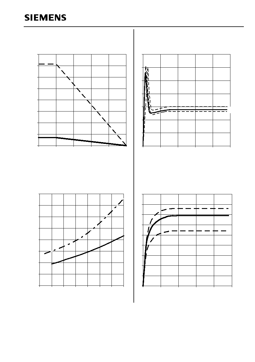
Max allowable power dissipation
Ptot = f (TA,TSP)
Ptot [W]
0
2
4
6
8
1 0
1 2
1 4
1 6
0
2 5
5 0
7 5
1 0 0
1 2 5
T
T
S P
A
TA, TSP[°C]
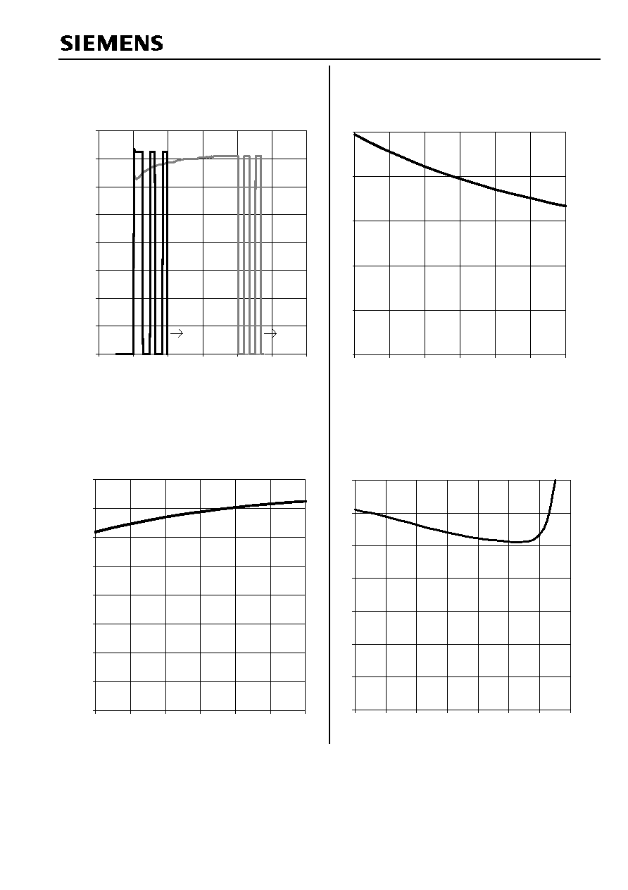
On state resistance (Vbb-pin to OUT pin)
RON = f (Tj);Vbb = 24 V;IL = 0.5 A
RON [
]
0
0.05
0.1
0.15
0.2
0.25
0.3
0.35
0.4
-50
-25
0
25
50
75
100
125
98%
T
j
[°C]
Current limit characteristic
IL(SC) = f (Von) (Von see testcircuit)
IL(SC) [A]
0
0.5
1
1.5
2
2.5
3
3.5
0
5
10
15
20
25
25°C
125°C
-25°C
V
on
[V]
Typ. input current
IIN = f(VIN); Vbb = 24 V
IIN [
µ
A]
0
10
20
30
40
50
60
70
80
90
0
5
10
15
20
25
125°C
25°C
-25°C
V
IN
[V]
BSP 450
Semiconductor Group
5
Typ. overload current
IL(lim) = f (t), Vbb=24V, no heatsink, Param.:Tjstart
IL(lim) [A]
0
0.2
0.4
0.6
0.8
1
1.2
1.4
1.6
-20
0
20
40
60
80
100
125°C
-25°C
t [ms]
Short circuit current
IL(SC) = f (Tj);Vbb = 30 V;
IL(SC) [
]
0
0.2
0.4
0.6
0.8
1
1.2
1.4
1.6
-25
0
25
50
75
100
125
Tj [°C]
Typ. operating current
IGND = f (Tj), Vbb=30V, VIN=high
GND [mA]
0
0.2
0.4
0.6
0.8
1
-25
0
25
50
75
100
125
Tj [°C]
Typ. standby current
Ibb(off) = f(Tj); Vbb = 30 V, VIN = low
Ibb(off) [
µ
A]
0
1
2
3
4
5
6
7
-25
0
25
50
75
100
125
150
Tj [°C]
BSP 450
Semiconductor Group
6
Typ. input turn on voltage threshold
VIN(T+) = f (Tj)
VIN(T+) [V]
0
0.5
1
1.5
2
2.5
3
-25
0
25
50
75
100
125
30V
18V
Tj [°C]
Typ. on-state resistance (Vbb-Pin to OUT-Pin)
RON = f (Vbb,IL); IL = 0.5A, Tj = 25 °C;
RON [m
]
0
20
40
60
80
100
120
140
160
0
5
10
15
20
25
30
35
40
45
Vbb [V]
Test circuit
BSP 450
Semiconductor Group
7
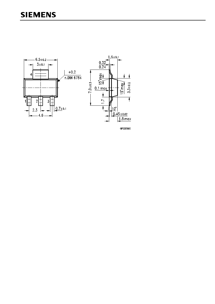
Package:
all dimensions in mm.
SOT 223/4: