
BPY 62
Semiconductor Group
238
NPN-Silizium-Fototransistor
Silicon NPN Phototransistor
BPY 62
1)
Eine Lieferung in dieser Gruppe kann wegen Ausbeuteschwankungen nicht immer sichergestellt werden.
Wir behalten uns in diesem Fall die Lieferung einer Ersatzgruppe vor.
1)
Supplies out of this group cannot always be guaranteed due to unforseeable spread of yield. In this case we
will reserve us the right of delivering a substitute group.
Typ
Type
Bestellnummer
Ordering Code
BPY 62
Q60215-Y62
BPY 62-2
Q60215-Y1111
BPY 62-3
Q60215-Y1112
BPY 62-4
Q60215-Y1113
BPY 62-5
1)
Q62702-P1113
Maße in mm, wenn nicht anders angegeben/Dimensions in mm, unless otherwise specified
fmof6019
Wesentliche Merkmale
q
Speziell geeignet für Anwendungen im
Bereich von 420 nm bis 1130 nm
q
Hohe Linearität
q
Hermetisch dichte Metallbauform (TO-18)
mit Basisanschlu
, geeignet bis 125
°
C
q
Gruppiert lieferbar
Anwendungen
q
Lichtschranken für Gleich- und
Wechsellichtbetrieb
q
Industrieelektronik
q
"Messen/Steuern/Regeln"
Features
q
Especially suitable for applications from
420 nm to 1130 nm
q
High linearity
q
Hermetically sealed metal package (TO-18)
with base connection suitable up to 125
°
C
q
Available in groups
Applications
q
Photointerrupters
q
Industrial electronics
q
For control and drive circuits
10.95

Semiconductor Group
239
BPY 62
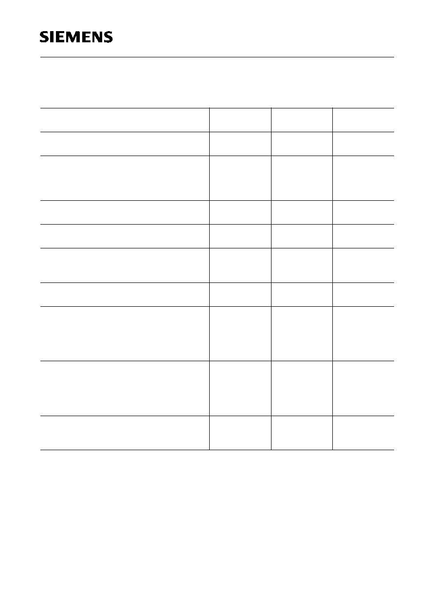
Grenzwerte
Maximum Ratings
Bezeichnung
Description
Symbol
Symbol
Wert
Value
Einheit
Unit
Betriebs- und Lagertemperatur
Operating and storage temperature range
T
op
;
T
stg
55 ... + 125
°
C
Löttemperatur bei Tauchlötung
Lötstelle
2 mm vom Gehäuse,
Lötzeit
t
5 s
Dip soldering temperature
2 mm distance
from case bottom, soldering time
t
5 s
T
S
260
°
C
Löttemperatur bei Kolbenlötung
Lötstelle
2 mm vom Gehäuse,
Lötzeit
t
3 s
Iron soldering temperature
2 mm distance
from case bottom, soldering time
t
3 s
T
S
300
°
C
Kollektor-Emitterspannung
Collector-emitter voltage
V
CE
50
V
Kollektorstrom
Collector current
I
C
100
mA
Kollektorspitzenstrom,
<
10
µ
s
Collector surge current
I
CS
200
mA
Emitter-Basisspannung
Emitter-base voltage
V
EB
7
V
Verlustleistung,
T
A
= 25
°
C
Total power dissipation
P
tot
200
mW
Wärmewiderstand
Thermal resistance
R
thJA
500
K/W
BPY 62
Semiconductor Group
240
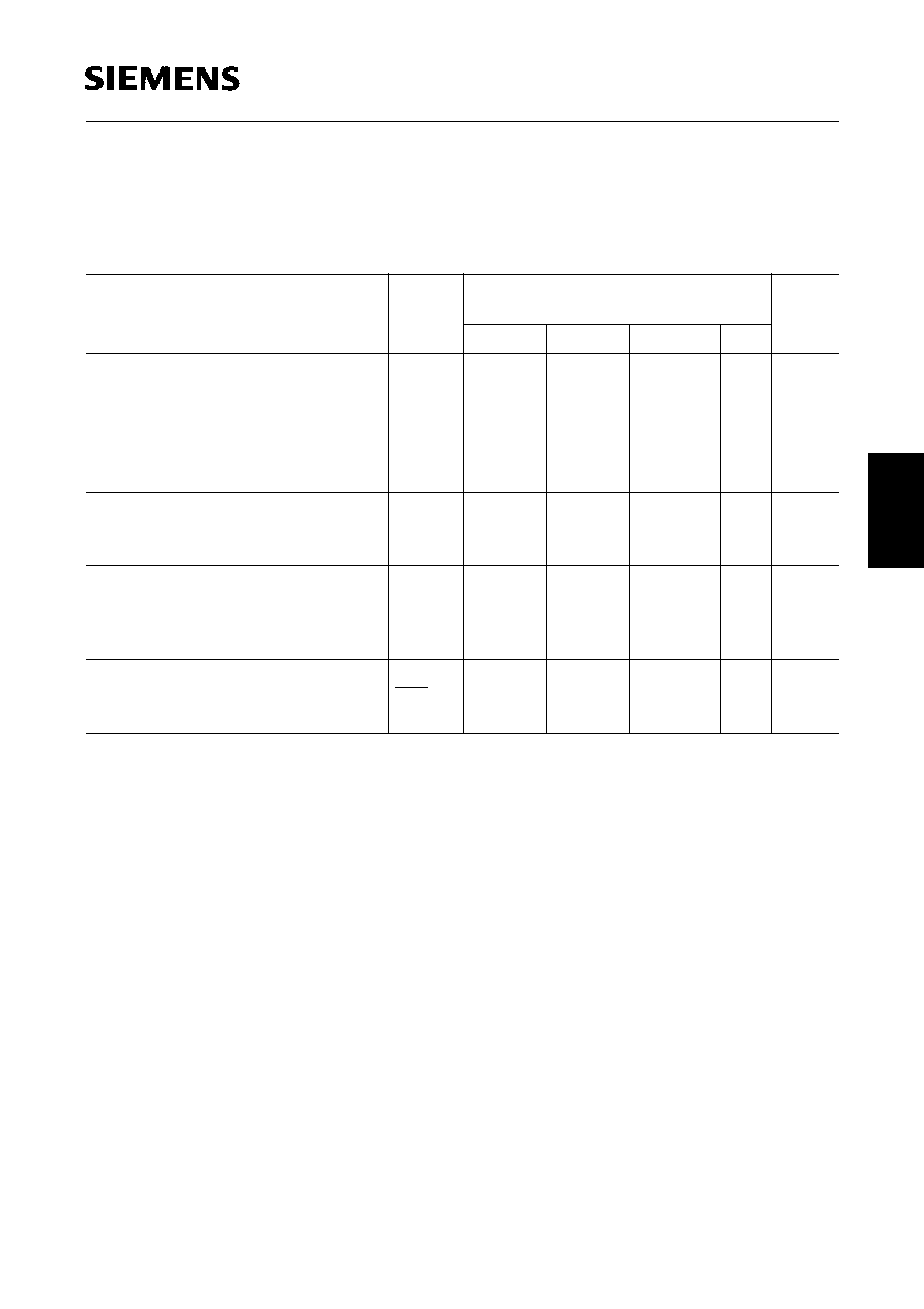
Kennwerte (
T
A
= 25
°
C,
= 950 nm)
Characteristics
Bezeichnung
Description
Symbol
Symbol
Wert
Value
Einheit
Unit
Wellenlänge der max. Fotoempfindlichkeit
Wavelength of max. sensitivity
S max
850
nm
Spektraler Bereich der Fotoempfindlichkeit
S
= 10 % von
S
max
Spectral range of sensitivity
S
= 10 % of
S
max
420 ... 1130
nm
Bestrahlungsempfindliche Fläche
Radiant sensitive area
A
0.12
mm
2
Abmessung der Chipfläche
Dimensions of chip area
L
×
B
L
×
W
0.5
×
0.5
mm
×
mm
Abstand Chipoberfläche zu Gehäuseober-
fläche
Distance chip front to case surface
H
2.4 ... 3.0
mm
Halbwinkel
Half angle
±
8
Grad
deg.
Fotostrom der Kollektor-Basis-Fotodiode
Photocurrent of collector-base photodiode
E
e
= 0.5 mW/cm
2
,
V
CB
= 5 V
E
v
= 1000 Ix, Normlicht/standard light A,
V
CB
= 5 V
I
PCB
I
PCB
4.5
17
µ
A
µ
A
Kapazität
Capacitance
V
CE
= 0 V,
f
= 1 MHz,
E
= 0
V
CB
= 0 V,
f
= 1 MHz,
E
= 0
V
EB
= 0 V,
f
= 1 MHz,
E
= 0
C
CE
C
CB
C
EB
8
11
19
pF
pF
pF
Dunkelstrom
Dark current
V
CE
= 35 V,
E
= 0
I
CEO
5 (
100)
nA
Semiconductor Group
241
BPY 62
Die Fototransistoren werden nach ihrer Fotoempfindlichkeit gruppiert und mit arabischen
Ziffern gekennzeichnet.
The phototransistors are grouped according to their spectral sensitivity and distinguished
by arabian figures.
1)
I
PCEmin
ist der minimale Fotostrom der jeweiligen Gruppe
1)
I
PCEmin
is the min. photocurrent of the specified group
Bezeichnung
Description
Symbol
Symbol
Wert
Value
Einheit
Unit
-2
-3
-4
-5
Fotostrom,
=
950 nm
Photocurrent
E
e
= 0.5 mW/cm
2
,
V
CE
= 5 V
E
v
= 1000 Ix, Normlicht/standard light
A,
V
CE
= 5 V
I
PCE
I
PCE
0.5 ... 1.0
3.0
0.8 ... 1.6
4.6
1.25 ... 2.5
7.2
2.0
11.4
mA
mA
Anstiegszeit/Abfallzeit
Rise and fall time
I
C
= 1 mA,
V
CC
= 5 V,
R
L
= 1 k
t
r
,
t
f
5
7
9
12
µ
s
Kollektor-Emitter-Sättigungsspannung
Collector-emitter saturation voltage
I
C
=
I
PCEmin
1)
×
0.3,
E
e
= 0.5 mW/cm
2
V
CEsat
150
150
160
180
mV
Stromverstärkung
Current gain
E
e
= 0.5 mW/cm
2
,
V
CE
= 5 V
I
PCE
I
PCB
170
270
420
670

BPY 62
Semiconductor Group
242
Relative spectral sensitivity
S
rel
=
f
(
)
Output characteristics
I
C
=
f
(
V
CE
),
I
B
= Parameter
Photocurrent
I
PCE
/
I
PCE25
o
=
f
(
T
A
),
V
CE
= 5 V
Photocurrent
I
PCE
=
f
(
E
e
),
V
CE
= 5 V
Output characteristics
I
C
=
f
(
V
CE
),
I
B
= Parameter
Dark current
I
CEO
/
I
CEO25
o
=
f
(
T
A
),
V
CE
= 25 V,
E
= 0
Total power dissipation
P
tot
=
f
(
T
A
)
Dark current
I
CEO
=
f
(
V
CE
),
E
= 0
Collector-emitter capacitance
C
CE
=
f
(
V
CE
),
f
= 1 MHz,
E
= 0