Semiconductor Group
1
BCX 41
BSS 64
NPN Silicon AF and Switching Transistor
BCX 41
BSS 64
Maximum Ratings
Type
Ordering Code
(tape and reel)
Marking
Package
1)
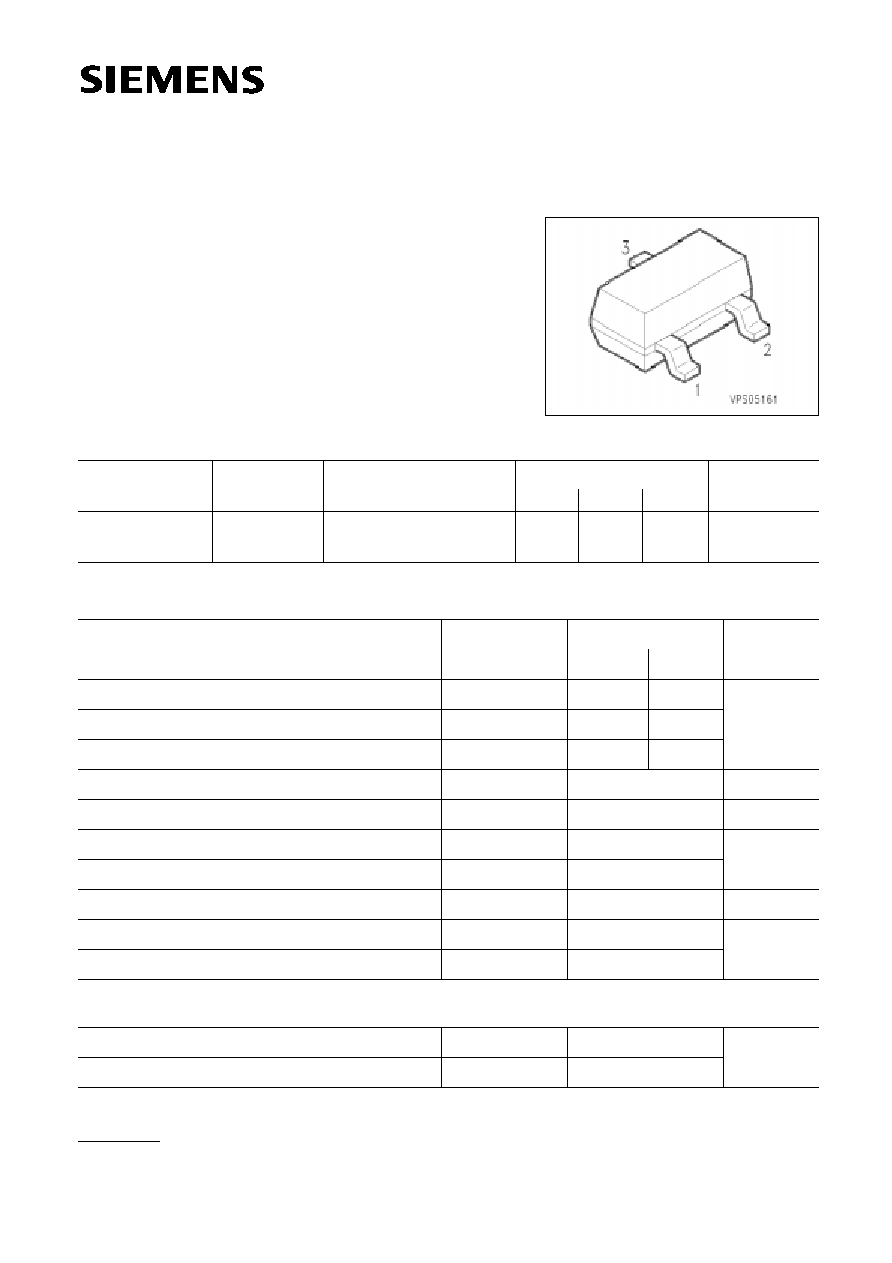
Pin Configuration
BCX 41
BSS 64
Q62702-C1659
Q62702-S535
EKs
AMs
SOT-23
B
E
C
1
2
3
Parameter
Symbol
Values
Unit
Collector-emitter voltage
V
CE0
80
V
Collector-base voltage
V
CB0
120
Emitter-base voltage
V
EB0
5
Collector current
I
C
800
mA
Peak collector current
I
CM
1
A
Base current
I
B
100
mA
Peak base current
I
BM
200
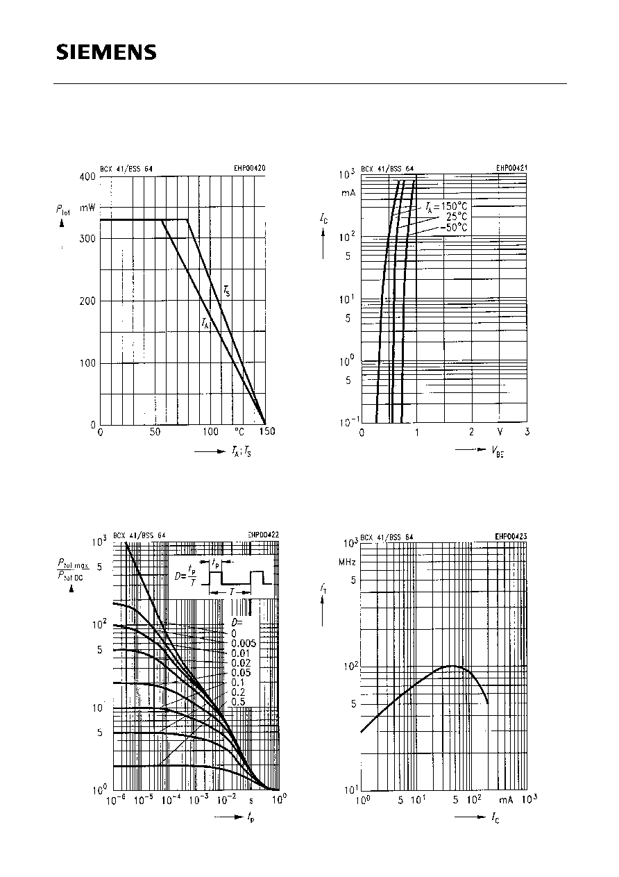
Total power dissipation,
T
S
= 79 �C
P
tot
330
mW
Junction temperature
T
j
150
�C
Storage temperature range
T
stg
� 65 ... + 150
Thermal Resistance
Junction - ambient
2)
R
th JA
285
K/W
125
125
5
BSS 64
BCX 41
Junction - soldering point
R
th JS
215
1)
For detailed information see chapter Package Outlines.
2)
Package mounted on epoxy pcb 40 mm
�
40 mm
�
1.5 mm/6 cm
2
Cu.
q
High breakdown voltage
q
Low collector-emitter saturation voltage
q
Complementary types: BCX 42, BSS 63 (PNP)
5.91
Semiconductor Group
2
BCX 41
BSS 64
Electrical Characteristics at
T
A
= 25 �C, unless otherwise specified.
Unit
Values
Parameter
Symbol
min.
typ.
max.
DC characteristics
V
Collector-emitter breakdown voltage
I
C
= 10 mA
BSS 64
BCX 41
V
(BR)CE0
80
125
�
�
�
�
MHz
Transition frequency
I
C
= 20 mA
, V
CE
= 5 V,
f
= 20 MHz
f
T
�
100
�
pF
Output capacitance
V
CB
= 10 V,
f
= 1 MHz
C
obo
�
12
�
AC characteristics
Collector-base breakdown voltage
1)
I
C
= 100
�
A
BSS 64
BCX 41
V
(BR)CB0
120
125
�
�
�
�
�
A
Collector cutoff current
V
CE
= 100 V
T
A
= 85 �C
BCX 41
T
A
= 125 �C
BCX 41
I
CE0
�
�
�
�
10
75
Emitter-base breakdown voltage
I
E
= 10
�
A
V
(BR)EB0
5
�
�
nA
nA
�
A
�
A
Collector cutoff current
V
CB
= 80 V
BSS 64
V
CB
= 100 V
BCX 41
V
CB
= 80 V,
T
A
= 150 �C
BSS 64
V
CB
= 100 V,
T
A
= 150 �C
BCX 41
I
CB0
�
�
�
�
�
�
�
�
100
100
20
20
�
DC current gain
1)
I
C
= 100
�
A,
V
CE
= 1 V
BCX 41
I
C
= 1 mA,
V
CE
= 1 V
BSS 64
I
C
= 4 mA,
V
CE
= 1 V
BSS 64
I
C
= 10 mA,
V
CE
= 1 V
BSS 64
I
C
= 20 mA,
V
CE
= 1 V
BSS 64
I
C
= 100 mA,
V
CE
= 1 V
BCX 41
I
C
= 200 mA,
V
CE
= 1 V
BCX 41
h
FE
25
�
20
�
�
63
40
�
60
80
80
55
�
�
�
�
�
�
�
�
�
V
Collector-emitter saturation voltage
1)
I
C
= 300 mA,
I
B
= 30 mA
BCX 41
I
C
= 4 mA,
I
B
= 0.4 mA
BSS 64
I
C
= 50 mA,
I
B
= 15 mA
BSS 64
V
CEsat
�
�
�
�
�
�
0.9
0.7
3.0
Base-emitter saturation voltage
1)
I
C
= 300 mA,
I
B
= 30 mA
BCX 41
V
BEsat
�
�
1.4
nA
Emitter cutoff current
V
EB
= 4 V
I
EB0
�
�
100
1)
Pulse test:
t
300
�
s,
D
= 2 %