s
Applications
Parameter
Symbol
Rating
Unit
Input
I
F
mA
Reverse voltage
V
R
V
Power dissipation
P
mW
Output
V
CC
V
V
V
iso
Operating temperature
T
opr
°C
Storage temperature
T
stg
°C
T
sol
260
°C
s
Features
s
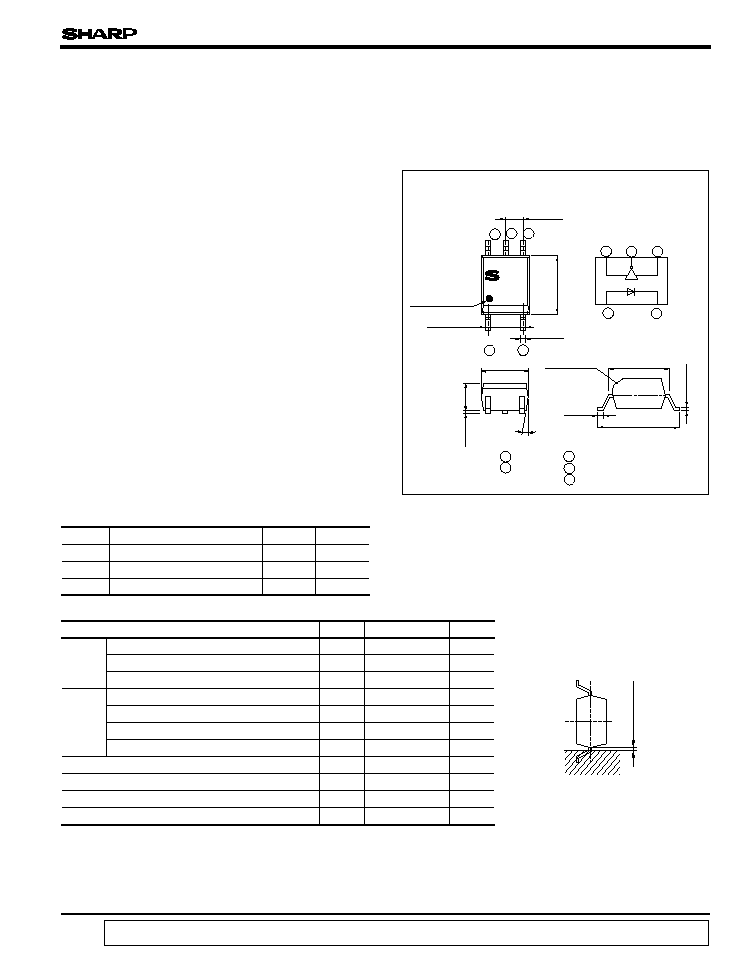
Outline Dimensions
( Unit : mm )
1. Hybrid substrate which requires high den-
2. Personal computers, office computers and
sity mounting
peripheral equipment
High level output voltege
Low level output current
V
OH
I
OL
P
O
50
- 40 to + 125
mA
mW
( Ta = 25°C)
s
Absolute Maximum Ratings
PC410
1. Mini-flat package
2. Ultra-high speed response
3. Isolation voltage between input and output
( V
iso
rms
)
Output collector power dissipation
20
40
7
7
85
0 to + 70
4. Audio equipment
3. Electronic musical instruments
PC410
( t
PLH
, t
PHL
: TYP. 50ns at R
L
= 350
)
voltage CM
H
: TYP. 500V/
µ
s
s
Package Specifications
*1 Ta = 0 to + 70°C
*4 For 10 seconds.
*1
Forward current
*2
Supply voltage
*4
*3
Isolation voltege
1
6 Vcc
3
6
5
4
1
3
Anode mark
Internal connection
diagram
6
5
4
PC410
Soldering area
0.2mm or more
*3 AC for 1 minute, 40 to 60% RH. Apply the specified voltage between the whole of the
*2 For 1 minute MAX.
electrode pins on the input side and the whole of the electrode pins on the output side.
data books, etc. Contact SHARP in order to obtain the latest version of the device specification sheets before using any SHARP's device.
"
"
In the absence of confirmation by device specification sheets, SHARP takes no responsibility for any defects that occur in equipment using any of SHARP's devices, shown in catalogs,
1 Anode
3 Cathode
6
°
(Input Side)
Diameter of reel
Tape width
12 mm
12 mm
-
-
Compact, Surface Mount
Ultra-high Speed Response
OPIC Photocoupler
An OPIC consists of a light-detecting element and signal-
processing circuit integrated onto a single chip.
* " OPIC " ( Optical IC ) is a trademark of the SHARP Corporation.
4 GND
5 Vo
5
Soldering temperature
: 2 500 V
4. Instantaneous common mode rejection
5. Recognized by UL(No.64380)
Model No.
Package specifications
PC410
PC410T
Taping package
( Net: 750pcs.)
PC410Z
Sleeve package
( Net: 100pcs.)
2 500
Taping package
( Net:3 000pcs. )
370 mm
180 mm
C0.4
4.4
±
0.2
1.27
±
0.25
2.54
±
0.25
0.4
±
0.1
2.6
±
0.2
0.1
±
0.1
3.6
±
0.3
5.3
±
0.3
0.2
±
0.05
0.5
+
0.4
-
0.2
7.0
+
0.2
-
0.7
V
rms
s
Electro-optical Characteristics
Parameter
Symbol
Conditions
Input
Forward voltage
V
F
Reverse current
I
R
Ta = 25°C, V
R
= 5V
Terminal capacitance
C
t
Output
Transfer
charac-
teristics
High level supply current
I
CCH
" H
L " threshold input current
I
FHL
Isolation resistance
R
ISO
Floating capacitance
t
PHL
t
PLH
t
f
t
r
CM
H
CM
L
V
CC
= 5.5V, I
F
= 0
V
CC
= 5V, V
O
= 0.8V, R
L
= 350
Ta = 25°C, DC500V, 40 to 60% RH
Ta = 25°C, V = 0, f = 1MHz
Ta = 25°C
V
CC
= 5V, I
F
R
L
= 350
, C
L
= 15pF
Fig. 1
I
F
= 0
V
O
(MIN. ) = 2V
I
F
= 5mA
V
O
(MAX.) = 0.8V
Low level output voltage
High level output current
Low level supply current
V
OL
I
CCL
I
OH
Ta = 25°C, I
F
= 10mA
Ta = 25°C, V = 0, f = 1MH
Z
I
OL
= 13mA, V
CC
= 5.5V, I
F
= 5mA
V
CC
= V
O
= 5.5V, I
F
V
CC
= 5.5V, I
F
= 10mA
Note ) All typical values : at Ta = 25°C, V
CC
= 5V
Each characteristics shall be measured under opaque condition.
Ta = 25°C
V
CC
= 5V
R
L
= 350
Fig. 2
V
CM
= 10V(Peak )
s
Recommended Operation Conditions
PC410
( Ta = 0 to + 70°C unless otherwise specified )
Connect a by-pass ceramic capacitor ( 0.01 to 0.1
µ
F ) between V
CC
and GND at the
position within 1cm from lead pin.
Parameter Symbol
MIN.
MAX.
Unit
Low level input current
I
FL
0 250
µ
A
High level input current
I
FH
7 15
mA
Supply voltage
V
CC
4.5 5.5 V
Fanout
( TTL load ) N
-
8
-
Operating temperature
T
opr
0 70
°C
MIN.
TYP.
MAX.
Unit
-
1.6
1.9
V
-
-
10
µ
A
-
60
150
0.6
V
-
2
250
µ
A
-
13
18
mA
-
7
15
mA
-
2.5
5
mA
5 x 10
10
10
11
-
-
0.6
pF
-
-
50
120
ns
-
50
120
-
30
60
-
30
60
100
500
-
V/
µ
s
- 100
- 500
-
" H
L " propagation
delay time
" L
H " propagation
delay time
Fall time
Response
Rise time
CMR
time
C
f
0.4
-
Instantaneous common
mode rejection
voltage " High level
output "
Instantaneous common
mode rejection
voltage " Low level
output "
= 7.5mA
pF
= 250 m A

PC410
10
20
100
40
30
0
0
70 75
100
50
60
70
80
90
85
Collector power dissipation P
C
(
mW
)
Ambient temperature T
a
(°C)
50°C
25°C
70°C
1.0
0.01
0.1
1
10
100
1.2
1.4
1.6
1.8
2.0
2.2
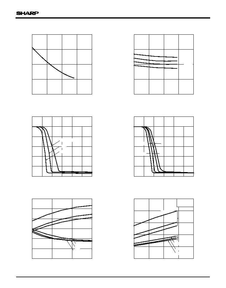
Fig. 4 Forward Current vs.
Forward Voltage
Fig. 3 Collector Power Dissipation vs.
Ambient Temperature
Forward voltage V
F
(V)
F
(
mA
)
1
350
5V
47
Pulse input
1
A
B
GL SW
90
%
10
%
7.5mA
3.75mA
0mA
5V
1.5V
10V
0V
5V
I
F
C
L
V
O
*C
L
includes the probe
and wiring capacitance.
Fig. 1 Test Circuit for t
PHL
, t
PLH
, t
r
and t
f
I
F
V
CM
I
F
V
O
t
PHL
t
PLH
V
OL
t
r
t
f
V
CM
V
O
V
O
(I
F
=
0mA)
(I
F
=
5mA)
V
OL
3
6
3
6
4
+
-
350
5V
C
L
V
O
5
Forward current I
0.01
µ
F
0.01
µ
F
when GL SW is A
When GL SW is B
V
O
(MIN.)
V
O
(MAX.)
5
4
25
50
T
a
= 0°C
Fig. 2 Test Circuit for Instantaeus Common Mode Rejection Voltage
PC410
2
3
4
0
25
50
75
100
1
0
Fig. 5 High Level Output Current vs.
Ambient Temperature
Ambient temperature T
a
(°C)
0.2
Low level output voltage V
0.3
0.5
0
25
50
100
0.1
0.4
75
12.8mA
9.6mA
6.4mA
Fig. 6 Low Level Output Voltage vs.
Ambient Temperature
Ambient temperature T
a
(°C)
High level output current I
OH
(
µ
A
)
0
1
2
6
0
3
1
2
6
4
3
1k
5
4
5
4k
Forward Current
O
(
V
)
Forward current I
0
1
2
6
0
3
1
2
6
4
3
5
4
5
O
(
V
)
0
20
40
60
100
120
10
15
20
5
80
1k
350
1k
4k
Forward Current
Fig. 8 Propagation Delay Time vs.
PHL
, t
PLH
(
ns
)
20
40
60
80
100
120
0
25
50
75
100
1k
350
1k
4k
Ambient Temperature
Fig. 9 Propagation Delay Time vs.
Ambient temperature T
a
(°C)
OL
(
V
)
F
( mA )
PLH
(
ns
)
PHL
, t
Propagation delay time t
Propagation delay time t
Output voltage V
Output voltage V
Forward current I
F
( mA )
Forward current I
F
( mA )
Fig. 7-a Output Voltage vs.
Fig. 7-b Output Voltage vs. Forward Current
(
Ambient Temp. Characteristics
)
I
F
= 250
µ
A
V
CC
= 5.5V
V
O
= 5.5V
I
F
= 5mA
V
CC
= 5.5V
I
O
= 16mA
R
L
= 350
R
L
= 1k
V
CC
= 5V
T
a
= 0 to 70°C
R
L
= 350
V
CC
= 5V
T
a
= 25°C
V
CC
= 5V
T
a
= 25°C
R
L
= 4k
R
L
= 350
t
PLH
t
PLH
t
PLH
t
PHL
I
F
= 7.5mA
V
CC
= 5V
R
L
= 4k
R
L
= 350
t
PLH
t
PHL

PC410
0
40
50
100
75
25
80
120
160
200
240
280
320
1k
1k
4k
350
Ambient Temperature
Fig.10 Rise Time,Fall Time vs.
Rise time, fall time
(
ns
)
Ambient temperature T
a
(°C)
s
Precautions for Use
( 1) Handle this product the same as with other integrated circuits against static electricity.
( 2) As for other general cautions, refer to the chapter " Precautions for Use."
I
F
=7.5mA
t
r
R
L
= 4k
t
r
t
r
t
f
R
L
= 350
V
CC
= 5V
t,
r
t
f

115
Application Circuits
NOTICE
qThe circuit application examples in this publication are provided to explain representative applications of
SHARP devices and are not intended to guarantee any circuit design or license any intellectual property
rights. SHARP takes no responsibility for any problems related to any intellectual property right of a
third party resulting from the use of SHARP's devices.
qContact SHARP in order to obtain the latest device specification sheets before using any SHARP device.
SHARP reserves the right to make changes in the specifications, characteristics, data, materials,
structure, and other contents described herein at any time without notice in order to improve design or
reliability. Manufacturing locations are also subject to change without notice.
qObserve the following points when using any devices in this publication. SHARP takes no responsibility
for damage caused by improper use of the devices which does not meet the conditions and absolute
maximum ratings to be used specified in the relevant specification sheet nor meet the following
conditions:
(i) The devices in this publication are designed for use in general electronic equipment designs such as:
--- Personal computers
--- Office automation equipment
--- Telecommunication equipment [terminal]
--- Test and measurement equipment
--- Industrial control
--- Audio visual equipment
--- Consumer electronics
(ii)Measures such as fail-safe function and redundant design should be taken to ensure reliability and
safety when SHARP devices are used for or in connection with equipment that requires higher
reliability such as:
--- Transportation control and safety equipment (i.e., aircraft, trains, automobiles, etc.)
--- Traffic signals
--- Gas leakage sensor breakers
--- Alarm equipment
--- Various safety devices, etc.
(iii)SHARP devices shall not be used for or in connection with equipment that requires an extremely
high level of reliability and safety such as:
--- Space applications
--- Telecommunication equipment [trunk lines]
--- Nuclear power control equipment
--- Medical and other life support equipment (e.g., scuba).
qContact a SHARP representative in advance when intending to use SHARP devices for any "specific"
applications other than those recommended by SHARP or when it is unclear which category mentioned
above controls the intended use.
qIf the SHARP devices listed in this publication fall within the scope of strategic products described in the
Foreign Exchange and Foreign Trade Control Law of Japan, it is necessary to obtain approval to export
such SHARP devices.
qThis publication is the proprietary product of SHARP and is copyrighted, with all rights reserved. Under
the copyright laws, no part of this publication may be reproduced or transmitted in any form or by any
means, electronic or mechanical, for any purpose, in whole or in part, without the express written
permission of SHARP. Express written permission is also required before any use of this publication
may be made by a third party.
qContact and consult with a SHARP representative if there are any questions about the contents of this
publication.