
s
Applications
Symbol
Rating
Unit
Input
I
F
mA
V
R
V
P
mW
Output
V
CC
V
V
mW
V
iso
Operating temperature
T
opr
°C
Storage temperature
T
stg
°C
T
sol
260
°C
s
Features
s
Outline Dimensions
3. Isolation voltage between input and output
1. Hybrid substrate which requires high den-
2. Personal computers, office computers and
3. Electronic musical instruments
sity mounting
peripheral equipment
PC400
PC400
*1
Isolation voltege
*2
Total power dissipation
V
OH
I
OL
P
O
P
tot
50
6
70
16
16
50
130
150
- 25 to + 85
- 40 to + 125
mA
mW
s
Package Specifications
1
1 Anode
2 NC
6 Vcc
5 GND
4 Vo
3
6
5
4
Anode mark
PC400
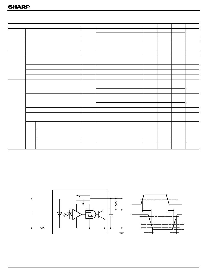
Internal connection
diagram
Voltage regulator
2. " Low " output during light emission
1. Mini-flat package
( V
iso
rms
)
data books, etc. Contact SHARP in order to obtain the latest version of the device specification sheets before using any SHARP's device.
"
"
In the absence of confirmation by device specification sheets, SHARP takes no responsibility for any defects that occur in equipment using any of SHARP's devices, shown in catalogs,
( Ta = 25°C)
s
Absolute Maximum Ratings
(Input Side)
6
°
1
3
6
Amp.
5
4
Compact, Surface Mount Type
OPIC Photocoupler
Forward current
Reverse voltage
Power dissipation
Supply voltage
High level output voltege
Low level output current
Power dissipation
Parameter
( Unit : mm)
*1 AC for 1 minute, 40 to 60% RH
*2 For 10 seconds
Soldering temperature
0.2mm or more
Soldering area
4. TTL and LSTTL compatible output
5. Recognized by UL(No.E64380)
Model No.
Package specifications
Diameter of reel
Tape width
PC400
370mm
12mm
PC400T
Taping package
( Net: 750pcs. )
178mm
12mm
PC400Z
Sleeve package
( Net: 100pcs. )
-
-
: 3 750V
Taping package
( Net:3 000pcs. )
V
rms
3 750
C0.4
An OPIC consists of a light-detecting element and signal-
processing circuit integrated onto a single chip.
* " OPIC " ( Optical IC ) is a trademark of the SHARP Corporation.
4.4
±
0.2
1.27
±
0.25
2.54
±
0.25
0.4
±
0.1
3.6
±
0.3
2.6
±
0.2
0.1
±
0.1
5.3
±
0.3
0.2
±
0.05
0.5
+
0.4
-
0.2
7.0
+
0.2
-
0.7
3 Cathode
s
Electro-optical Characteristics
Forward voltage
V
F
Reverse current
I
R
Terminal capacitance
C
t
Operating supply voltage
V
CC
Low level output voltage
V
OL
High level output current
I
OH
Low level supply current
I
CCL
High level supply current
I
CCH
*3
" H
L " threshold
I
FHL
*4
" L
H " threshold
I
FLH
*5
Hysteresis
I
FLH
/I
FHL
R
ISO
t
PHL
t
PLH
Fall time
t
f
Rise time
t
r
Parameter
Symbol
Conditions
MIN.
TYP.
MAX.
Unit
Input
Output
Transfer
charac-
teristics
I
F
I
F
Ta = 25°C, V
R
= 3V
Ta = 25°C, V = 0
f = 1kHz
I
OL
CC
= 5V
I
F
V
CC
= V
O
= 15V, I
F
= 0
V
CC
= 5V, I
F
V
CC
= 5V, I
F
= 0
Ta = 25°C,V
CC
= 5V
R
L
= 280
V
CC
= 5V,R
L
= 280
Ta = 25°C,V
CC
= 5V
R
L
= 280
V
CC
= 5V,R
L
= 280
V
CC
= 5V,R
L
= 280
*6
Response
- 1.1 1.4
V
0.7 1.0 -
- - 10
µ
A
- 30
250 pF
3 -
15
V
- 0.2 0.4 V
- -
100
µ
A
- 2.5 5.0 mA
- 1.0 5.0 mA
- 1.1 2.0
mA
- -
4.0
0.4 0.8 -
mA
0.3 - -
0.5 0.7 0.9
5 x 10
10
10
11
-
- 1 3
µ
s
- 2 6
- 0.05
0.5
- 0.1 0.5
PC400
*3 I
FHL
represents forward current when output gose from high to low.
*4 I
FLH
represents forward current when output goes from low to high.
*5 Hysteresis stands for I
FLH
/I
FHL
.
*6 Test circuit for response time is shown below.
time
time
47
V
IN
Amp
Voltage
regulator
5V
280
V
o
0.1
µ
F
V
IN
V
o
t
t
PLH
t
f
t
f
50
%
V
OH
90
%
1.5V
10
%
V
OL
t
r
=
t
f
=
0.01
µ
S
Z
o
=
50
Isolation resistance
input current
input current
time
Ta = 25°C, DC500V
Ta = 25°C
V
= 5V,I = 4 mA
CC
F
R = 280
L
40 to 60% RH
( Ta = 0 to + 70°C unless otherwise specified )
= 4mA
= 0.3mA
= 16mA, V
= 4mA
= 4mA
" H
L " propagation delay
" L
H " propagation delay
PHL
0
200
100
150
100
50
0
25
50
75
130
85
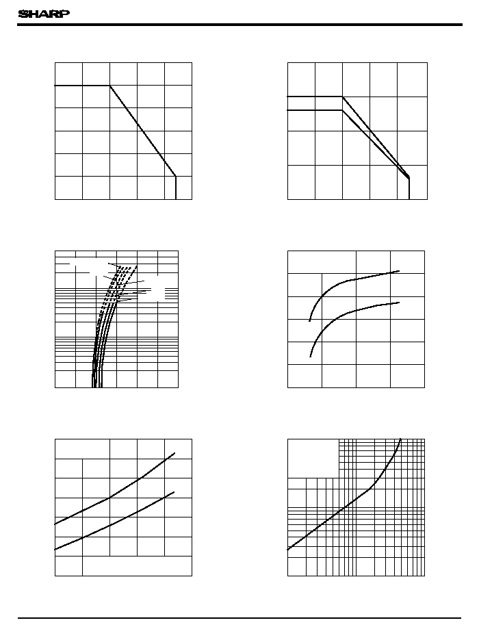
Fig. 2 Power Dissipation vs.
Ambient Temperature
Ambient temperature T
a
(°C)
Power dissipation P
O
, P
tot
(
mW
)
10
20
60
50
40
30
0
- 25
0
25
50
75
100
85
Fig. 1 Forward Current vs.
Ambient Temperature
F
(
mA
)
Ambient temperature T
a
(°C)
0.2
Relative threshold input current
0.4
0.6
1.4
5
10
20
0
15
1.2
1.0
0.8
Supply voltage V
CC
(V)
50°C
25°C
0°C
0
1
2
5
10
20
50
100
200
500
0.5
1.0
1.5
2.0
2.5
3.0
F
(
mA
)
Fig. 3 Forward Current vs.
Forward Voltage
Forward voltage V
F
(V)
- 25°C
Fig. 4 Relative Threshold Input Current vs.
Supply Voltage
0.2
0.4
Relative threshold input current
0.6
0.8
1.6
0
25
50
100
- 25
75
1.4
1.2
1.0
Ambient temperature T
a
(°C)
0.01
1
0.02
0.05
0.1
1.0
2
5
10
100
50
20
0.2
0.5
Low level output voltage V
OL
(
V
)
Low level output current I
OL
( mA )
Fig. 5 Relative Threshold Input Current vs.
Ambient Temperature
PC400
Fig. 6 Low Level Output Voltage vs.
Low Level Output Current
Forward current I
Forward current I
- 25
P
tot
P
O
I
FHL
I
FLH
T
a
= 25°C
I
FHL
= 1 at V
CC
= 5V
T
a
= 75°C
I
FHL
I
FLH
V
CC
= 5V
I
FHL
= 1 at T
a
= 25°C
V
CC
= 5V
I
F
= 4mA
T
a
= 25°C
0.2
0.3
0.5
- 25
0
25
50
100
0.1
0
0.4
75
16mA
5mA
Low level output voltage V
OL
(
V
)
Ambient temperature T
a
(°C)
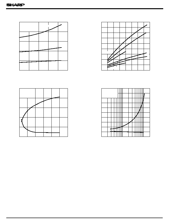
Fig. 7 Low Level Output Voltage vs.
Ambient Temperature
PC400
0
Supply current Icc
(
mA
)
1
2
9
5
9
17
1
13
5
4
3
6
7
8
11
15
7
3
25°C
85°C
25°C
85°C
Supply Voltage
Supply voltage V
CC
(V)
0
1
2
3
4
5
10
20
30
40
60
0
50
(
µ
s
)
Forward Current
0
0.1
0.1
0.2
0.3
0.4
0.5
0.2
0.5
1
2
5
10
20
Rise time,fall time
(
µ
s
)
L
( k
)
V
CC
= 5V
T
a
= 25°C
I
F
= 4mA
t
r
t
f
Forward current I
F
( mA )
Propagation delay time
- 25°C
Fig.10 Rise Time, Fall Time vs.
Fig. 9 Propagation Delay Time vs.
Fig. 8 Supply Current vs.
s
Preautions for Use
GND near the device in order to stabilize power supply line.
( 2) Handle this product the same as with other integrated circuits against static electricity.
( 3) As for other general cautions, refer to the chapter "Precautions for Use "
( 1) It is recommended that a by-pass capacitor of more than 0.01
µ
F be added between V
CC
and
V
CC
= 5V
I
F
= 4mA
I
OL
= 30mA
T
a
= - 25°C
I
CCL
I
CCL
I
CCH
I
CCH
t
PHL
t
PLH
V
CC
= 5V
R
L
= 280
T
a
= 25°C
Load resistance R
Load Resistance