PC1231
X
NSZ Series
PC1231
X
NSZ Series
s
Rank Table
s
Absolute Maximum Ratings
s
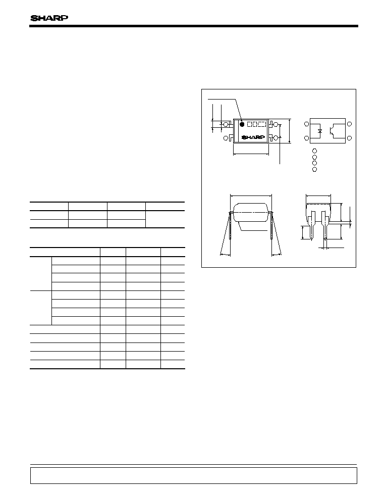
Outline Dimensions
(Unit : mm)
Low Input Current Type
Long Creepage Distance
Photocoupler
1. Home appliances
2. Programmable controllers
s
Features
s
Applications
1. Low input current type (I
F
=
0.5mA)
2. High resistance to noise due to high common mode rejection
voltage (CMR:MIN. 10kV/
µ
s)
3. Long creepage distance type
4. Standard 4-pin dual-in-line package
5. Isolation voltage (Viso : 5kVrms)
Model No.
Rank mark
Ic (mA)
Conditions
PC12310NSZ
PC12311NSZ
A or no mark
A
0.25 to 2.0
0.5 to 1.25
I
F
=
0.5mA
V
CE
=
5V
T
a
=
25
°
C
*1 Pulse width
<=
100
µ
s, Duty ratio
=
0.001
*2 40 to 60%RH, AC for 1 minute, f
=
60Hz
*3 For 10s
Parameter
Symbol
Rating
Unit
Forward current
Peak forward current
I
F
I
FM
10
200
mA
mA
mA
Reverse voltage
Input
Output
V
R
6
V
V
Power dissipation
Collector-emitter voltage
P
15
Collector power dissipation
Collector current
Total power dissipation
150
70
50
mW
mW
mW
P
tot
I
C
P
C
V
CEO
V
Emitter-collector voltage
6
V
ECO
V
iso
kV
rms
170
Operating temperature
T
opr
-
55 to
+
125
-
30 to
+
100
°
C
°
C
Storage temperature
Isolation voltage
T
stg
*2
*3
*1
Soldering temperature
T
sol
260
5
°
C
(Ta
=
25
°
C)
1 2 3 1
4.58
±
0.5
0.6
±
0.2
1.2
±
0.3
2.54
±
0.25
6.5
±
0.5
7.62
±
0.3
4.58
±
0.5
3.5
±
0.5
3.0
±
0.5
2.7
±
0.5
0.5
TYP.
Anode mark
0.5
±
0.1
: 0 to 13
°
Epoxy resin
1
2
4
3
Internal connection
diagram
1
2
3
4
Anode
Anode
Cathode
Emitter
Collector
1
2
4
3
Notice
In the absence of confirmation by device specification sheets, SHARP takes no responsibility for any defects that may occur in equipment using any SHARP
devices shown in catalogs, data books, etc. Contact SHARP in order to obtain the latest device specification sheets before using any SHARP device.
Internet
Internet address for Electronic Components Group http://www.sharp.co.jp/ecg/
PC1231
X
NSZ Series
s
Electro-optical Characteristics
Fig.1 Test Circuit for Common Mode Rejection Voltage
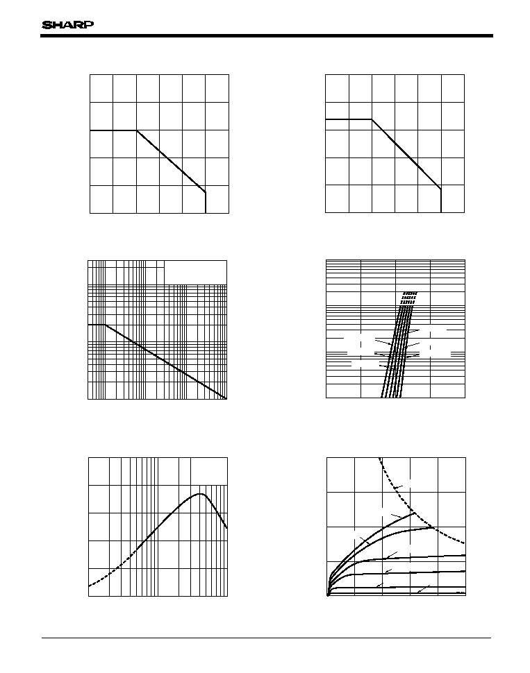
Fig.2 Forward Current vs. Ambient
Temperature
Parameter
Symbol
MIN.
TYP.
MAX.
Unit
Forward voltage
Reverse current
Collector current
Isolation resistance
Floating capacitance
Response time
Common mode rejection voltage
Terminal capacitance
Collector dark current
Emitter-collector breakdown voltage
Collector-emitter breakdown voltage
Collector-emitter saturation voltage
Rise time
Fall time
V
F
I
R
C
t
I
CEO
BV
CEO
BV
ECO
R
ISO
C
f
I
C
V
CE (sat)
tr
tf
CMR
Conditions
I
F
=
10mA
I
F
=
0.5mA, V
CE
=
5V
I
F
=
10mA, I
C
=
1mA
V
R
=
4V
V
=
0, f
=
1kHz
V
CE
=
50V, I
F
=
0
I
C
=0.1mA, I
F
=0
I
E
=10
µ
A, I
F
=0
DC500V, 40 to 60%RH
V
=
0, f
=
1MHz
V
CE
=
2V, I
C
=
2mA, R
L
=
100
Ta
=
25
°
C, R
L
=
470
,
V
CM
=
1.5kV (peak),
I
F
=
0mA, V
CC
=
9V, Vnp
=
100mV
1.4
V
-
-
-
-
70
6
0.25
5
×
10
10
10
11
30
1.2
-
-
2.0
250
-
0.6
1.0
-
4
18
-
3
18
100
-
-
10
-
10
-
-
V
-
-
-
V
V
-
0.2
-
µ
A
µ
s
µ
s
kV/
µ
s
mA
pF
pF
nA
(Ta
=
25
°
C)
I
n
p
u
t
O
u
t
p
u
t
T
r
a
n
s
f
e
r
c
h
a
r
a
c
t
e
r
i
s
t
i
c
s
*1 Refer to Fig. 1
*1
V
CM
V
cp
V
np
V
O
(dV/d
t
)
1)
R
L
V
np
V
CC
V
CM
V
CM :
High wave
pulse
R
L
=
470
V
CC
=
9V
1) V
cp
: Voltage which is generated by displacement current in floating
capacitance between primary and secondary side.
(V
cp
Nearly
=
dV/d
t
×
C
f
×
R
L
)
F
o
r
w
a
r
d
c
u
r
r
e
n
t
I
F
(
m
A
)
Ambient temperature T
a
(
°
C)
0
10
5
-
30
0
25
50
75
100
125
Fig.3 Diode Power Dissipation vs. Ambient
Temperature
D
i
o
d
e
p
o
w
e
r
d
i
s
s
i
p
a
t
i
o
n
P
(
m
W
)
Ambient temperature T
a
(
°
C)
0
15
10
5
-
30
0
25
50
75
100
125
PC1231
X
NSZ Series
Fig.6 Peak Forward Current vs. Duty Ratio
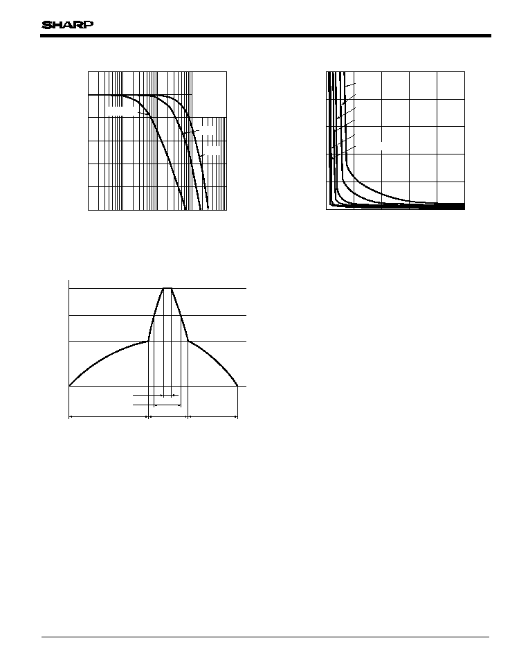
Fig.9 Collector Current vs. Collector-emitter
Voltage
Fig.7 Forward Current vs. Forward Voltage
P
e
a
k
f
o
r
w
a
r
d
c
u
r
r
e
n
t
I
F
M
(
m
A
)
Duty ratio
10
1000
100
10
-
2
10
-
3
10
-
1
2
2
2
5
5
5
5
1
2000
200
20
500
50
Pulse width
<=
100
µ
s
T
a
=
25
°
C
F
o
r
w
a
r
d
c
u
r
r
e
n
t
I
F
(
m
A
)
0.1
1
10
100
0
0.5
1.0
1.5
2.0
Forward voltage V
F
(V)
T
a
=
25
°
C
T
a
=
75
°
C
T
a
=
100
°
C
T
a
=
50
°
C
T
a
=
0
°
C
T
a
=-
25
°
C
C
o
l
l
e
c
t
o
r
c
u
r
r
e
n
t
I
C
(
m
A
)
Collector-emitter voltage V
CE
(V)
0
40
0
2
4
6
8
10
T
a
=
25
°
C
30
20
10
P
C
(MAX.)
I
F
=
7mA
I
F
=
5mA
I
F
=
3mA
I
F
=
2mA
I
F
=
1mA
I
F
=
0.5mA
Fig.5 Total Power Dissipation vs. Ambient
Temperature
Fig.4 Collector Power Dissipation vs.
Ambient Temperature
T
o
t
a
l
p
o
w
e
r
d
i
s
s
i
p
a
t
i
o
n
P
t
o
t
(
m
W
)
Ambient temperature T
a
(
°
C)
0
200
150
170
100
50
-
30
0
25
50
75
100
125
C
o
l
l
e
c
t
o
r
p
o
w
e
r
d
i
s
s
i
p
a
t
i
o
n
P
C
(
m
W
)
Ambient temperature T
a
(
°
C)
0
200
150
100
50
-
30
0
25
50
75
100
125
Fig.8 Current Transfer Ratio vs. Forward
Current
C
u
r
r
e
n
t
t
r
a
n
s
f
e
r
r
a
t
i
o
C
T
R
(
%
)
Forward current I
F
(mA)
0.1
1
10
0
500
400
300
200
100
V
CE
=
5V
T
a
=
25
°
C
PC1231
X
NSZ Series
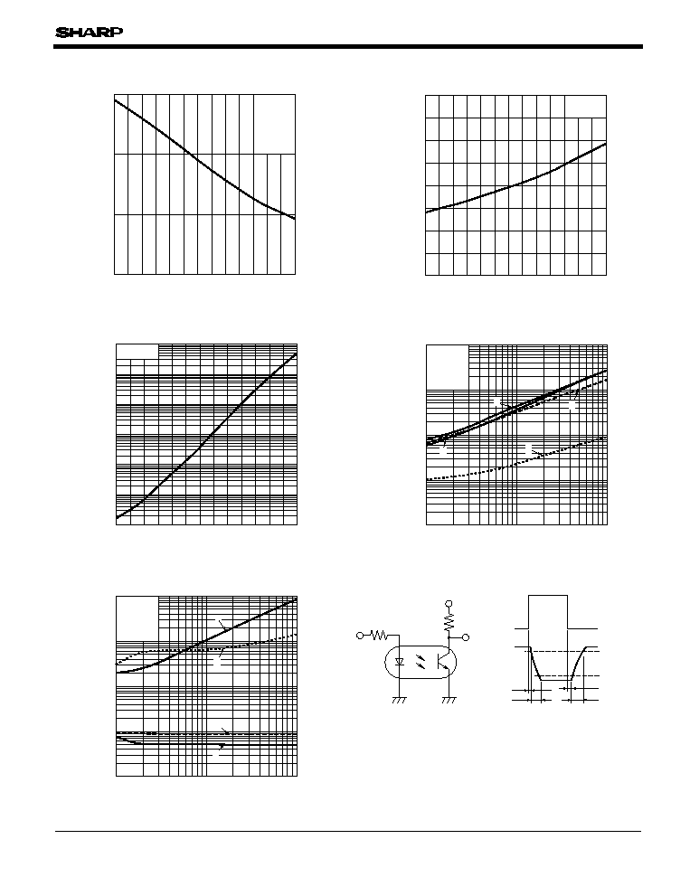
Fig.10 Relative Current Transfer Ratio vs.
Ambient Temperature
Fig.13 Response Time vs. Load Resistance
R
e
l
a
t
i
v
e
c
u
r
r
e
n
t
t
r
a
n
s
f
e
r
r
a
t
i
o
(
%
)
Ambient temperature T
a
(
°
C)
-
30
100
90
80
70
60
50
40
30
20
10
0
-
10
-
20
V
CE
=
5V
I
F
=
0.5mA
0
150
100
50
R
e
s
p
o
n
s
e
t
i
m
e
(
µ
s
)
0.1
1000
0.1
1
10
Load resistance R
L
(k
)
V
CE
=
2V
I
C
=
2mA
T
a
=
25
°
C
t
f
t
r
t
d
t
s
100
10
1
Fig.11 Collector - emitter Saturation Voltage
vs. Ambient Temperature
C
o
l
l
e
c
t
o
r
-
e
m
i
t
t
e
r
s
a
t
u
r
a
t
i
o
n
v
o
l
t
a
g
e
V
C
E
(
s
a
t
)
(
V
)
Ambient temperature T
a
(
°
C)
0
0.16
0.14
0.12
0.10
0.08
0.06
0.04
0.02
I
F
=
10mA
I
C
=
1mA
-
30
100
90
80
70
60
50
40
30
20
10
0
-
10
-
20
Fig.12 Collector Dark Current vs. Ambient
Temperature
Ambient temperature T
a
(
°
C)
-
30
100
90
80
70
60
50
40
30
20
10
0
-
10
-
20
V
CE
=
50V
10
-
11
10
-
5
10
-
6
10
-
7
10
-
8
10
-
9
10
-
10
C
o
l
l
e
c
t
o
r
d
a
r
k
c
u
r
r
e
n
t
I
C
E
O
(
A
)
Fig.14 Response Time vs. Load Resistance
(Saturation)
R
e
s
p
o
n
s
e
t
i
m
e
(
µ
s
)
0.1
1000
1
10
100
Load resistance R
L
(k
)
V
CC
=
5V
I
F
=
16mA
T
a
=
25
°
C
t
f
t
d
t
s
100
10
1
t
r
Fig.15 Test Circuit for Response Time
10%
Input
Output
Input
Output
90%
t
s
t
d
V
CC
R
D
R
L
t
f
t
r
PC1231
X
NSZ Series
Fig.18 Reflow Soldering
25
°
C
2min
230
°
C
200
°
C
180
°
C
1min
30s
1min
10s
Only one time soldering is recommended within the temperature
profile shown below.
Fig.16 Voltage gain vs Frequency
V
o
l
t
a
g
e
g
a
i
n
A
V
(
d
B
)
-
25
5
0.1
1
10
100
1000
Frequency f (kHz)
V
CE
=
2V
I
C
=
2mA
T
a
=
25
°
C
0
-
5
-
10
-
15
-
20
R
L
=
10k
1k
100
Fig.17 Collector-emitter Saturation Voltage
vs. Forward Current
C
o
l
l
e
c
t
o
r
-
e
m
i
t
t
e
r
s
a
t
u
r
a
t
i
o
n
v
o
l
t
a
g
e
V
C
E
(
s
a
t
)
(
V
)
Forward current I
F
(mA)
0
5
0
2
4
6
8
10
T
a
=
25
°
C
4
3
2
1
I
C
=
7mA
I
C
=
5mA
I
C
=
3mA
I
C
=
2mA
I
C
=
1mA
I
C
=
0.5mA