
data books, etc. Contact SHARP in order to obtain the latest version of the device specification sheets before using any SHARP's device.
"
"
In the absence of confirmation by device specification sheets, SHARP takes no responsibility for any defects that occur in equipment using any of SHARP's devices, shown in catalogs,
3. High collector-emitter voltage
2. OA equipment
PC123/PC123F
PC123/PC123F
s
Features
(Unit : mm )
s
Applications
(Ta = 25°C )
Creepage distance
Space distance
PC123
PC123F
8mm or more
8mm or more
Symbol
Ratings
Unit
Input
I
F
50
mA
I
FM
1
A
V
R
6
V
P
70
mW
Output
V
CEO
70
V
V
ECO
6
V
Collector current
I
C
50
mA
P
C
150
mW
V
iso
5
Operating temperature
T
opr
- 30 to + 100
°C
T
stg
- 55 to + 125
°C
P
tot
200
mW
T
sol
260
°C
Reverse voltage
Collector-emitter voltage
Anode mark
Internal connection diagram
1
2
4
3
1 Anode
2 Cathode
3 Emitter
4 Collector
1
2
4
3
Epoxy resin
PC123
PC123
3
4
2
1
4 Collector
3 Emitter
2 Cathode
1 Anode
3
4
2
1
diagram
Internal connection
Anode mark
Epoxy resin
s
Outline Dimensions
European Safety Standard
Approved Type Long Creepage
Distance Photocoupler
1. Conform to European Safety Standard
2. Internal isolation distance : 0.4mm or more
( V
CEO
: 70V)
1. Power supplies
s
Absolute Maximum Ratings
Parameter
Forward current
*1
Peak forward current
Power dissipation
Total power dissipation
*2
Isolation voltage
Storage temperature
*3
Soldering temperature
*2 AC for 1 minute, 40 to 60% RH
*3 For 10 seconds
*1 Pulse width <= 100
µ
s, Duty ratio : 0.001
PC123
PC123F
Emitter-collector voltage
Collector power dissipation
6.4mm or more
6.4mm or more
kV
rms
1.0
±
0.1
1.2
±
0.3
6.5
±
0.3
2.54
±
0.25
4.58
±
0.3
7.62
±
0.3
4.58
±
0.3
0.26
±
0.1
0.5
±
0.1
3.5
±
0.5
3.05
±
0.5
3.4
±
0.5
1.2
±
0.3
1.0
±
0.1
0.5
±
0.1
0.26
±
0.1
4.58
±
0.3
7.62
±
0.3
4.58
±
0.3
6.5
±
0.3
2.54
±
0.25
2.7
MIN.
3.5
±
0.5
10.16
±
0.5
g DIN-VDE0884 approved type
( PC123Y/PC123FY )
is also available as an option.
4. Long creepage distance type
5. Recognized by UL (No. E64380)
Recognized by CSA (No. CA95323)
Approved by VDE ( DIN-VDE83601 )
Approved by BSI
Approved by SEMCO ( No. 9216212 )
Approved by DEMCO ( No. 108954 )
Approved by NEMKO ( No. 199438181 )
Approved by EI ( No. 155030 )
( BS415 No. 7087, BS7002 No. 7409 )
( Ta = 25°C)
PC123/PC123F
Parameter
Symbol
Conditions
Unit
Input
Forward voltage
V
F
I
F
= 20mA
-
1.2
1.4
V
I
R
V
R
= 4V
-
-
10
µ
A
Terminal capacitance
C
t
V = 0, f = 1kHz
-
30
250
pF
Output
Collector dark current
I
CEO
V
CE
F
= 0
-
-
100
nA
Collector-emitter breakdown voltage
BV
CEO
I
C
= 0.1mA, I
F
= 0
70
-
-
V
Emitter-collector breakdown voltage
BV
ECO
I
E
= 10
µ
A, I
F
= 0
6
-
-
V
Transfer
characte-
risitics
Collector current
I
C
I
F
= 5mA, V
CE
= 5V
2.5
-
20
mA
Collector-emitter saturation voltage
V
CE( sat )
I
F
= 20mA, I
C
= 1mA
-
0.1
0.2
V
Isolation resistance
5 x 10
10
10
11
-
Floating capacitance
C
f
V = 0, f = 1MHz
-
0.6
1.0
pF
f
c
V
CE
= 5V, I
C
= 2mA
-
80
-
kHz
Response time
Rise time
t
r
V
CE
= 2V, I
C
= 2mA
R
L
= 100
-
4
18
Fall time
t
-
3
18
s
Electro-optical Characteristics
Reverse current
Cut-off frequency
R
ISO
R
L
= 100
, - 3dB
MIN.
TYP.
MAX.
µ
s
µ
s
0
- 30
10
0
25
50
75
100
125
20
30
40
50
60
Fig. 1 Forward Current vs.
Ambient Temperature
Ambient temperature T
a
(°C)
Forward current I
F
(
mA
)
70
25
0
100
80
60
40
20
0
50
100
Fig. 2 Diode Power Dissipation vs.
Ambient Temperature
a
( °C )
- 30
f
DC500V, 40 to 60%RH
Diode power dissipation P
(
mW
)
Ambient temperature T
= 50V, I
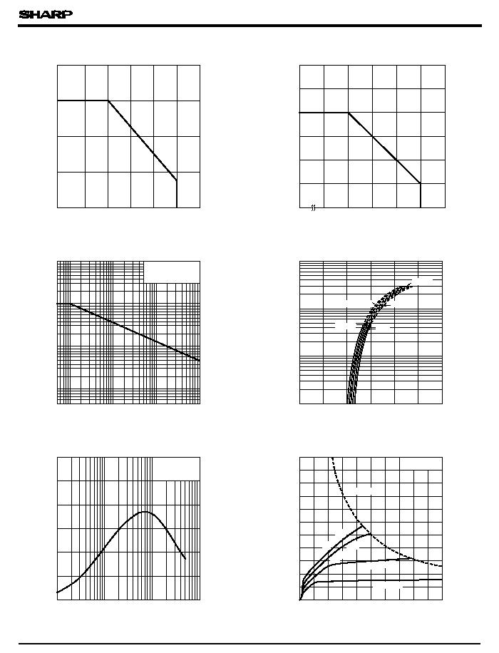
PC123/PC123F
0
0
125
100
200
50
150
25
50
75
100
Ambient Temperature
- 30
Ambient temperature T
a
(°C)
Collector power dissipation P
C
(
mW
)
Fig. 3 Collector Power Dissipation vs.
0
250
200
150
50
100
0
25
50
75
100
125
Fig. 4 Power Dissipation vs.
Ambient Temperature
- 30
Power dissipation P
tot
(
mW
)
Duty ratio
5
5
Pulse width <=100
µ
s
10
20
100
50
200
500
2
10
- 3
10
- 2
5
2
10
- 1
5
2
5
Peak forward current I
FM
(
mA
)
Fig. 5 Peak Forward Current vs. Duty Ratio
0
0.5
1.0
1.5
2.0
2.5
3.0
1
2
5
10
20
50
100
200
500
+ 25°C
- 25°C
50°C
0°C
Fig. 6 Forward Current vs.
Forward Voltage
Forward voltage V
F
(V)
T
a
Forward current I
F
(
mA
)
Forward current I
F
( mA )
Current transfer ratio CTR
(
%
)
0.1
1
10
100
0
50
100
150
200
250
300
V
CE
= 5V
T
a
= 25°C
Fig. 7 Current Transfer Ratio vs.
Forward Current
Collector-emitter voltage V
CE
(V)
0
1
2
3
4
5
6
7
8
9
10
0
6
12
18
24
30
36
42
48
54
60
T
a
= 25°C
I
F
=
30mA
I
F
=
20mA
I
F
= 10mA
I
F
= 5mA
Fig. 8 Collector Current vs. Collector-emitter
Voltage
Collector current I
C
(
mA
)
= 75°C
P
C
( MAX.)
T
a
= 25°C
Ambient temperature T
a
( °C)
1000
10000
5000
2000
1000
1
PC123/PC123F
50
0
100
150
0
25
50
75
100
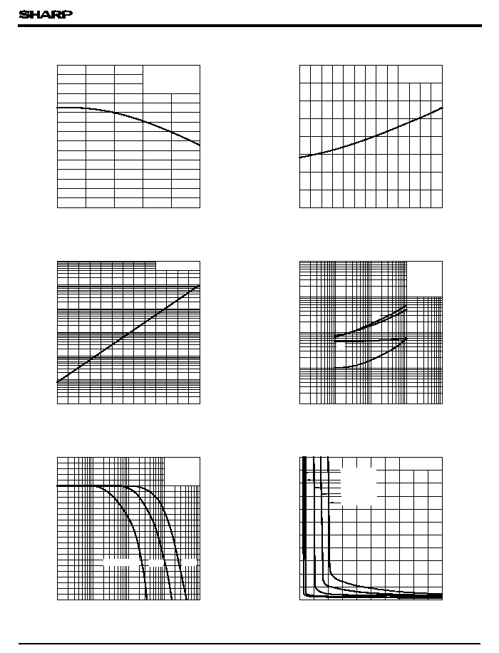
Relative current transfer ratio
(
%
)
- 30
Ambient temperature T
a
(°C)
Collector-emitter saturation voltage V
CE
( sat
)
(
V
)
- 30
0
20
40
60
80
100
0.00
0.02
0.04
0.06
0.08
0.10
0.12
0.14
0.16
I
F
= 20mA
I
c
= 1mA
Ambient temperature T
a
(°C)
Collector dark current I
CEO
(
A
)
- 30
0
20
40
60
80
100
10
- 11
5
10
- 10
5
10
- 9
5
10
- 8
5
10
- 7
5
10
- 6
5
10
- 5
V
CE
= 50V
Response time
(
µ
s
)
0.01
0.1
1
10
100
0.1
1
10
100
V
CE
= 2V
I
C
= 2mA
T
a
= 25°C
t
r
t
f
t
d
t
s
Frequency ( kHz )
Voltage gain Av
(
dB
)
0.1
10
100
- 20
1
- 15
- 10
- 5
0
5
V
CE
= 5V
I
C
= 2mA
T
a
= 25°C
R
L
= 10k
1k
100
Forward current I
F
( mA )
Collector-emitter saturation voltage V
CE
( sat
)
(
V
)
0
2
4
6
8
10
12
14
16
18
20
0
0.5
1.0
1.5
2.0
2.5
3.0
3.5
4.0
4.5
5.0
T
a
= 25°C
I
C
= 0.5mA
Fig. 9 Relative Current Transfer Ratio vs.
Ambient Temperature
Fig.10 Collector-emitter Saturation Voltage vs.
Ambient temperature
Fig.11 Collector Dark Current vs.
Ambient Temperature
Fig.12 Response Time vs.
Fig.13 Frequency Response
Fig.14 Collector-emitter Saturation Voltage vs.
Forward Currnt
I
F
= 5mA
V
CE
= 5V
Ambient temperature T
a
( °C)
1mA
3mA
7mA
5mA
1000
1000
Please refer to the chapter "Precautions for Use "
Load Resistance
Load resistance ( k
)
q