Äîêóìåíòàöèÿ è îïèñàíèÿ www.docs.chipfind.ru
In the absence of confirmation by device specification sheets, SHARP takes no responsibility for any defects that may occur in equipment using any SHARP devices shown in
catalogs, data books, etc. Contact SHARP in order to obtain the latest device specification sheets before using any SHARP device.
1
DESCRIPTION
The LR38616 is a CMOS timing generator IC
which generates timing pulses for driving 2 140 k-
pixel CCD area sensors and processing pulses.
FEATURES
· Designed for 1/2-type 2 140 k-pixel CCD area
sensors
· Frequency of driving horizontal CCD : 17.987 MHz
· Both double speed drive monitoring mode and
still mode are possible
· Two still mode types :
3 fields period and 4 fields period
· External shutter control function with serial data
input is possible
· +3 V and +4.5 V power supplies
· Package :
48-pin QFP (QFP048-P-0707) 0.5 mm pin-pitch
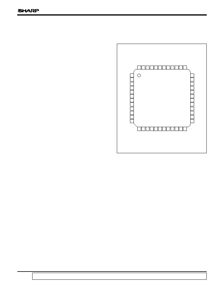
PIN CONNECTIONS
LR38616
LR38616
Timing Generator IC for
2 140 k-pixel CCDs
1
48 47 46 45 44 43 42 41 40 39
37
13 14 15 16 17 18 19 20 21 22 23 24
2
3
4
5
6
7
8
9
10
11
12
36
35
34
33
32
31
30
29
28
27
26
25
OFDC
V
1x
VH
1Ax
VH
1Bx
V
2x
V
DD3
GND
V
3x
VH
3Ax
VH
3Bx
V
4x
OFDX
ID
ED
2
ED
1
ED
0
HD
GND
V
DD3
VD
DCLK
CLK
CKO
CKI
PBLK
BCPX
CLPX
ADCK
GND
FCDS
FS
V
DD3
ACLX
RS
GND
VCON
SHTR
STMD
FR
TST
3
V
DD4
FH
2
GND
FH
1
V
DD4
TVMD
TST
2
TST
1
38
48-PIN QFP
TOP VIEW
(QFP048-P-0707)
LR38616
2
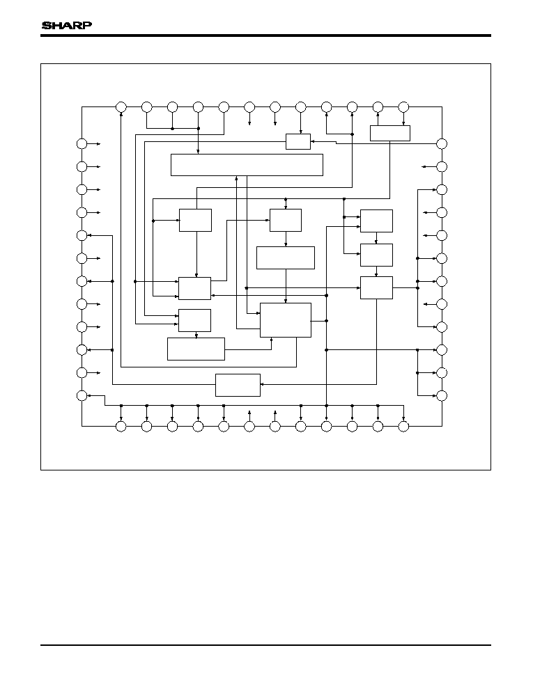
BLOCK DIAGRAM
ID
ED
2
ED
1
ED
0
HD
GND
V
DD3
VD
DCLK
CLK
CKO
CKI
36
35
34
33
32
31
30
29
28
27
26
25
VCON
GND
RS
ACLX
V
DD3
FS
FCDS
GND
ADCK
CLPX
BCPX
PBLK
OFDC
V
1X
VH
1AX
VH
1BX
V
2X
V
DD3
GND
V
3X
VH
3AX
VH
3BX
V
4X
OFDX
TST
1
TST
2
TVMD
V
DD4
FH
1
GND
FH
2
V
DD4
TST
3
FR
STMD
SHTR
1/2
1/8
GATE
OSC
DATA LATCH & SHUTTER CONTROL
RESET
RESET
RESET
1/2
GATE
H COUNTER
V COUNTER
LEVEL
SHIFTER
DECODER
13
14
15
16
17
18
19
20
21
22
23
24
1
2
3
4
5
6
7
8
9
10
11
12
48
47
46
45
44
43
42
41
40
39
38
37
3
LR38616
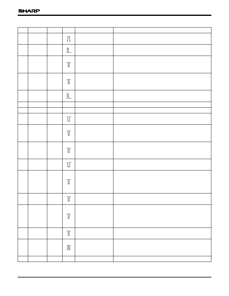
PIN NO. SYMBOL
I/O
POLARITY
PIN NAME
DESCRIPTION
1
OFDC
O3
Control pulse output
for OFD voltage
A pulse to control OFD voltage.
2
V
1X
O3
Vertical transfer
pulse output 1
A vertical transfer pulse for CCD.
Connect to V
1X
pin of vertical driver IC.
3
VH
1AX
O3
Readout pulse
output 1A
A pulse that transfers the charge of the photo-diode to
the vertical shift register.
Connect to VH
1AX
pin of vertical driver IC.
4
VH
1BX
O3
Readout pulse
output 1B
A pulse that transfers the charge of the photo-diode to
the vertical shift register.
Connect to VH
1BX
pin of vertical driver IC.
5
V
2X
O3
Vertical transfer
pulse output 2
A vertical transfer pulse for CCD.
Connect to V
2X
pin of vertical driver IC.
6
V
DD3
Power supply
Supply of +3.3 V power.
A grounding pin.
Ground
GND
7
9
VH
3AX
O3
Readout pulse
output 3A
A pulse that transfers the charge of the photo-diode to
the vertical shift register.
Connect to VH
3AX
pin of vertical driver IC.
8
V
3X
O3
Vertical transfer
pulse output 3
A vertical transfer pulse for CCD.
Connect to V
3X
pin of vertical driver IC.
A pulse that transfers the charge of the photo-diode to
the vertical shift register.
Connect to VH
3BX
pin of vertical driver IC.
Readout pulse
output 3B
O3
VH
3BX
10
11
V
4X
O3
Vertical transfer
pulse output 4
A vertical transfer pulse for CCD.
Connect to V
4X
pin of vertical driver IC.
A pulse that sweeps the charge of the photo-diode for
the electronic shutter. Connect to OFD pin of CCD
through the vertical driver IC and DC offset circuit.
Held at H level at normal mode.
OFD pulse output
O3
OFDX
12
13
PBLK
O3
Pre-blanking pulse
output
A pulse that corresponds to the cease period of the
horizontal transfer pulse.
A pulse to clamp the optical black signal.
This pulse stays high during the absence of
effective pixels within the vertical blanking or the period
of sweep-out signal.
Optical black clamp
pulse output
O3
BCPX
14
15
CLPX
O3
Clamp pulse output
A pulse to clamp the dummy outputs of CCD signal.
This pulse stays high during the sweep-out period.
An output pin for AD converter.
The output phase of ADCK is selected by serial data
step by 90°.
AD clock output
O6MA3
ADCK
16
17
GND
Ground
A grounding pin.
PIN DESCRIPTION
4
LR38616
PIN NO. SYMBOL
I/O
POLARITY
PIN NAME
DESCRIPTION
20
V
DD3
Power supply
Supply of +3.3 V power.
An input pin for resetting all internal circuits at power on.
Connect to V
DD
through the diode and GND through the
capacitor.
All clear input
ICU3
ACLX
21
A grounding pin.
Ground
GND
23
22
RS
O6MA3
S/H pulse output
A pulse to sample-hold the signal.
The output phase of RS is selected by serial data.
24
VCON
ICU3
VD control input
An input pin to control internal vertical clock for long
shutter speed.
H level or open
: VD
L level
: VD is masked by the pulse which
is latched at the rising edge of VD.
It's necessary to be set SMD = high and number of the
fields data n 2 in serial data control at VCON operation.
18
FCDS
O6MA3
CDS pulse output 1
A pulse to clamp the feed-through level from CCD.
The output phase of FCDS is selected by serial data.
A pulse to sample-hold the signal from CCD.
The output phase of FS is selected by serial data.
CDS pulse output 2
O6MA3
FS
19
An input pin for reference clock oscillation.
The frequency is 35.874 MHz.
Clock input
OSCI3
CKI
25
26
CKO
OSCO3
Clock output
An output pin for reference clock oscillation.
The output is the inverse of CKI (pin 25).
An output pin to generate HD and VD pulses.
The frequency is 17.937 MHz.
Clock output
O6MA3
CLK
27
28
DCLK
O6MA3
Clock output
An output pin for DSP IC. The frequency is 17.937 MHz.
The output phase of DCLK is selected by serial data
step by 90°.
An input pin for reference of vertical pulse.
The length of low level is 9H.
The period is following :
Still mode
: 656H
Monitoring mode
: 262.5H
Vertical reference
pulse input
IC3
VD
29
30
V
DD3
Power supply
Supply of +3.3 V power.
A grounding pin.
Ground
GND
31
32
HD
IC3
Horizontal drive
pulse input
An input pin for reference of horizontal pulse.
Connect to HD pin of DSP IC.
An input pin for the strobe pulse, to control the functions
of LR38616. For details, see
"Serial Data Control"
.
Strobe pulse input
ICSU3
ED
0
33
34
ED
1
ICSU3
Shift register clock
input
An input pin for the clock of the shift register, to control
the functions of LR38616. For details, see
"Serial Data
Control"
.
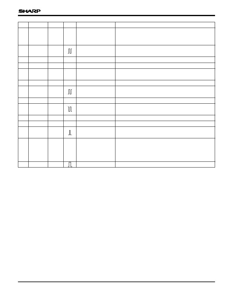
5
LR38616
PIN NO. SYMBOL
I/O
POLARITY
PIN NAME
DESCRIPTION
A test pin. Set open or to L level in the normal mode.
Test pin 1
ICD4
TST
1
37
Supply of +4.5 V power.
Power supply
V
DD4
40
O6MA43
41
FH
1
Horizontal transfer
pulse output 1
A horizontal transfer pulse for CCD.
Connect to Ø
H1
pin of CCD.
35
ED
2
ICSU3
Shift register data
input
An input pin for the data of the shift register, to control
the functions of LR38616. For details, see
"Serial Data
Control"
.
The pulse is used in color separator.
The signal switches between high and low at every line.
Line index pulse
output
O3
ID
36
38
TST
2
ICD4
Test pin 2
A test pin. Set open or to L level in the normal mode.
An input pin for TV mode selection.
TV mode selection
input
ICD4
TVMD
39
A grounding pin.
Ground
GND
42
O6MA43
43
FH
2
Horizontal transfer
pulse output 2
A horizontal transfer pulse for CCD.
Connect to Ø
H2
pin of CCD.
Supply of +4.5 V power.
Power supply
V
DD4
44
ICD4
45
TST
3
Test pin 3
A test pin. Set open or to L level in the normal mode.
A pulse to reset the charge of output circuit.
The output phase of FR is selected by serial data.
Reset pulse output
FR
46
O6MA43
ICU4
47
STMD
Drive mode selection
input
An input pin for setting the repetition to take the still
picture.
H level or open
: 4 fields period
L level
: 3 fields period
A trigger pulse for effective signal period.
Trigger output
SHTR
48
O3
IC3
: Input pin (CMOS level)
ICU3
: Input pin (CMOS level with pull-up resistor)
ICSU3
: Input pin (CMOS level with schmitt-trigger)
ICU4
: Input pin (CMOS level with pull-up resistor)
ICD4
: Input pin (CMOS level with pull-down resistor)
O3
: Output pin (output high level is V
DD3
.)
O6MA3
: Output pin (output high level is V
DD3
.)
O6MA43 : Output pin (output high level is V
DD4
.)
OSCI3
: Input pin for oscillation
OSCO3
: Output pin for oscillation
Document Outline