/home/web/htmldatasheet/RUSSIAN/html/sharp/177825

P
RODUCT
S
PECIFICATIONS
Mobile Liquid Crystal Displays Group
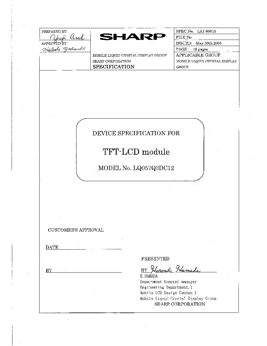
LQ057Q3DC12
TFT-LCD Module
Spec. Issue Date:
May 30, 2005
No: LA1-
05016
LCP-0
5016-1
NOTICE
This publication is the proprietary of SHARP and is copyrighted, with all rights reserved. Under the copyright laws, no part of
this publication may be reproduced or transmitted in any form or by any means, electronic or mechanical for any purpose, in
whole or in part, without the express written permission of SHARP Express written permission is also required before any use of
this publication may be made by a third party.
The application circuit examples in this publication are provided to explain the representative applications of SHARP's devices
and are not intended to guarantee any circuit design or permit any industrial property right or other rights to be executed. SHARP
takes no responsibility for any problems related to any industrial property right or a third party resulting from the use of
SHARP's devices, except for those resulting directly from device manufacturing processes.
In the absence of confirmation by device specification sheets, SHARP takes no responsibility for any defects that occur in
equipment using any of SHARP's devices, shown in catalogs, data books, etc. Contact SHARP in order to obtain the latest
device specification sheets before using any SHARP's device.
SHARP reserves the right to make changes in the specifications, characteristics, data, materials, structures and other contents
described herein at any time without notice in order to improve design or reliability. Contact SHARP in order to obtain the latest
specification sheets before using any SHARP's device. Manufacturing locations are also subject to change without notice.
Observe the following points when using any device in this publication. SHARP takes no responsibility for damage caused by
improper use of the devices.
The appropriate design measures should be taken to ensure reliability and safety when SHARP's devices are used for equipment
such as:
· Transportation control and safety equipment (i.e., aircraft, trains, automobiles, etc.)
· Traffic signals
· Gas leakage sensor breakers
· Alarm equipment
· Various safety devices etc.
SHARP's devices shall not be used for equipment that requires extremely high level of reliability, such as:
· Military and space applications
· Nuclear power control equipment
· Medical equipment for life support
Contact a SHARP representative, in advance, when intending to use SHARP's devices for any "specific" applications other than
those recommended by SHARP.
Contact and consult with a SHARP representative if there are any questions about the contents of this publication.
LA1-05016-2
1. Application
This specification applies to color TFT-LCD module, LQ057Q3DC12.
2. Summary and Features
This module is a color active matrix LCD module incorporating amorphous silicon TFT (Thin Film
Transistor). It is composed of a color TFT-LCD panel, driver ICs, control circuit (PWB), FPC, front
and back polarizer, sealed case, backlight unit. Graphics and texts can be displayed on a 320×RGB×
240 dots panel with 262,144 colors by suitable control supplying from the outside.
It isn't composed DC/AC inverter for a backlight drive.
The input of QVGA and VGA signal is possible.
Wide Viewing Angle technology is adopted. (The most suitable viewing angle is in the 12
o'clock direction.)
By adopting an active matrix drive, a picture with high contrast is realized.
Reflection due to external light is minimized through the use of a low reflection black matrix .
A thin, light and compact module is accomplished through the use of COG mounting
technology.
Through the use of high color purity color filter and TN-normally white mode excelled in
color reproducibility, an image with highly natural color reproduction is realized.
High viewing angle and high brightness (500cd/m2).
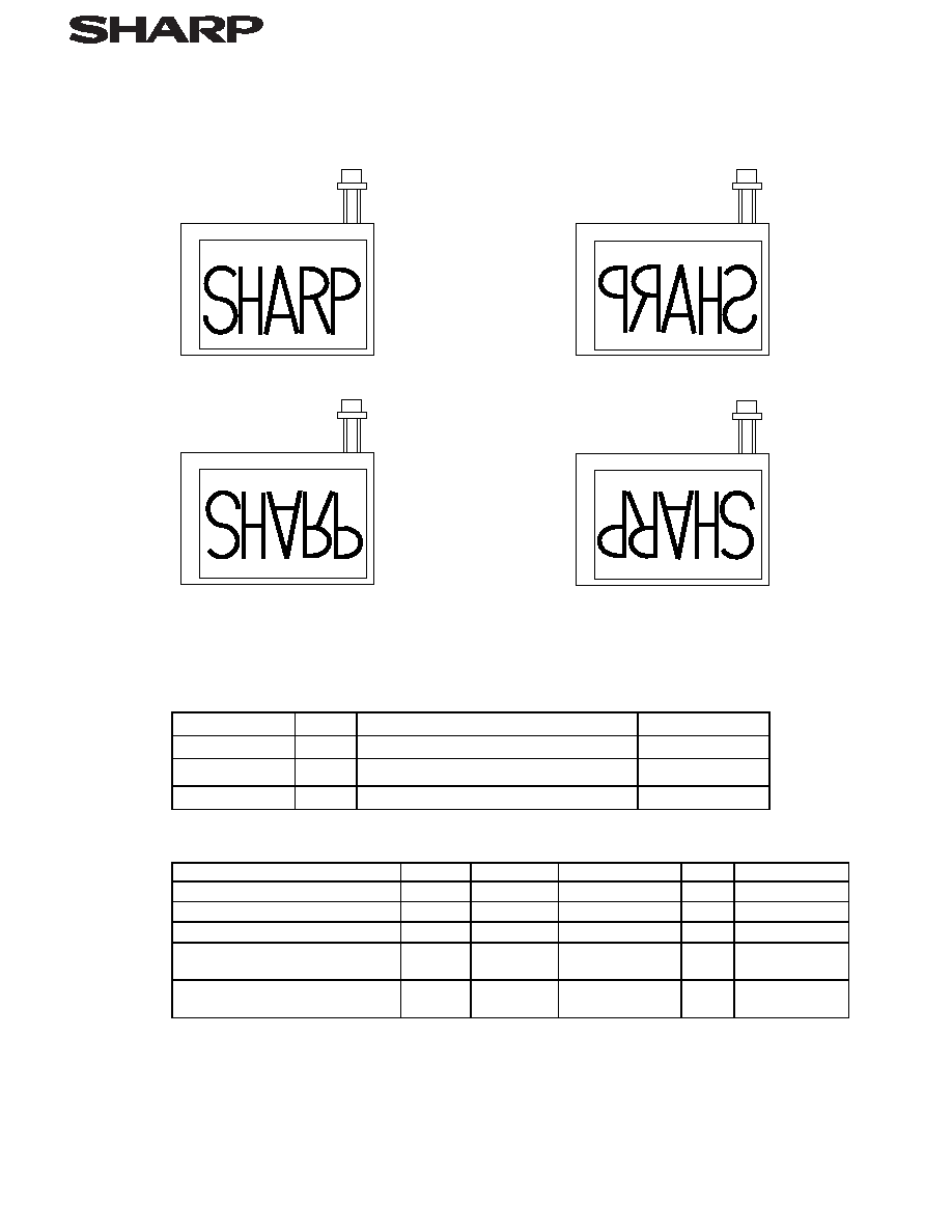
An inverted video display in the vertical / horizontal directions is possible.
This module is adapted to RoHS compliance.
3. Mechanical specifications
table 3-1
Parameter Specifications
Units
Screen size
14.4 (5.7 inch) diagonal
cm
Active area
115.2 (H) × 86.4 (V)
mm
Display format
320(H)×240(V)
pixels
(1 pixel = R + G + B dots)
Dot pitch
0.360 (H) × 0.360 ()
mm
Pixel configuration
R,G,B Stripe configuration
Display mode
Normally white
Outline dimension
Note1-1
144.0 (W)×104.6 (H)×13.0(D)
mm
Mass
220±20
Surface treatment
(Surface hardness)
Hard coat (3H)
Note 1-1
A connector of backlight is excepted.
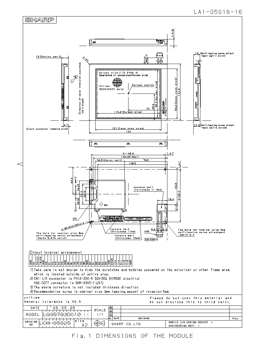
A figure of outline dimension is shown in Fig. 1.
LA1-05016-3
. Input terminal
4-1. TFT-LCD panel driving part
CN1 Used connector: FH12-33S-0.5SH(55) (HIROSE ELECTRIC C0.,LTD.)
Table 4-1 Functional table of CN1 terminals
Pin No. Symbol
Description Polarity
GND
ground
CK
Clock signal for sampling each data signal
Hsync
Horizontal synchronous signal
Negative
Vsync
Vertical synchronous signal
Negative
GND
ground
R0
RED data signal(LSB)
R1
RED data signal
R2
RED data signal
R3
RED data signal
R4
RED data signal
R5
RED data signal(MSB)
GND
ground
G0
GREEN data signal(LSB)
G1
GREEN data signal
G2
GREEN data signal
G3
GREEN data signal
G4
GREEN data signal
G5
GREEN data signal(MSB)
GND
ground
B0
BLUE data signal(LSB)
B1
BLUE data signal
B2
BLUE data signal
B3
BLUE data signal
B4
BLUE data signal
B5
BLUE data signal(MSB)
GND
ground
ENAB
Signal to settle the horizontal display positionNote4-1
Positive
Vcc
+3.3V power supply
Vcc
+3.3V power supply
R/L
Selection signal for horizontal scanning directionNote4-2
("L" : Normally , "H" : Right-and-Left reversal)
U/D
Selection signal for vertical scanning directionNote4-2
("H" : Normally , "L" : Up-and-Down reversal)
V/Q
Selection signal for VGA or QVGA
("H" : VGA , "L" : QVGA)
GND
ground
LA1-05016-4
Note 4-1 The horizontal display start timing is settled in accordance with a rising timing of
ENAB signal. In case ENAB is fixed "Low", the horizontal start timing is determined as
described in Fig7. Don't keep ENAB "High" during operation.
Note 4-2
R/L = LU/D = H R/L = HU/D = H
R/L = LU/D = L R/L = HU/D = L
4-2. Backlight fluorescent tube driving part
CN2 Used connector BHR-03VS-1 (JST Co. , Ltd.)
Suitable connector SM02(8.0)B-BHS-1N-TB (JST Co. , Ltd.)
Table 4-2 Functional table of CN2 terminals
Terminal
No.
symbol function
Color of FL cable
1 V
LOW
input
terminal (Low Voltage Side)
White
2 NC
Non connection
-
3 V
HIGH
input
terminal (High Voltage Side)
Red
5. Absolute maximum ratings
Table 5-1
Parameter Symbol
Condition
Ratings
Unit
Note
Input voltage
V
I
Ta=25
-
0.3 6.0V
V
Note 5-1
+3.3V power supply voltage
cc Ta=25 0
+.0
Storage temperature
stg --
-
30 80
Note 5-2,3
Operating temperature
Panel surface temperature
opr1 --
-
10 70
Note5-2,3,4
Operating temperature
Ambient temperature
opr2 --
-
10 +70
Note 5-5
Note 5-1 CK,
R0R5, G0G5, B0B5, Hsync, Vsync, ENAB, R/L, U/D, V/Q
Note 5-2
This rating applies to all parts of the module and should not be exceeded.
Note 5-3
Maximum wet-bulb temperature is less than 39. Condensation of dew must be
avoided as electrical current leaks will occur, causing a degradation of performance
specifications.
Note 5-4
The operating temperature only guarantees operation of the circuit. For contrast,
speed response, and other factors related to display quality, judgment is done using the
ambient temperature Ta =25.
Note 5-5
Ambient temperature when the backlight is lit (reference value).
LA1-05016-5
6. Electrical characteristics
6-1. TFT-LCD panel driving section
Table 6-1 Ta=25
Parameter Symbol
Unit Remarks
+3.3V Supply
voltage
Vcc +3.0 +3.3 +3.6 V
Note 6-1
power suply Current dissipation
Icc
-
130
160
mA Note 6-2
Permissive input ripple
V
RF
-
-
100
MVp-p Vcc=+3.3V
Input Low voltage
V
IL
0 -
0.3Vcc V
Input High voltage
V
IH
0.7Vcc -
+5.5
Note 6-3
Input leak current (Low)
I
OL
-
-
10
A V
I
=0V
Note 6-3
I
OH1
-
-
10
A V
I
=3.35.0V
Note 6-4
Input leak current (High)
I
OH2
-
-
100
A V
I
=3.35.0V
Note 6-5
Note 6-1
Vcc turn-on/off conditions.
t120ms
0<t250ms
0<t31s
1s<t4
Vcc-dip conditions
1) 2.4V Vcc 3.0V
td 20msec
2) At Vcc 2.4V
Vcc-dip conditions should also follow the Vcc turn-on/off
conditions.
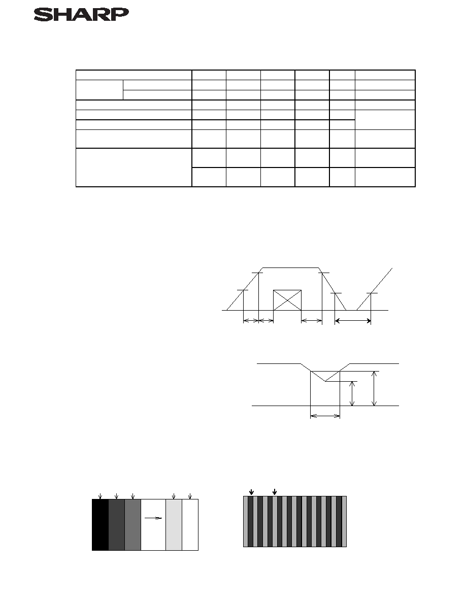
Note 6-2 Vcc = 3.3VV/Q = ""
Typical current situation: Timing; Typical64-gray-bar pattern.
Max current situation: Timing; TypicalVertical stripe pattern alternating
0 gray scale (GS0) with 42 gray scale (GS42) every 1 dot.
Typical current situation Max current situation
RGB
GS0
RGB
GS3
RGB
GS7
RGB
GS59
RGB
GS63
....
td
2.4V
3.0V
Vcc
GS0
GS42
t1
t2
t3
0.3V
3.0V
3.0V
Vcc
data
t4
0.3V
0.3V
LA1-05016-6
Note 6-3 CK,R0R5,G0G5,B0B5,Hsync,Vsync,ENAB,R/L,U/D,V/Q
Note 6-4 CK,R0R5,G0G5,B0B5,Hsync,Vsync,R/L,U/D
Note 6-5 ENABV/Q
6-2. Backlight driving section
The backlight system is an edge-lighting type with single CCFT (Cold Cathode Fluorescent Tube).
The characteristics of Lamp are shown in the following table.
Table 6-2
Parameter Symbol
Unit Remarks
lamp voltage
620
690 760 Vrms
5 mArms
lamp current
4.5 5.0 5.5
mArms
ordinary
state
lamp power
WL
-
3.5
-
W ratings
lamp frequency
30
-
60 kHz
kick-off Ta=+25
-
-
1350
voltage
Ta=-10
-
-
1470
Vrms
A shield is
connected to GND.
( Inverter HIU-288 [ Output condenser : 22pF ] TOSHIBA HARISON LIGHTING co. Ltd.)
Caution
Use the inverter providing symmetrical sine-wave in positive/negative polarity with no spike.
A shield(module's metal shield) should be connected to GND of inverter circuit.
7. Timing Characteristics of input signals
Timing diagrams of input signal are shown in Fig.7
7-1. Timing characteristics
Table 7-1
Parameter
Symbol
MIN
TYP
MAX
Unit
Remarks
Clock
-
25.18
28.33
MHz V/Q = H
frequency 1/Tc
-
6.3
7.0
V/Q = L
Duty
ratio
TH/T
40
50
60
%
Data Setup
time
Tds
5
-
-
ns
Hold
time
Tdh
10
-
-
ns
TH 30.0 31.8 -
s V/Q = H
770
800 900
clock
TH 50.0 63.6 -
s V/Q = L
Cycle
360
400 450
clock
Horizontal sync.
signal
Pulse width
THp
2
96
200
clock
Vertical sync.
Cycle
TV
515
525
560
line V/Q = H
signal
251
262
280
V/Q = L
Pulse
width
TVp
2
-
34 line
Horizontal display period
THd
320
320
320
clock
Hsync-Clock phase difference
THc
10
-
Tc-10
ns
Hsync-Vsync phase difference
TVh
0
-
TH-THp s
Vertical display start position
TVs
34
34
34
line V/Q = H
7
7
7
V/Q = L
Note) In case of lower frequency, the deterioration of display quality, flicker etc., may be occurred.
7-2. Horizontal display position
The horizontal display position is determined by the rising edge of ENAB signal.
Table 7-2
Parameter symbol
Min.
Typ.
Max.
Unit
Remark
Enable signal
Setup time
Tes
5
-
Tc-10
ns
Pulse
width
Tep
2
320
TH-10
clock
The 44 - TH-664 clock V/Q = H
Hsync-Enable signal phase
difference
2
TH-340
V/Q = L
Note) When ENAB is fixed "Low", the display starts from the following data as shown in Fig.7.
V/Q = "H" C104 (clock) V/Q = "L" C52 (clock)
LA1-05016-7
7-3. Vertical display position
The Vertical display start position (TVs) is fixed 34 line (V/Q =H) and 7 line (V/Q = L).
ENAB signal has no relation to the vertical display position.
7-4. Input Data Signals and Display Position on the screen
Display position of input data (H,V)
D1,DH1
D1,DH2
D1,DH3
D1,DH240
D2,DH1
D320,DH240
D320,DH1
D2,DH2
R
D3,DH1
G B
LA1-05016-8
Horizontal sync.
signal
Hsync
Clock signal
CK
DataR05
G05B05
Data Enable signal
ENAB
Vertical Sync
signal
Vsync
Horizontal sync
signal
Hsync
DataR05
G05B05
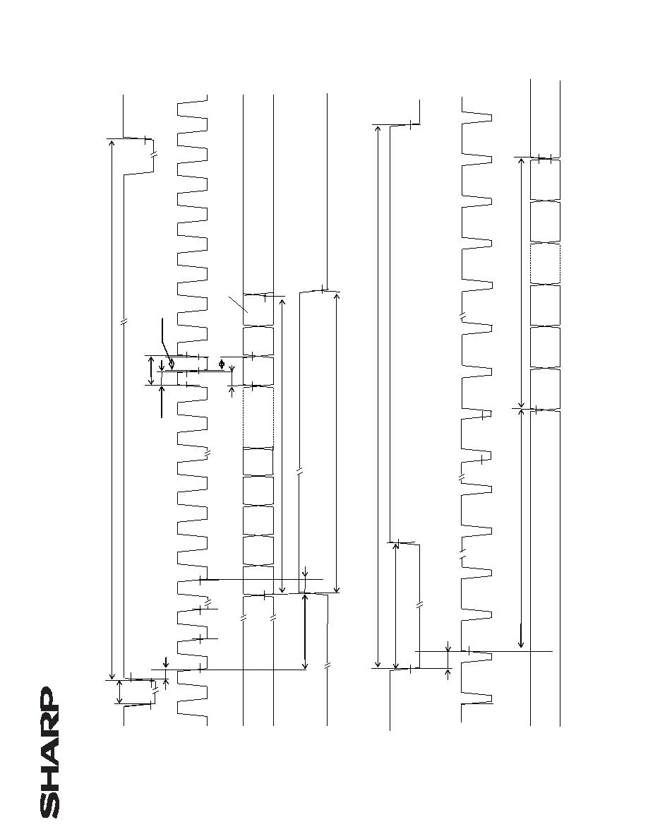
Fig 7. Input signal waveforms
0.3Vcc
0.7Vcc
TVp
TV
0.3Vcc
TVh
Vertical invalid data period
DH1 DH2 DH3
Vertical invalid
data
period
DH239 DH240
TVs
THp
0.7Vcc
0.3Vcc
Tch
Tcl
Tc
0.3Vcc
TH
THc
0.3Vcc
Horizintal invalid data period
Horizontal invalid data period
D2
D1
D3
D318 D319
Tds
Tdh
Tes
0.7Vcc
Tep
0.3Vcc
THd
The
C104(V/Q=H)
C52(V/Q=L)
(Number of clock)
C2
C1
Only when enable terminal is fixed "Low"
0.7Vcc
Line1 Line2
D4
D320
D5
0.3Vcc
Line34(V/Q=H)
Line7(V/Q=L)
(Number of Vertical count)
0.3Vcc 0.3Vcc 0.3Vcc
TVd
Number of Horizontal data
0.7Vcc
LA1-05016-9
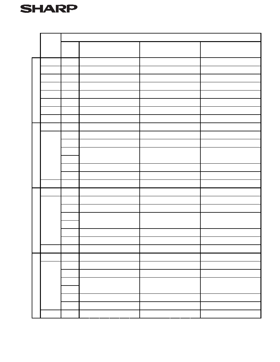
() Input Signals, Basic Display Color and Gray Scale of Each Color
Colors & Data signal
Gray scale Gray
Scale
R0 R1 R2 R3 R4 R5 G0 G1 G2 G3 G4 G5 B0 B1 B2 B3 B4 B5
Black
-
0 0 0 0 0 0 0 0 0 0 0 0 0 0 0 0 0 0
Blue
-
0 0 0 0 0 0 0 0 0 0 0 0 1 1 1 1 1 1
Green
-
0 0 0 0 0 0 1 1 1 1 1 1 0 0 0 0 0 0
Cyan
-
0 0 0 0 0 0 1 1 1 1 1 1 1 1 1 1 1 1
Red
-
1 1 1 1 1 1 0 0 0 0 0 0 0 0 0 0 0 0
Magenta
-
1 1 1 1 1 1 0 0 0 0 0 0 1 1 1 1 1 1
Yellow
-
1 1 1 1 1 1 1 1 1 1 1 1 0 0 0 0 0 0
Basic color
White
-
1 1 1 1 1 1 1 1 1 1 1 1 1 1 1 1 1 1
Black GS0 0 0 0 0 0 0 0 0 0 0 0 0 0 0 0 0 0 0
GS1 1 0 0 0 0 0 0 0 0 0 0 0 0 0 0 0 0 0
Darker GS2 0 1 0 0 0 0 0 0 0 0 0 0 0 0 0 0 0 0
Brighter GS61 1 0 1 1 1 1 0 0 0 0 0 0 0 0 0 0 0 0
GS62 0 1 1 1 1 1 0 0 0 0 0 0 0 0 0 0 0 0
Gra
y
Scale of red
Red GS63 1 1 1 1 1 1 0 0 0 0 0 0 0 0 0 0 0 0
Black GS0 0 0 0 0 0 0 0 0 0 0 0 0 0 0 0 0 0 0
GS1 0 0 0 0 0 0 1 0 0 0 0 0 0 0 0 0 0 0
Darker GS2 0 0 0 0 0 0 0 1 0 0 0 0 0 0 0 0 0 0
Brighter GS61 0 0 0 0 0 0 1 0 1 1 1 1 0 0 0 0 0 0
GS62 0 0 0 0 0 0 0 1 1 1 1 1 0 0 0 0 0 0
Gra
y
Scale of
g
reen
Green GS63 0 0 0 0 0 0 1 1 1 1 1 1 0 0 0 0 0 0
Black GS0 0 0 0 0 0 0 0 0 0 0 0 0 0 0 0 0 0 0
GS1 0 0 0 0 0 0 0 0 0 0 0 0 1 0 0 0 0 0
Darker GS2 0 0 0 0 0 0 0 0 0 0 0 0 0 1 0 0 0 0
Brighter GS61 0 0 0 0 0 0 0 0 0 0 0 0 1 0 1 1 1 1
GS62 0 0 0 0 0 0 0 0 0 0 0 0 0 1 1 1 1 1
Gra
y
Scale of bleu
Bleu GS63 0 0 0 0 0 0 0 0 0 0 0 0 1 1 1 1 1 1
0 :Low level voltage 1 :High level voltage
Each basic color can be displayed in 64 gray scales from 6 bit data signals. According to the
combination of total 18 bit data signals, the 262,144-color display can be achieved on the screen.
LA1-05016-10
9. Optical characteristics
Table 9-1 Ta=25VCC = 3.3V
Parameter Symbol
Condition
Min
Typ
Max
Unit
Remarks
21, 22
60 65 -
°
(degree) Note 9-1
Viewing angle range
11 CR5
60 65 -
°
(degree)
12
35 40 -
°
(degree)
Contrast ratio
CRmax
Optimal
viewing angle
250 350 -
Note 9-2
Response Rise
r
°
-
8 20
ms
Note 9-3
time Fall
d
-
21 40 ms
White chromaticity
x
0.263
0.313
0.363
y
IL=5mArms
0.279
0.329
0.379
Note 9-4
Luminance Y
350
500
-
cd/m
2
lamp life time +25
- continuation
40,000 50,000 -
hour
Note 9-5
Lamp test in the module is made with the following inverter:.
HIU-288 [ Output condenser : 22pF ] TOSHIBA HARISON LIGHTING co. Ltd.
The optical specifications are measured 30 minute after turing lamp on and in a dark room or
equivalent condition, according to the method shown in Fig.9-1 below.
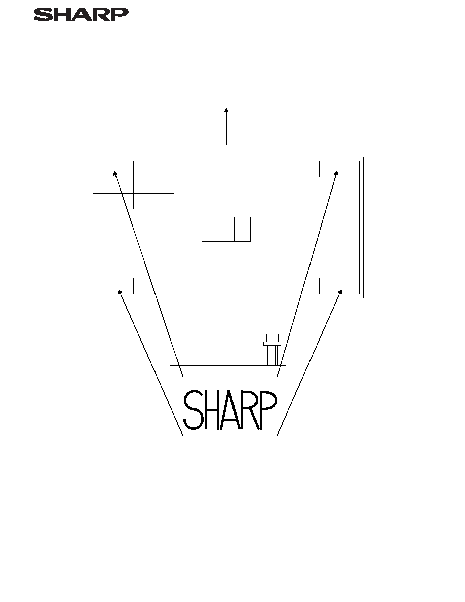
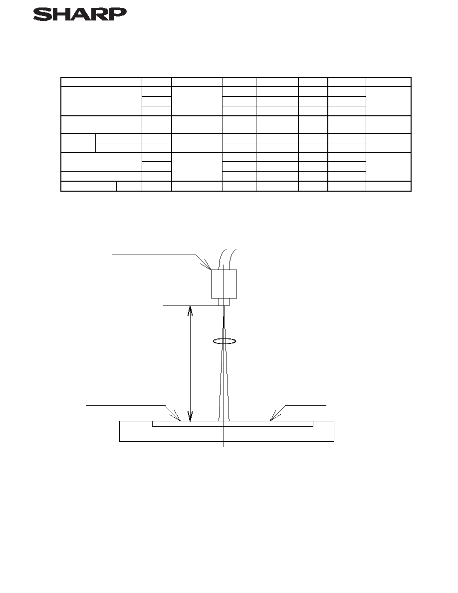
Fig.9-1 Optical characteristics measurement method
Photodetector (BM-5A : TOPCON)
Center of the screen
TFT-LCD Module
LCD panel
Field=2°
400
LA1-05016-11
Note 9-1 Viewing angle range is defined as follows.
12 o'clock
direction
6 o'clock direction
Normal line
21
22
11
12
The best viewing angle of this module is slightly leaned to 12 o'clock from normal line.
Where
11
max
, gray scale is reversed partially.
Where
11
max
, or in
12
direction, gray scale isn't reversed.
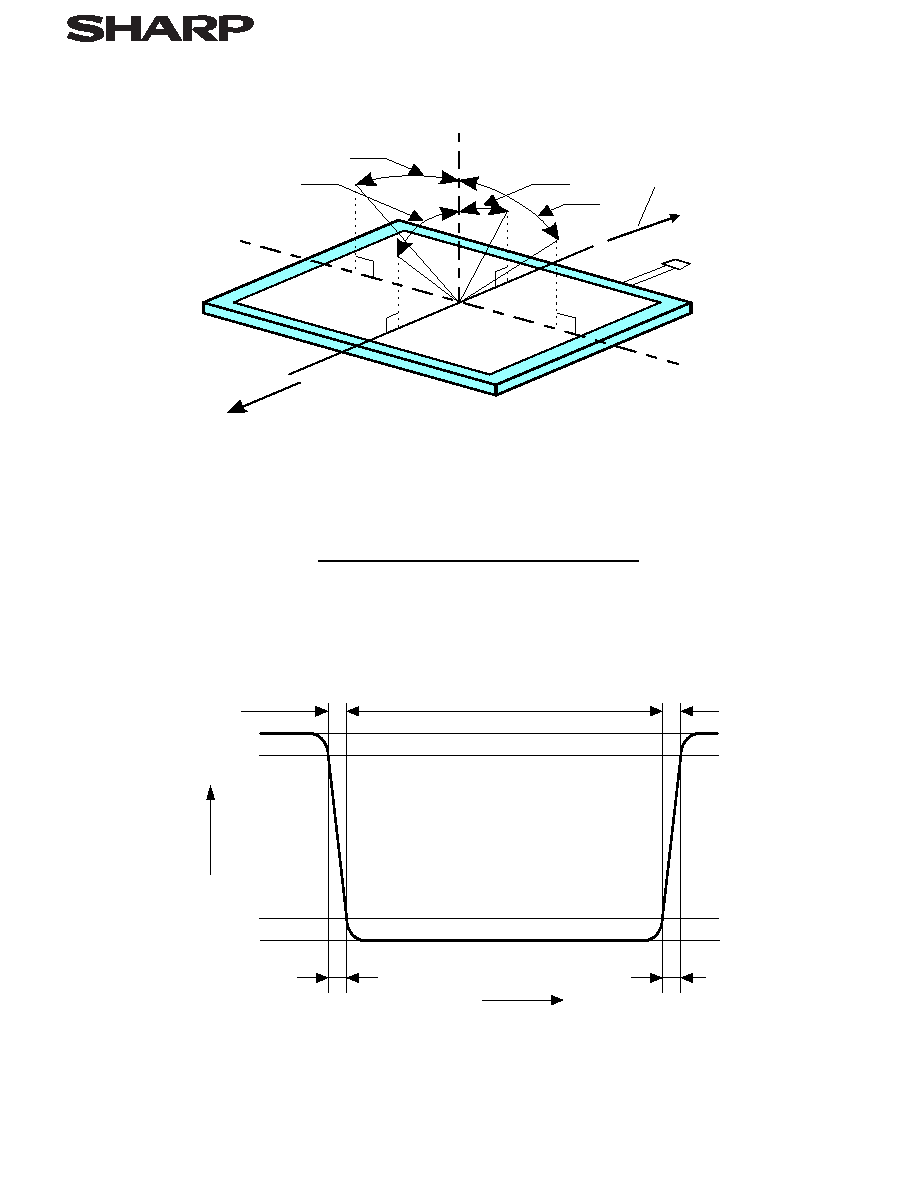
Note 9-2 Contrast ratio is defined as follows:
Luminance (brightness) with all pixels white
Contrast ratio(CR)=
Luminance (brightness) with all pixels black
Measurement point : Center of the active area
Note 9-3 Response time is obtained by measuring the transition time of photo detector
output, when input signals are applied so as to make the area "black" to and
from "white".
Black White
White
Time
P
h
o
t
o
d
e
t
e
c
t
e
r
o
u
t
p
u
t
(
R
e
l
a
t
i
v
e
v
a
l
u
e
)
Note 9-4 This parameter should be measured at the center of the screen and 30 minutes after turn-
on.
Inverter frequency: 49kHz
The characteristics are measured when the driver circuit is not powered.
Note 9-5 The data for lamp is for your reference, because lamp is consumable component.

LA1-05016-12
a)
Lamp life time is defined by either 1 or 2 below.
(Continuous turning on at Ta=25, IL=5mA rms)
When a brightness of lamp surface become 50% of the initial value under the
standard condition.
When a kick-off voltage in Ta=-10 exceeded maximum value(1470 Vrms)
at the output of inverter circuitry.
b)
In case of operating under lower temp. environment, the lamp exhaustion is accelerated
and the brightness becomes lower.
(Continuous operating for around 1 month under lower temp. condition may reduce the
brightness to half of the original brightness.)

LA1-05016-13
10. Handling instructions
10-1. Mounting of modules
The TFT-LCD module is designed to be mounted on equipment using the mounting
tabs in the four corners of the module at the rear side. On mounting the module, as the
nominal diameter 3.0mm tapping screw (fastening torque is 0.25 through
0.30 Nm) is recommended, be sure to fix the module on the same plane, taking care not
to wrap or twist the module. The depth of tapping screw embedded into LCD module must
be less than 5mm.
The pressing module, (ex. touching switch etc.) causes disordered image. So taking care
for pressure not to conduct directly to LCD module.
Please power off the module before you connect or disconnect input connector.
Connect the metallic shielding cases of the module and the ground pattern of the inverter
circuit firmly. If that connection is not perfect, there may be a possibility that the following
problems happen.
a) The noise from the backlight unit will increase.
b) The output from inverter circuit will be unstable.
c) In some cases, a part of module will heat up.
10-2. Precautions in mounting
Polarizer which is made of soft material and susceptible to flaw must be handled carefully.
Method of removing dust from polarizer.
Blow off dust with N2 blower for which static electricity preventive measure has
been taken.
Since the polarizer is easily damaged, wiping should be avoided. If the panel has stain
or finger grease, we recommend to use adhesive tape to softly remove them from the panel.
Inevitable, wipe off by cleaning cloth for a lens with carefully, breathing on it.
When metal part of the TFT-LCD module (shielding lid and rear case) is soiled, wipe it
with soft dry cloth. For stubborn dirties, wipe the part, breathing on it.
Wipe off water drop or finger grease immediately. Long contact with water may cause
discoloration or spots.
TFT-LCD module uses glass which breaks or cracks easily if dropped or bumped on hard surface.
handle with care.
Since CMOS LSIs are incorporated in this module, take care of electrostatic and earth human
body while handling.
10-3. Caution of product design
The notes and cautions below should be followed when product is designed with this module.
The LCD module should be protected against water salt-water by the waterproof cover.
Take enough shielding countermeasure not to interfere to peripheral electric device.
10-4. Others
Do not expose the module to direct sunlight or intensive ultraviolet rays for many hours;
liquid crystal is deteriorated by ultraviolet rays.
If stored at the temperature lower than rated temperature, the liquid crystal may freeze and
it may cause LCD panel damage. If storage temperature exceeds the specified rating, the
molecular orientation of the liquid crystal may change to that of a liquid, and they may not
revert to their original state. Store the module in normal room temperature.
The voltage of beginning electric discharge may over the normal voltage because of leakage
current from approach conductor by to draw lump lead line around.
If LCD panel breaks, there may be a possibility that the liquid crystal escapes from the panel.
If the liquid crystal drip into the eyes or mouth washes it out immediately.
The caution to other ordinal electronic component should be followed also.
LA1-05016-14
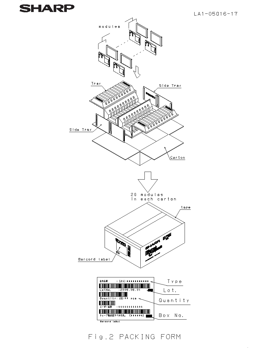
11. Shipping requirements
a) Number of layers of cartons in pile : 12 layers max.
b) Maximum number of product contained: 20 units per 1 carton.
c) Carton size : 442mm(W)×390mm(H)×170mm(D)
d) Total mass ( for 20 units ) : Approximately 5.5
e) Carton stock environment :
Temperature 0 to 40
Humidity 60%RH or less
Atmosphere Harmful gases such as acid and alkali which corrode electric
components and wires must not be detected.
Storage period Approximately 3 months
Opening of package To prevent TFT-LCD module from being damaged by electrostatic,
adjust the humidity to 50%RH or higher and provide
an appropriate measure for electrostatic earthing before
opening the package.
12. Others
a) Adjusting volumes have been set optimally before shipment. Therefore, do not change any
adjusted values. If adjusted values are changed, the specifications described here may not be
satisfied.
b) Disassembled the module, it may cause malfunction.
c) Be careful since image retention may occur when a fixed pattern is displayed for a long time.
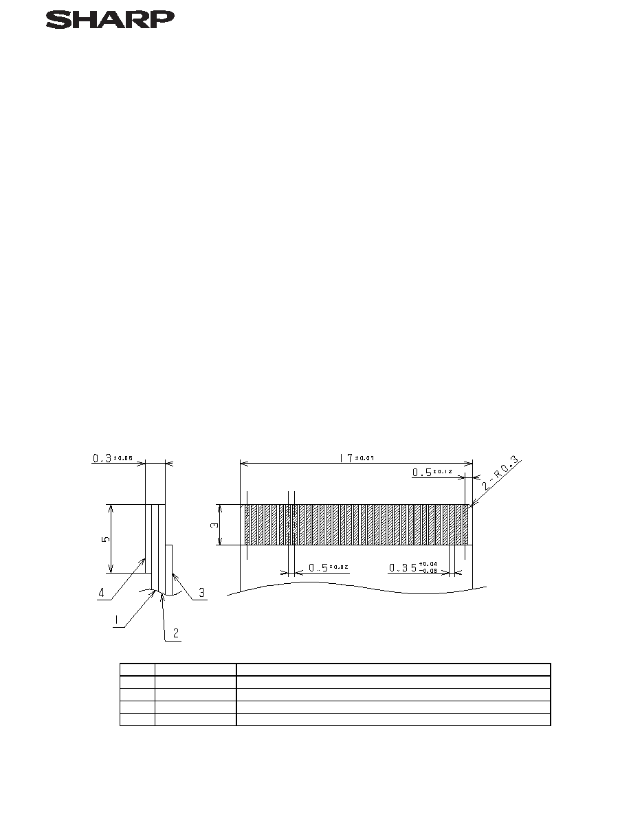
d) Input/Output connector for TFT-LCD panel driving part
Used connector : FH12-33S-0.5SH(55) (HIROSE ELECTRIC C0.,LTD.)
1) Fit FPC : Refer to the following figure
2) Keeping power of terminal : 0.9N/pin or more
[ Every terminal is pulled out 25±3mm/minute ]
3) Endurance of insert/pull out : Less than double of the initial resistance value
[ The electrical resistance value of the contact changed by the repeated insertion/pulling
out by 20 times to and from the matching FPC ]
No. Parameter
Material
1
Base material
Polyimide or the equivalent [ 25um thickness ]
2
Copper leaf
Copper leaf [ 35um thickness ] gold leaf[ 2um or more thickness ]
3
Coverlay
Polyimide or the equivalent
4
Reinforced sheet Polyester, polyimide or the equivalent [ 188um thickness ]
Fit FPC for Input/Output connector : 0.5mm pitch
LA1-05016-15
13. Reliability Test Conditions for TFT-LCD Module
Table 13-1
No.
Test items
Test conditions
High temperature
storage test
Leaves the module at Ta = +80 for 240h Note 1
Low temperature
storage test
Leaves the module at Ta=-30 for 240h Note 1
High temperature
and high humidity
operating test
Operates the module at Tp= +40, 95%RH for 240h
(No condensation) Note 1
High temperature
operating test
Operates the module at Tp= +70 for 240h Note 1
Low temperature
operating test
Operates the module at Ta=-10 for 240h Note 1
(The lifetime of a CCFT is not included)
Strength against
ESD
±
200V200pF(0) 1 time for each terminals
Shock test
(non-operating)
490m/s26ms, ±X±Y±Z 3 times for each direction
JIS C0041, A-7 Condition C
Vibration test
(non-operating)
Frequency557Hz, Stroke0.15mm
Frequency58500Hz, Acceleration9.8m/s
2
Sweep cycle11 minutes
X,Y,Z 1 hours for each directions ( total 3 hours ) Note 2
JIS D1601
Thermal shock test Ta=-30+80 , 200 cycles
(0.5h) (0.5h)
Result evaluation criteria
Under the display quality test conditions with normal operation state, these shall be
no change which may affect practical display function.
Note 1 Ta= Ambient temperature, Tp= Panel surface temperature
Note 2 X,Y,Z directions are shown as follows:

SPECIFICATIONS ARE SUBJECT TO CHANGE WITHOUT NOTICE.
Suggested applications (if any) are for standard use; See Important Restrictions for limitations on special applications. See Limited
Warranty for SHARP's product warranty. The Limited Warranty is in lieu, and exclusive of, all other warranties, express or implied.
ALL EXPRESS AND IMPLIED WARRANTIES, INCLUDING THE WARRANTIES OF MERCHANTABILITY, FITNESS FOR USE AND
FITNESS FOR A PARTICULAR PURPOSE, ARE SPECIFICALLY EXCLUDED. In no event will SHARP be liable, or in any way responsible,
for any incidental or consequential economic or property damage.
NORTH AMERICA
EUROPE
JAPAN
SHARP Microelectronics of the Americas
5700 NW Pacific Rim Blvd.
Camas, WA 98607, U.S.A.
Phone: (1) 360-834-2500
Fax: (1) 360-834-8903
Fast Info: (1) 800-833-9437
www.sharpsma.com
SHARP Microelectronics Europe
Division of Sharp Electronics (Europe) GmbH
Sonninstrasse 3
20097 Hamburg, Germany
Phone: (49) 40-2376-2286
Fax: (49) 40-2376-2232
www.sharpsme.com
SHARP Corporation
Electronic Components & Devices
22-22 Nagaike-cho, Abeno-Ku
Osaka 545-8522, Japan
Phone: (81) 6-6621-1221
Fax: (81) 6117-725300/6117-725301
www.sharp-world.com
TAIWAN
SINGAPORE
KOREA
SHARP Electronic Components
(Taiwan) Corporation
8F-A, No. 16, Sec. 4, Nanking E. Rd.
Taipei, Taiwan, Republic of China
Phone: (886) 2-2577-7341
Fax: (886) 2-2577-7326/2-2577-7328
SHARP Electronics (Singapore) PTE., Ltd.
438A, Alexandra Road, #05-01/02
Alexandra Technopark,
Singapore 119967
Phone: (65) 271-3566
Fax: (65) 271-3855
SHARP Electronic Components
(Korea) Corporation
RM 501 Geosung B/D, 541
Dohwa-dong, Mapo-ku
Seoul 121-701, Korea
Phone: (82) 2-711-5813 ~ 8
Fax: (82) 2-711-5819
CHINA
HONG KONG
SHARP Microelectronics of China
(Shanghai) Co., Ltd.
28 Xin Jin Qiao Road King Tower 16F
Pudong Shanghai, 201206 P.R. China
Phone: (86) 21-5854-7710/21-5834-6056
Fax: (86) 21-5854-4340/21-5834-6057
Head Office:
No. 360, Bashen Road,
Xin Development Bldg. 22
Waigaoqiao Free Trade Zone Shanghai
200131 P.R. China
Email: smc@china.global.sharp.co.jp
SHARP-ROXY (Hong Kong) Ltd.
3rd Business Division,
17/F, Admiralty Centre, Tower 1
18 Harcourt Road, Hong Kong
Phone: (852) 28229311
Fax: (852) 28660779
www.sharp.com.hk
Shenzhen Representative Office:
Room 13B1, Tower C,
Electronics Science & Technology Building
Shen Nan Zhong Road
Shenzhen, P.R. China
Phone: (86) 755-3273731
Fax: (86) 755-3273735