IS1685
IS1685
1. OPIC light detector with built-in RF amplifier
(Integrates 6-division PIN photodiode and Amp. IC onto a
single chip)
2. High speed response
(Response frequency : MIN. 57.4MHz)
3. Can read various discs such as DVD, DVD-ROM,
DVD-R, CD-ROM, CD-R
4. High sensitivity
5. Compact and thin package
(Package dimensions : 5.0x4.0x1.5mm)
6. Possible to supply custom-made detecting patterns
7. Pair use with SHARP's laser diode is recommended.
Laser diode : 650nm band
GH06510A2A/B
OPIC Light Detector for
DVD Player (X6 Speed)
s
Features
1. DVD drives
2. CD-ROM drives
s
Applications
s
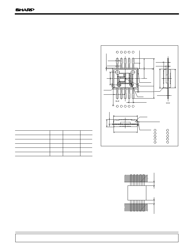
Outline Dimensions
(Unit : mm)
s
Absolute Maximum Ratings
*1 Applies to V
A
to V
F
terminal.
*2 For MAX. 3s at the position of 1.0mm from the bottom face of resin package.
Parameter
Symbol
Rating
Unit
Supply voltage
V
CC
*1
Output voltage
V
O
V
V
Operating temperature
T
opr
-
30 to
+
80
�
C
Storage temperature
T
stg
-
40 to
+
100
6.0
V
CC
�
C
*2
Soldering temperature
T
sol
+
260
�
C
(Ta
=
25
�
C)
2.5
�
0.2
8.4
�
0.3
2.0
�
0.2
(2.2)
4.9
�
0.2
1.5
�
0.1
P0.8
�
0.1
Edge
Gate burr
Detector center
(R0.3)
(R0.3)
(1.3)
(1.3)
Reference
face
(0.85)
(0.37)
Reference
face
(0.97)
(1.2)
Y
Y'
Thick burr 1.2
MAX.
Thick burr 0.2
MAX.
0.4
+
0.2
-
0.1
0.35
+
0.2
-
0.1
4.0
+
0.05
-
0.1
5.0
+
0.05
-
0.1
3.9
�
0.2
0.15
+
0.3
-
0
10
9
8
7
6
1
2
3
4
5
1
2
3
4
5
6
7
8
9
10
Thin burr 0.4
MAX.
10-
10-
V
D
V
A
V
RF
V
B
V
C
V
E
GND
V
S
V
CC
V
F
g
( ) : Reference dimensions
X
X'
(1.6)
(1.1)
(1.1)
(1.3)
Rest of gate
(
0.8)
"OPIC"(Optical IC) is a trademark of the SHARP Corporation.
An OPIC consists of a light-detecting element and signal-
processing circuit integrated onto a signal chip.
Notice
In the absence of confirmation by device specification sheets, SHARP takes no responsibility for any defects that may occur in equipment using any SHARP
devices shown in catalogs, data books, etc. Contact SHARP in order to obtain the latest device specification sheets before using any SHARP device.
Internet
Internet address for Electronic Components Group http://www.sharp.co.jp/ecg/
1.0mm
1.0mm
Soldering area
Soldering area
IS1685
s
Electro-optical Characteristics 1
s
Electro-optical Characteristics 2
Parameter
Symbol
MIN.
TYP.
MAX.
Unit
Application
Supply current
I
CC
20
V
od1
V
od2
V
od3
Conditions
-
A
-
B
C
-
D
(A
+
C)
-
(B
+
D)
E
-
F
Specified by voltage difference from Vs
Specified by voltage difference from Vs
GND reference
+
25
+
15
1.55
Vcc
V
A
to V
D
V
A
to V
D
V
A
to V
D
V
E
, V
F
V
E
, V
F
V
RF
Output off-set voltage 1
Output off-set voltage 3
Output off-set voltage 2
8.8
-
15
-
25
-
20
-
20
-
20
1.25
14.8
0
0
0
0
1.4
mA
mV
V
mV
V
od
A
+
B
+
C
+
D
V
A
, V
B
V
C
, V
D
Extremes of off-set voltage
-
100
-
15
+
20
+
20
+
20
+
100
+
15
0
0
0
mV
(Ta
=
25
�
C, Vcc
=
5V, V
S
=
2.1V, R
L
=
10k
[V
RF
:
Open], C
L
=
5
pF
)
-
f
=
23.1MHz, BW
=
30kHz
f
=
23.1MHz, BW
=
30kHz
Output noise level 1
Output noise level 2
V
RF
V
A
to V
D
-
-
70
-
65
V
n1
V
n2
-
81
-
76
dBm
dBm
V
RF
V
RF
V
RF
V
A
to V
D
V
A
to V
D
V
E
, V
F
V
E
, V
F
Parameter
Symbol
MIN.
TYP.
MAX.
Unit
Application
Sensitivity 1
R
p1
-
-
-
-
-
-
-
-
-
-
-
-
-
-
-
25.4
R
p2
R
p3
R
p1
R
p2
/R
p1
R
p3
/R
p1
V
OH1
V
OH2
Conditions
-
-
-
-
-
-
f
=
1 to 23.1MHz
f
=
1 to 23.1MHz, Average of V
A
to V
D
-
3dB
-
3dB
-
3dB
-
3dB Applied to the center of the divided portion
47.4
32.4
10
%
V
V
1.17
36
45
1
14.7
25.4
17.4
20.0
36.4
24.9
1.81
1.24
1.30
MHz
V
RF
57.4
77
-
60
70
5
mV/
�
W
mV/
�
W
mV/
�
W
(Ta
=
25
�
C, Vcc
=
5V, V
S
=
2.1V, R
L
=
10k
[V
RF
:
Open], C
L
=
5pF)
*3*4
Sensitivity 2
Sensitivity ratio 1
Sensitivity ratio 2
*3*4
Sensitivity 3
*3*4
Extreme of sensitivity 1
*5
High level output voltage 1
High level output voltage 2
*4
*4
V
A
to V
D
V
RF
V
A
to V
D
-
-
-
f
c1
f
c2
f
c3
f
c4
tgd1
tgd2
-
-
3.8
3.8
2.5
2.5
5.5
5.5
ns
ns
MHz
MHz
MHz
Response frequency 1
*4*6*7
Group delay deviation 1
*4, *7
Group delay deviation 2
*4, *7
Response frequency 2
*4*6*7
Response frequency 3
*4*6*7
Response frequency 4
*4*6*8
Input light source wavelength
p
=
650nm
s
Recommended Operating Conditions
Parameter
MIN.
TYP.
MAX.
Unit
Supply voltage 1
Supply voltage 2
5.25
Symbol
V
cc
V
S
V
V
5.0
2.1
2.2
4.75
2.0
(Ta
=
25
�
C)
IS1685
s
Electro-optical Characteristics 3
*3 5
�
W,
30
�
m of DC light is applied to the center of each photodiode.
Under that condition, sensitivity R
p
is shown by following formula.
R
p
=
(V
p
-
V
od
)5
�
W
*4 Light source : laser diode of
=
650nm or 780nm.
*5 Extreme of sensitivity is shown by following formula.
2 x (R
p1
max.
-
R
p1
min.) / (R
p1
max.
+
R
p1
min.) x 100
2 x (R
p2
max.
-
R
p2
min.) / (R
p2
max.
+
R
p2
min.) x 100
2 x (R
p4
max.
-
R
p4
min.) / (R
p4
max.
+
R
p4
min.) x 100
2 x (R
p5
max.
-
R
p5
min.) / (R
p5
max.
+
R
p5
min.) x 100
*6 Frequency sensitivity is
-
3dB. (reference sensitivity : value at f
=
1MHz)
*7 Refer to Fig.1
*8 Refer to Fig.1
*9 For Frequency Charactoristics refer to Fig.2
*10 As the temperature characteristics of the peaking rate A, the peaking rate at Ta=65�C against the peaking rate at Ta=25�C shall be satisfied with the following.
(Application terminal : V
A
to V
D
, V
RF
)
V
RF
V
RF
V
RF
V
A
to V
D
V
A
to V
D
V
E
, V
F
V
E
, V
F
Parameter
Symbol
MIN.
TYP.
MAX.
Unit
Application
Sensitivity 4
R
p4
-
-
-
-
-
-
-
-
-
-
-
-
-
-
-
31.2
R
p5
R
p6
R
p2
R
p5
/R
p4
R
p6
/R
p4
V
OH3
V
OH4
Conditions
-
-
-
-
-
-
f
=
1 to 23.1MHz
f
=
1 to 23.1MHz, Average of V
A
to V
D
-
3dB
-
3dB
-
3dB
58.1
39.7
10
%
V
V
1.17
34
43
1
18.0
31.2
21.3
24.6
44.7
30.5
1.81
1.24
1.30
57
68
5
mV/
�
W
mV/
�
W
mV/
�
W
(Ta
=
25
�
C, Vcc
=
5V, V
S
=
2.1V, R
L
=
10k
[V
RF
:
Open], C
L
=
5pF)
*3*4
Sensitivity 5
Sensitivity ratio 3
Sensitivity ratio 4
*3 *4
Sensitivity 6
*3 *4
Extreme of sensitivity 2
*5
High level output voltage 3
High level output voltage 4
*4
*4
V
A
to V
D
V
RF
V
RF
V
A
to V
D
-
-
-
f
c5
f
c6
f
c7
t
gd3
t
gd4
-
-
3.8
3.8
2.5
2.5
5.5
5.5
ns
ns
MHz
MHz
MHz
Response frequency 5
*4*6*7
Group delay deviation 3
*4, *7
Group delay deviation 4
MAX. 2.5dB
780nm
*4, *7
Response frequency 6
*4*6*7
Response frequency 7
*4*6*7
-
-
3dB Applied to the center of the divided portion
50
68
f
c8
MHz
Response frequency 8
*4*6*8
Input light source wavelength
p
=
780nm
MAX. 3.5dB
650nm
Fig.1 Response Frequency
Application : Response frequency except fc4 with
=
650nm, peaking rate, bottom rate, change rate,
group delay deviation
Response frequency except fc8 with
=
780nm peaking rate, bottom rate, change rate,
group delay deviation
*
7 In addition to 10
�
W,
30
�
m DC light, 4
�
Wp-p AC light is applied to the center of each photodiode. BW
=
10kHz
*
8 In addition to 10
�
W,
30mm DC light, 4
�
Wp-p of AC light is applied to the center of the divided
portion of photodiode A, B, C and D. BW
=
10kHz
D
Application : fc4 with
=
650nm and fc8 with
=
780nm
C
A
B
D
C
A
B
30
�
m
Laser light
30
�
m
Laser light
IS1685
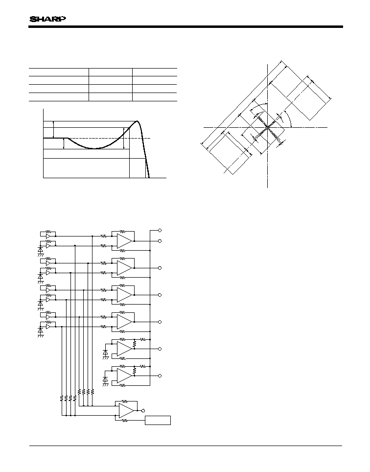
Fig.4 Block Diagram
-
+
V
S
V
A
V
B
V
C
V
D
V
E
V
F
V
RF
-
+
-
+
-
+
-
+
-
+
-
+
A
B
C
D
E
F
Bias circuit
Fig.2 Frequency Characteristics
Fig.3 Detecting Pattern of Photodiode
X�
X
Y�
Y
A
E
F
B
C
D
49
8
10
0
10
0
10
5
10
9
12
0
32
10
9
32
10
5
88
46
�
4
6
�
6
�
6
�
5
5
(Unit :
�
m)
(Reference)
A
B
1MHz
-
3dB
23.1MHz
fc
Frequency
The following 3 points shall be satisfied as frequency characteristics.
(Application : fc1, fc2, fc5, fc6)
(Ta
=
25
�
C, V
CC
=
5V, V
S
=
2.1V, R
L
=
10k
[V
RF
: Open], C
L
=
5pF)
(Reference frequency 1MHz)
S
e
n
s
i
t
i
v
i
t
y
(
d
B
)
C
780nm
Peaking rate A
MAX. 2.5dB
Bottom rate B
MAX. 1.0dB
Change rate C
MAX. 3.0dB
650nm
MAX. 3.5dB
MAX. 1.0dB
MAX. 4.0dB
IS1685
Fig.7 Output Offset Voltage 2 vs. Ambient
Temperature (V
E
, V
F
)
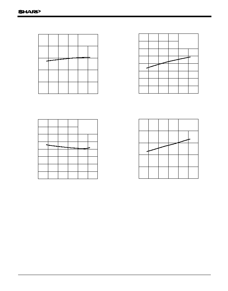
Fig.5 Supply Current vs. Ambient
Temperature
Fig.6 Output Offset Voltage 1 vs. Ambient
Temperature (V
A
to V
D
)
Fig.8 Output Offset Voltage 3 vs. Ambient
Temperature (V
RF
)
0
25
20
15
10
5
-
50
-
25
0
25
50
75
100
S
u
p
p
l
y
c
u
r
r
e
n
t
I
C
C
(
m
A
)
Ambient temperature T
a
(
�
C)
V
CC
=
5V
V
S
=
2.1V
O
u
t
p
u
t
o
f
f
s
e
t
v
o
l
t
a
g
e
1
V
o
d
1
(
m
V
)
Ambient temperature T
a
(
�
C)
-
20
20
15
10
5
0
-
5
-
10
-
15
-
50
-
25
0
25
50
75
100
V
CC
=
5V
V
S
=
2.1V
R
L
=
10k
C
L
=
5pF
O
u
t
p
u
t
o
f
f
s
e
t
v
o
l
t
a
g
e
2
V
o
d
2
(
m
V
)
Ambient temperature T
a
(
�
C)
-
20
20
15
10
5
0
-
5
-
10
-
15
-
50
-
25
0
25
50
75
100
V
CC
=
5V
V
S
=
2.1V
R
L
=
10k
C
L
=
5pF
O
u
t
p
u
t
o
f
f
s
e
t
v
o
l
t
a
g
e
3
V
o
d
3
(
V
)
Ambient temperature T
a
(
�
C)
0.0
2.5
2.0
1.5
1.0
0.5
-
50
-
25
0
25
50
75
100
V
CC
=
5V
V
S
=
2.1V
C
L
=
5pF
IS1685
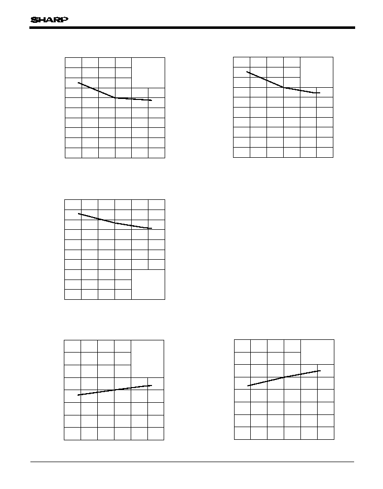
Fig.11 Response Frequency 4 vs. Ambient Temperature
(V
RF
: Applied to The Center of The Divided Portion)
Fig.10 Response Frequency 2 vs. Ambient
Temperature (V
RF
)
Fig.13 Sensitivity 3 vs. Ambient Temperature
(V
RF
)
Fig.9 Response Frequency 1 vs. Ambient
Temperature (V
A
to V
D
)
R
e
s
p
o
n
s
e
f
r
e
q
u
e
n
c
y
1
f
c
1
(
M
H
z
)
Ambient temperature T
a
(
�
C)
0
100
90
80
70
60
50
40
30
20
10
-
50
-
25
0
25
50
75
100
=
650nm
V
CC
=
5V
V
S
=
2.1V
R
L
=
10k
C
L
=
5pF
R
e
s
p
o
n
s
e
f
r
e
q
u
e
n
c
y
2
f
c
2
(
M
H
z
)
Ambient temperature T
a
(
�
C)
0
100
90
80
70
60
50
40
30
20
10
-
50
-
25
0
25
50
75
100
=
650nm
V
CC
=
5V
V
S
=
2.1V
C
L
=
5pF
R
e
s
p
o
n
s
e
f
r
e
q
u
e
n
c
y
4
f
c
4
(
M
H
z
)
Ambient temperature T
a
(
�
C)
0
100
90
80
70
60
50
40
30
20
10
-
50
-
25
0
25
50
75
100
=
650nm
V
CC
=
5V
V
S
=
2.1V
C
L
=
5pF
Fig.12 Sensitivity 1 vs. Ambient Temperature
(V
A
to V
D
)
S
e
n
s
i
t
i
v
i
t
y
1
R
p
1
(
m
V
/
�
W
)
Ambient temperature T
a
(
�
C)
0
40
35
30
25
20
15
10
5
-
50
-
25
0
25
50
75
100
=
650nm
V
CC
=
5V
V
S
=
2.1V
R
L
=
10k
C
L
=
5pF
S
e
n
s
i
t
i
v
i
t
y
3
R
p
3
(
m
V
/
�
W
)
Ambient temperature T
a
(
�
C)
0
40
35
30
25
20
15
10
5
-
50
-
25
0
25
50
75
100
=
650nm
V
CC
=
5V
V
S
=
2.1V
C
L
=
5pF

115
Application Circuits
NOTICE
qThe circuit application examples in this publication are provided to explain representative applications of
SHARP devices and are not intended to guarantee any circuit design or license any intellectual property
rights. SHARP takes no responsibility for any problems related to any intellectual property right of a
third party resulting from the use of SHARP's devices.
qContact SHARP in order to obtain the latest device specification sheets before using any SHARP device.
SHARP reserves the right to make changes in the specifications, characteristics, data, materials,
structure, and other contents described herein at any time without notice in order to improve design or
reliability. Manufacturing locations are also subject to change without notice.
qObserve the following points when using any devices in this publication. SHARP takes no responsibility
for damage caused by improper use of the devices which does not meet the conditions and absolute
maximum ratings to be used specified in the relevant specification sheet nor meet the following
conditions:
(i) The devices in this publication are designed for use in general electronic equipment designs such as:
--- Personal computers
--- Office automation equipment
--- Telecommunication equipment [terminal]
--- Test and measurement equipment
--- Industrial control
--- Audio visual equipment
--- Consumer electronics
(ii)Measures such as fail-safe function and redundant design should be taken to ensure reliability and
safety when SHARP devices are used for or in connection with equipment that requires higher
reliability such as:
--- Transportation control and safety equipment (i.e., aircraft, trains, automobiles, etc.)
--- Traffic signals
--- Gas leakage sensor breakers
--- Alarm equipment
--- Various safety devices, etc.
(iii)SHARP devices shall not be used for or in connection with equipment that requires an extremely
high level of reliability and safety such as:
--- Space applications
--- Telecommunication equipment [trunk lines]
--- Nuclear power control equipment
--- Medical and other life support equipment (e.g., scuba).
qContact a SHARP representative in advance when intending to use SHARP devices for any "specific"
applications other than those recommended by SHARP or when it is unclear which category mentioned
above controls the intended use.
qIf the SHARP devices listed in this publication fall within the scope of strategic products described in the
Foreign Exchange and Foreign Trade Control Law of Japan, it is necessary to obtain approval to export
such SHARP devices.
qThis publication is the proprietary product of SHARP and is copyrighted, with all rights reserved. Under
the copyright laws, no part of this publication may be reproduced or transmitted in any form or by any
means, electronic or mechanical, for any purpose, in whole or in part, without the express written
permission of SHARP. Express written permission is also required before any use of this publication
may be made by a third party.
qContact and consult with a SHARP representative if there are any questions about the contents of this
publication.