1
www.semtech.com
RClamp0504P
RailClamp
Low Capacitance TVS Array
PROTECTION PRODUCTS - RailClamp
Description
Features
Circuit Diagram
PIN Configuration
Revision 02/14/2005
RailClamps
are low capacitance TVS arrays designed
to protect high speed data interfaces. This series has
been specifically designed to protect sensitive compo-
nents which are connected to data and transmission
lines from overvoltage caused by ESD (electrostatic
discharge), CDE (Cable Discharge Events), and EFT
(electrical fast transients).
The unique design incorporates surge rated, low
capacitance steering diodes and a TVS diode in a
single package. During transient conditions, the
steering diodes direct the transient current to ground.
The internal TVS diode clamps the transient voltage to
a safe level. The low capacitance array configuration
allows the user to protect up to four high-speed data
lines.
The RClamp0504P is in a 6-pin, RoHS compliant,
SLP1616P6 package. It measures 1.6 x 1.6 x
0.60mm. The leads are spaced at a pitch of 0.5mm
and are finished with lead-free NiPd. They may be
used to meet the ESD immunity requirements of IEC
61000-4-2, Level 4 (15kV air, 8kV contact discharge).
The combination of small size, low capacitance, and
high ESD surge capability makes them ideal for use in
portable applications such as cellular phones, next
generation color LCD displays, USB, and multi media
card interfaces.
Applications
Mechanical Characteristics
USB 2.0 and USB OTG
Multi Media Card (MMC) Interfaces
SD Card Interfaces
MDDI Ports
SIM Ports
Key Pads
Gigabit Ethernet
Transient protection for high-speed data lines to
IEC 61000-4-2 (ESD) ±15kV (air), ±8kV (contact)
IEC 61000-4-4 (EFT) 40A (5/50ns)
Array of surge rated diodes with internal TVS Diode
Small package (1.6 x 1.6mm) saves board space
Protects up to four I/O lines & power line
Low capacitance (<3pF) for high-speed interfaces
No insertion loss to 2.0GHz
2.0GHz
2.0GHz
2.0GHz
2.0GHz
Low leakage current and clamping voltage
Low operating voltage: 5.0V
Solid-state silicon-avalanche technology
SLP1616P6 6L package
RoHS Compliant
Nominal Dimensions: 1.6 x 1.6 x 0.60 mm
Lead Finish: NiPd
Molding compound flammability rating: UL 94V-0
Marking : 0504P
Packaging : Tape and Reel per EIA 481
SLP1616P6 (Bottom View)
5
1
3
4
6
GND
0.6
1.6
1.6
1
0.5
6
Nominal Dimensions in mm

2
2005 Semtech Corp.
www.semtech.com
PROTECTION PRODUCTS
RClamp0504P
Absolute Maximum Rating
Electrical Characteristics (T=25
o
C)
r
e
t
e
m
a
r
a
P
l
o
b
m
y
S
s
n
o
i
t
i
d
n
o
C
m
u
m
i
n
i
M
l
a
c
i
p
y
T
m
u
m
i
x
a
M
s
t
i
n
U
e
g
a
tl
o
V
f
f
O
-
d
n
a
t
S
e
s
r
e
v
e
R
V
M
W
R
D
N
G
o
t
5
n
i
P
5
V
e
g
a
tl
o
V
n
w
o
d
k
a
e
r
B
e
s
r
e
v
e
R
V
R
B
I
t
A
m
1
=
D
N
G
o
t
5
n
i
P
6
V
t
n
e
r
r
u
C
e
g
a
k
a
e
L
e
s
r
e
v
e
R
I
R
V
M
W
R
C
°
5
2
=
T
,
V
5
=
D
N
G
o
t
5
n
i
P
3
A
µ
e
g
a
tl
o
V
g
n
i
p
m
a
l
C
V
C
I
P
P
s
µ
0
2
/
8
=
p
t
,
A
1
=
D
N
G
o
t
n
i
p
O
/
I
y
n
A
5
1
V
e
g
a
tl
o
V
g
n
i
p
m
a
l
C
V
C
I
P
P
s
µ
0
2
/
8
=
p
t
,
A
6
=
D
N
G
o
t
n
i
p
O
/
I
y
n
A
5
2
V
e
g
a
tl
o
V
g
n
i
p
m
a
l
C
V
C
I
P
P
s
µ
0
2
/
8
=
p
t
,
A
6
=
D
N
G
o
t
5
n
i
P
8
1
V
e
c
n
a
ti
c
a
p
a
C
n
o
it
c
n
u
J
C
j
V
R
z
H
M
1
=
f
,
V
0
=
D
N
G
o
t
n
i
p
O
/
I
y
n
A
9
.
1
3
F
p
V
R
z
H
M
1
=
f
,
V
0
=
s
n
i
p
O
/
I
n
e
e
w
t
e
B
0
8
.
0
1
F
p
g
n
i
t
a
R
l
o
b
m
y
S
e
u
l
a
V
s
t
i
n
U
)
s
µ
0
2
/
8
=
p
t
(
r
e
w
o
P
e
s
l
u
P
k
a
e
P
P
k
p
0
5
1
s
t
t
a
W
)
s
µ
0
2
/
8
=
p
t
(
t
n
e
r
r
u
C
e
s
l
u
P
k
a
e
P
I
P
P
6
A
)
r
i
A
(
2
-
4
-
0
0
0
1
6
C
E
I
r
e
p
D
S
E
)
t
c
a
t
n
o
C
(
2
-
4
-
0
0
0
1
6
C
E
I
r
e
p
D
S
E
V
D
S
E
5
1
8
V
k
e
r
u
t
a
r
e
p
m
e
T
g
n
it
a
r
e
p
O
T
J
5
2
1
+
o
t
5
5
-
C
°
e
r
u
t
a
r
e
p
m
e
T
e
g
a
r
o
t
S
T
G
T
S
0
5
1
+
o
t
5
5
-
C
°
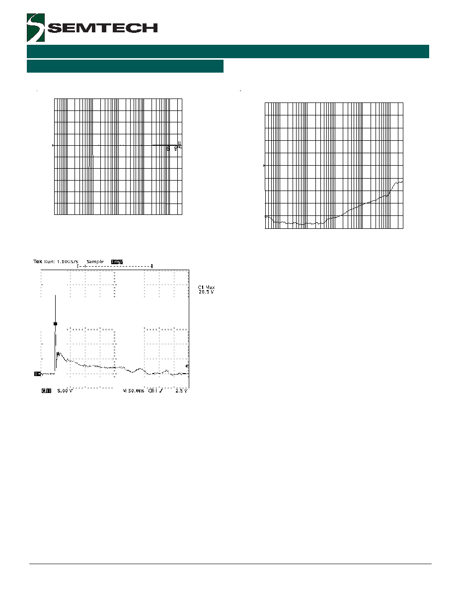
Note 1: I/O pins are pin 1, 3, 4, and 6
3
2005 Semtech Corp.
www.semtech.com
PROTECTION PRODUCTS
RClamp0504P
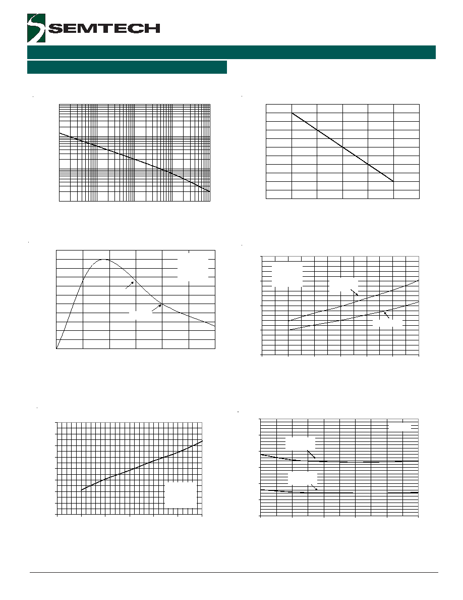
Typical Characteristics
Non-Repetitive Peak Pulse Power vs. Pulse Time
Power Derating Curve
0
10
20
30
40
50
60
70
80
90
100
110
0
25
50
75
100
125
150
Ambient Temperature - T
A
(
o
C)
% of Rated Power or I
PP
Clamping Voltage vs. Peak Pulse Current
Pulse Waveform
0
10
20
30
40
50
60
70
80
90
100
110
0
5
10
15
20
25
30
Time (µs)
Per
c
ent of I
PP
e
-t
td = I
PP
/2
Waveform
Parameters:
tr = 8µs
td = 20µs
0.01
0.1
1
10
0.1
1
10
100
1000
Pulse Duration - tp (
µs)
Peak Pulse Power - P
PP
(kW)
Junction Capacitance vs. Reverse Voltage
0
0.5
1
1.5
2
2.5
3
0
1
2
3
4
5
Reverse Voltage - V
R
(V)
Capacitance - Cj (pF)
Any I/O Pin
to Ground
Between any
two I/O pins
f = 1MHz
Forward Voltage vs. Peak Pulse Current
0
1
2
3
4
5
6
7
8
0
1
2
3
4
5
6
Peak Pulse Current - I
PP
(A)
Fo
r
w
ard Vol
t
age -
V
F
(V
)
Waveform
Parameters:
tr = 8µs
td = 20µs
5
10
15
20
25
0
1
2
3
4
5
6
Peak Pulse Current - I
PP
(A)
Clamping
Voltage - V
C
(V)
Waveform
Parameters:
tr = 8µs
td = 20µs
Pin 1, 3, 4,
or 6 to pin 2
Pin 5 to pin 2
5
2005 Semtech Corp.
www.semtech.com
PROTECTION PRODUCTS
RClamp0504P
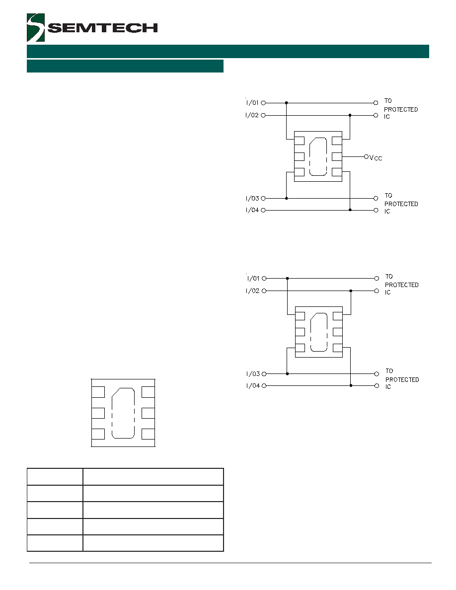
Device Connection Options for Protection of Four
High-Speed Data Lines
This device is designed to protect data lines by
clamping them to a fixed reference. When the voltage
on the protected line exceeds the reference voltage
the steering diodes are forward biased, conducting the
transient current away from the sensitive circuitry.
Data lines are connected at pins 1, 3, 4 and 6. The
center pin should be connected directly to a ground
plane. The path length is kept as short as possible to
minimize parasitic inductance. Pin 2 is not connected.
The positive reference is connected at pin 5. The
options for connecting the positive reference are as
follows:
1. To protect data lines and the power line, connect
pin 5 directly to the positive supply rail (V
CC
). In this
configuration the data lines are referenced to the
supply voltage. The internal TVS diode prevents
over-voltage on the supply rail.
2. In applications where the supply rail does not exit
the system, the internal TVS may be used as the
reference. In this case, pin 5 is not connected.
The steering diodes will begin to conduct when the
voltage on the protected line exceeds the working
voltage of the TVS (plus one diode drop).
Protection of Four Data Lines and Power Supply Line
Applications Information
Protection of Four Data Lines Using Internal TVS
Diode as Reference
1
Gnd
1
Gnd
Figure 1
Figure 1
Figure 1
Figure 1
Figure 1. Pin Conf
. Pin Conf
. Pin Conf
. Pin Conf
. Pin Configuration (T
iguration (T
iguration (T
iguration (T
iguration (Top Side Vie
op Side Vie
op Side Vie
op Side Vie
op Side View)
w)
w)
w)
w)
n
i
P
n
o
i
t
a
c
i
f
i
t
n
e
d
I
6
,
4
,
3
,
1
s
e
n
i
L
t
u
p
t
u
O
/
t
u
p
n
I
2
d
e
t
c
e
n
n
o
C
t
o
N
5
C
/
N
r
o
)l
a
n
o
it
p
O
(
V
5
b
a
T
r
e
t
n
e
C
d
n
u
o
r
G
1
Gnd
2
3
6
5
4