Synchronous Equipment Timing Source
for SONET or SDH Network Elements
ACS8510 SETS
Description
Features
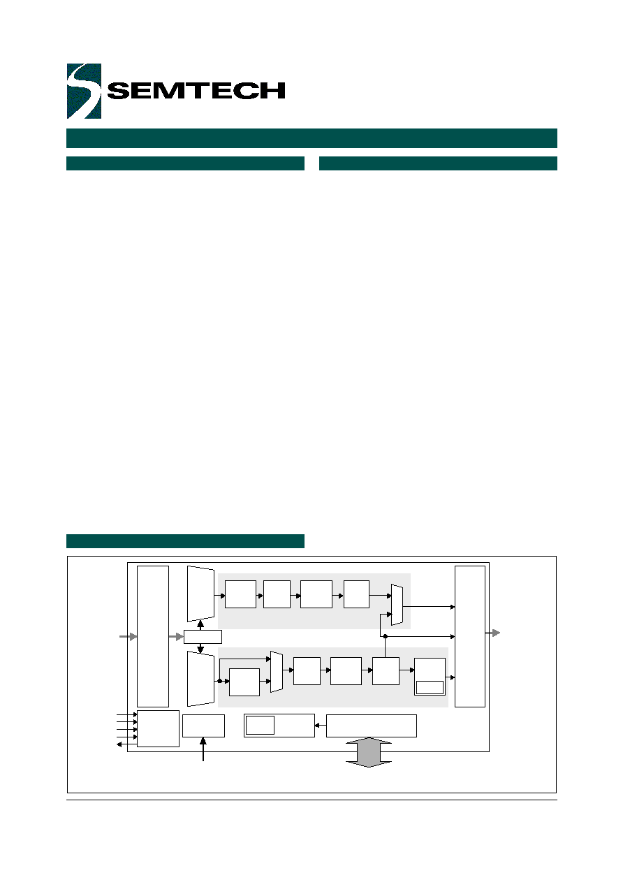
Block Diagram
The ACS8510 is a highly integrated, single-chip
solution for the Synchronous Equipment Timing
Source (SETS) function in a SONET or SDH Net-
work Element. The device generates SONET or
SDH Equipment Clocks (SEC) and frame synchro-
nization clocks. The ACS8510 is fully compliant
with the required specifications and standards.
The device supports Free-Run, Locked and
Holdover modes. It also supports all three types
of reference clock source: recovered line clock,
PDH network, and node synchronization. The
ACS8510 generates independent SEC and BITS
clocks, an 8 kHz Frame Synchronization clock
and a 2 kHz Multi-Frame Synchronization clock.
Two ACS8510 devices can be used together in a
Master/Slave configuration mode allowing sys-
tem protection against a single ACS8510 failure.
A microprocessor port is incorporated, providing
access to the configuration and status registers
for device setup and monitoring. The ACS8510
supports IEEE 1149.1 JTAG boundary scan.
ADVANCED COMMUNCIATIONS
FINAL
Revision 2.07/Jan 2001 ã2001 Semtech Corp
www.semtech.com
Suitable for Stratum 3E*, 3, 4E and 4 SONET
or SDH Equipment Clock (SEC) applications
Meets AT&T, ITU-T, ETSI and Telcordia specifi-
cations
Accepts 14 individual input reference clocks
Generates 11 output clocks
Supports Free-Run, Locked and Holdover
modes of operation
Robust input clock source quality monitoring on
all inputs
Automatic hit-less source switchover on loss
of input
Phase build-out for output clock phase conti-
nuity during input switchover and mode transi-
tions
Microprocessor interface - Intel, Motorola,
Serial, Multiplexed, EEPROM
Programmable wander and jitter tracking/
attenuation 0.1 Hz to 20 Hz
Support for Master/Slave device configuration
alignment and hot/standby redundancy
IEEE 1149.1 JTAG Boundary Scan
Single 3.3 v operation. 5 v I/O compatible
Operating temperature (ambient) -40°C to
+85°C
Available in 100 pin LQFP package
* Meets Holdover requirements, lowest bandwidth 0.1 Hz.
DPLL/Freq. S ynthesis
T
OUT0
selector
T
OUT4
selector
Chip C lock
Generator
Div ider
PFD
DPLL/F req. Synthesis
Div ider
Monitors
Dig ital
Loop
Filter
A PLL
Frequency
Dividers
M icropro cessor
Port
14 Inp ut
Reference
Source
includin g:
AM I 64/8 kHz
2 kHz
8 kHz
N x 8 kHz
1.544 MHz
2.048 MHz
6.48 MHz
19.44 MHz
25.92 MHz
38.88 MHz
51.84 MHz
77.76 MHz
155.52 M Hz
DTO
Dig ital
Loop
Filter
PFD
11 Outp ut Ports
includin g:
1.544/2.048 M Hz
3.088/4.096 M Hz
6.176/8.182 M Hz
12.352/16.384 M Hz
6.48 MHz
19.44 MHz
25.92 MHz
38.88 MHz
51.84 MHz
77.76 MHz
155.52 MHz
311.04 MHz
AM I 64/8 kHz
2 kHz MFrSy nc
8 kHz FrSy nc
Input
Ports
6xT
IN1
4xT
IN2
4xT
IN3
Output
Ports
2xT
OUT 4
7xT
OUT 0
MFrSync
FrSync
TCXO (*OCXO)
CLK
IEEE
1149.1
JTAG
T CK
TDI
TMS
T RST
TDO
Priority
T able
Register
Set
Priority
T able
Register
Set
DTO
MFrSync

Revision 2.07/Jan 2001 ã2001 Semtech Corp
www.semtech.com
2
ACS8510 SETS
ADVANCED COMMUNCIATIONS
FINAL
Table of Contents
Pin diagram................................................................................................................................................3
Pin descriptions.........................................................................................................................................4
Functional description...............................................................................................................................7
Electrical specification............................................................................................................................45
Microprocessor interface timing characteristics.......................................................................................56
Package information................................................................................................................................65
Application information............................................................................................................................67
Revision History.......................................................................................................................................68
Order information....................................................................................................................................69
Local oscillator clock..........................................................................................................................................................8
Input Interfaces..................................................................................................................................................................8
Over voltage protection.......................................................................................................................................................8
Input reference clock ports................................................................................................................................................9
Input wander and jitter tolerance...................................................................................................................................11
Output clock ports...........................................................................................................................................................13
Output wander and jitter..................................................................................................................................................14
Phase variation.................................................................................................................................................................16
Phase build-out.................................................................................................................................................................17
Microprocessor interface................................................................................................................................................17
Interrupt enable and clear...............................................................................................................................................19
Register map description.................................................................................................................................................21
Register map description.................................................................................................................................................25
Selection of input reference clock source.....................................................................................................................33
Clock quality monitoring..................................................................................................................................................34
Activity monitoring...........................................................................................................................................................35
Modes of operation..........................................................................................................................................................38
Protection facility.............................................................................................................................................................39
JTAG..............................................................................................................................................................................42
Power on reset - PORB.....................................................................................................................................................42
Absolute maximum range...............................................................................................................................................45
Operating conditions.......................................................................................................................................................45
TTL DC characterisitics...................................................................................................................................................45
PECL DC characteristics..................................................................................................................................................47
LVDS DC characteristics..................................................................................................................................................48
AMI DC characteristics....................................................................................................................................................49
Jitter characteristics........................................................................................................................................................52
JTAG timing........................................................................................................................................................................55
Motorola mode..................................................................................................................................................................56
Intel mode................................................................................................................................................................58
Multiplexed mode.............................................................................................................................................................60
Serial mode.......................................................................................................................................................................62
EEPROM mode.................................................................................................................................................................64
Simplified application schematic...................................................................................................................................67