LAB
SEME
2N3810DCSM
Semelab plc.
Telephone (01455) 556565. Telex: 341927. Fax (01455) 552612.
Prelim. 1/95
DUAL HIGH GAIN
PNP TRANSISTORS IN A
HERMETICALLY SEALED
CERAMIC SURFACE MOUNT PACKAGE
FOR HIGH RELIABILITY APPLICATIONS
FEATURES
· HERMETIC CERAMIC SURFACE
MOUNT PACKAGE
· CECC SCREENING OPTIONS
· SPACE QUALITY LEVELS OPTIONS
APPLICATIONS:
Suitable for use in high gain, low noise
differential amplifier applications.
V
CBO
Collector Base Voltage
V
CEO
Collector Emitter Voltage
1
V
EBO
Emitter Base Voltage
I
C
Collector Current
P
D
Total Device Dissipation
Derate above 25°C
T
STG
Storage Temperature Range
60V
60V
5V
50mA
500mW
600mW
2.9mW / °C
3.4mW / °C
65 to 200°C
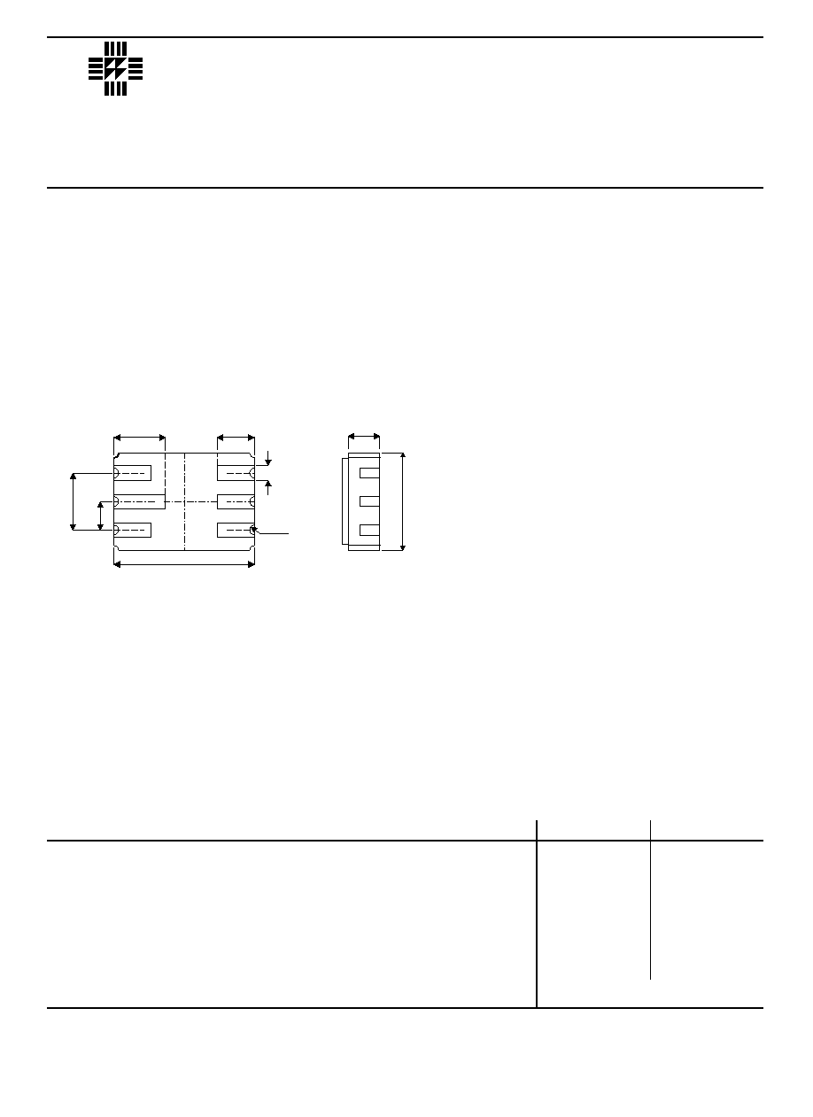
MECHANICAL DATA
Dimensions in mm (inches)
LCC2 PACKAGE
Underside View
ABSOLUTE MAXIMUM RATINGS
(T
amb
= 25°C unless otherwise stated)
PAD 1 Collector 1
PAD 2 Base 1
PAD 3 Base 2
PAD 4 Collector 2
PAD 5 Emitter 2
PAD 6 Emitter 1
A
2
1
3
4
5
6
6.22 ± 0.13
(0.245 ± 0.005)
2
.
54 ±
0.
13
(
0
.
10 ± 0.
005)
1.65 ± 0.13
(0.065 ± 0.005)
2.29 ± 0.20
(0.09 ± 0.008)
1.27 ± 0.13
(0.05 ± 0.005)
1.40 ± 0.15
(0.055 ± 0.006)
4.
32 ±
0.
13
(
0
.
170
±
0.
005)
0
.
64 ± 0.
08
(
0
.
025 ± 0.
003)
0.23
(0.009)
rad.
A =
NOTES
1. Base Emitter Diode Open Circuited.
EACH SIDE
TOTAL DEVICE
LAB
SEME
2N3810DCSM
Semelab plc.
Telephone (01455) 556565. Telex: 341927. Fax (01455) 552612.
Prelim. 1/95
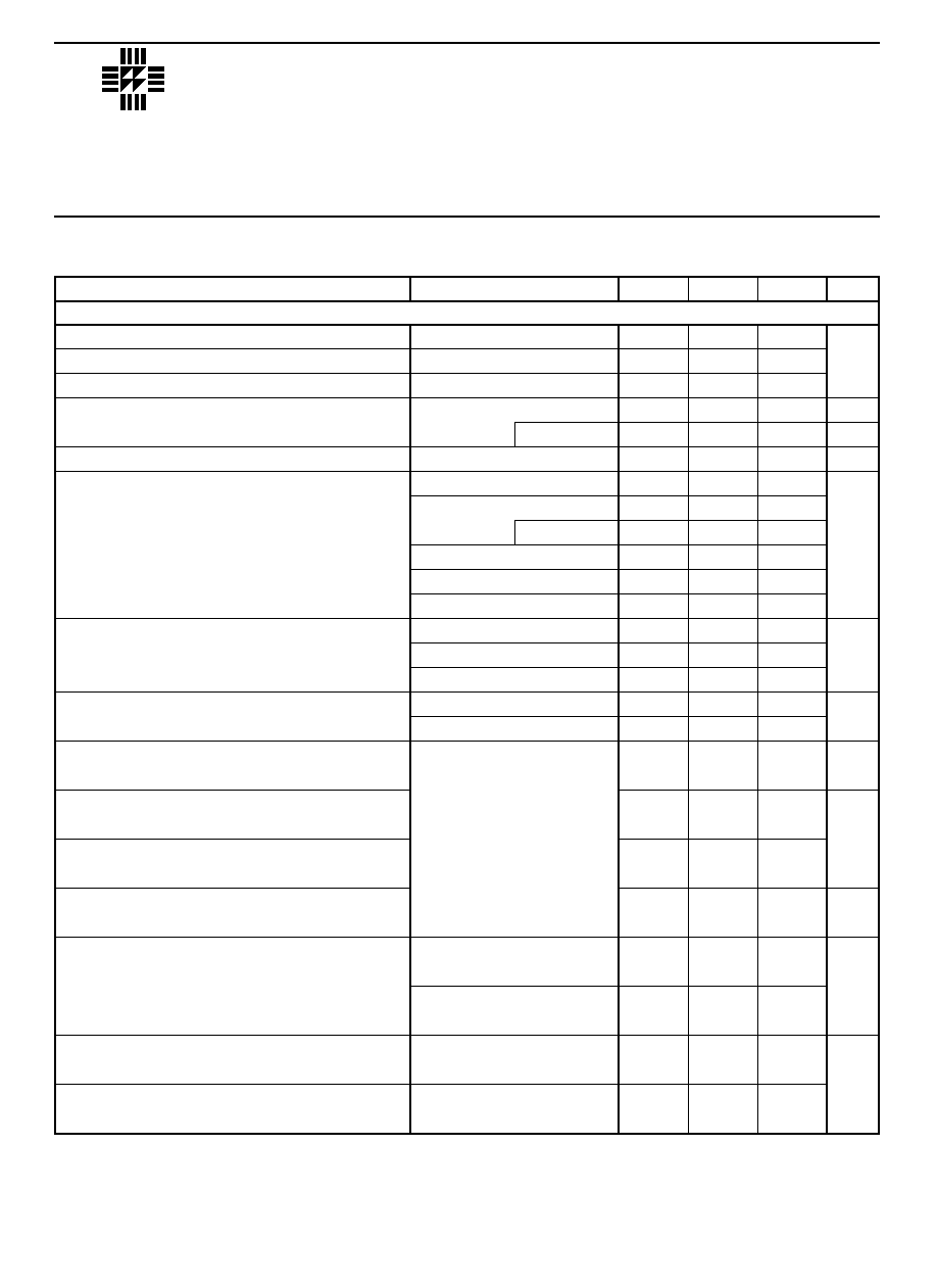
Parameter
Test Conditions
1
Min.
Typ.
Max.
Unit
V
nA
µ
A
nA
--
V
V
k
--
µ
mho
--
pF
60
60
5
10
10
20
100
150
450
75
150
450
150
450
125
0.7
0.7
0.8
0.2
0.25
3
30
150
600
25 x 10
-4
5
60
1
1
5
4
8
V
(BR)CBO
Collector Base Breakdown Voltage
V
(BR)CEO*
Collector Emitter Breakdown Voltage
V
(BR)EBO
Emitter Base Breakdown Voltage
I
CBO
Collector Cut-off Current
I
EBO
Emitter Cut-off Current
h
FE
DC Current Gain
V
BE
Base Emitter Voltage
V
CE(sat)
Collector Emitter Saturation Voltage
h
ie
Small Signal Common Emitter
Input Impedance
h
fe
Small Signal Common Emitter
Current Gain
h
re
Small Signal Common Emitter
Reverse Voltage Gain
h
oe
Small Signal Common Emitter
Output Admittance
|h
fe
|
Small Signal Common Emitter
Current Gain
C
obo
Common Base Open Circuit
Output Capacitance
C
ibo
Common Base Open Circuit
Input Capacitance
I
C
= 10
µ
A
I
E
= 0
I
C
= 10mA
I
B
= 0
I
E
= 10
µ
A
I
C
= 0
V
CB
= 50V
I
E
= 0
T
A
= 150°C
V
EB
= 4V
I
C
= 0
I
C
= 10
µ
A
V
CE
= 5V
I
C
= 100
µ
A
V
CE
= 5V
T
A
= 55°C
I
C
= 500
µ
A
V
CE
= 5V
I
C
= 1mA
V
CE
= 5V
I
C
= 10mA
V
CE
= 5V *
I
C
= 100
µ
A
V
CE
= 5V
I
B
= 10
µ
A
I
C
= 100
µ
A
I
B
= 100
µ
A
I
C
= 1mA
I
B
= 10
µ
A
I
C
= 100
µ
A
I
B
= 100
µ
A
I
C
= 1mA
V
CE
= 10V
I
C
= 1mA
f = 1kHz
V
CE
= 5V
I
C
= 500
µ
A
f = 30MHz
V
CE
= 5V
I
C
= 1mA
f = 100MHz
V
CB
= 5V
I
E
= 0
f = 100kHz
V
EB
= 0.5V
I
C
= 0
f = 100kHz
ELECTRICAL CHARACTERISTICS
(Tamb = 25°C unless otherwise stated)
NOTES
* Pulse Test: t
p
= 300
µ
s,
2%.
1) Terminals not under test are open circuited under all test conditions.
INDIVIDUAL TRANSISTOR CHARACTERISTICS
LAB
SEME
2N3810DCSM
Semelab plc.
Telephone (01455) 556565. Telex: 341927. Fax (01455) 552612.
Prelim. 1/95
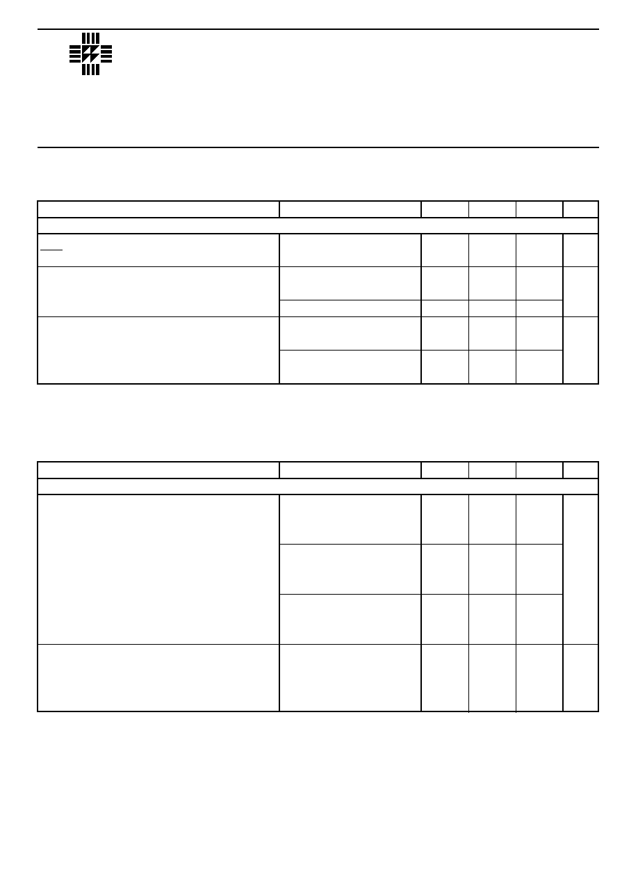
ELECTRICAL CHARACTERISTICS
(Tamb = 25°C unless otherwise stated)
NOTES
1) Terminals not under test are open circuited under all test conditions.
2) The lower of the two readings is taken as h
FE1
.
3) Average noise figure is measured in an amplifier with response down 3dB at 10Hz and 10 kHz and a high frequency
rolloff of 6dB / octave.
Parameter
Test Conditions
Min.
Typ.
Max.
Unit
--
mV
mV
0.9
1
5
3
0.8
1
h
FE1
Static Forward Current Gain
h
FE2
Balance Ratio
|V
BE1
V
BE2
|
Base Emitter Voltage
Differential
|
(V
BE1
V
BE2
)
T
A
|
Base Emitter Voltage
Differential
V
CE
= 5V
I
C
= 100
µ
A
See Note 2.
V
CE
= 5V
I
C
= 10
µ
A to 10mA
V
CE
= 5V
I
C
= 100
µ
A
V
CE
= 5V
I
C
= 100
µ
A
T
A1
= 25°C
T
A2
= 55°C
V
CE
= 5V
I
C
= 100
µ
A
T
A1
= 25°C
T
A2
= 125°C
TRANSISTOR MATCHING CHARACTERISTICS
OPERATING CHARACTERISTICS
(Tamb = 25°C unless otherwise stated)
Parameter
Test Conditions
1
Min.
Typ.
Max.
Unit
dB
dB
7
3
2.5
3.5
F
Spot Noise Figure
_
F
Average Noise Figure
V
CE
= 10V
I
C
= 100
µ
A
R
G
= 3k
f = 100Hz
Noise Bandwidth = 20Hz
V
CE
= 10V
I
C
= 100
µ
A
R
G
= 3k
f = 1kHz
Noise Bandwidth = 200Hz
V
CE
= 10V
I
C
= 100
µ
A
R
G
= 3k
f = 10kHz
Noise Bandwidth = 2kHz
V
CE
= 10V
I
C
= 100
µ
A
R
G
= 3k
Noise Bandwidth = 15.7kHz
See Note 3.
INDIVIDUAL TRANSISTOR CHARACTERISTICS

LAB
SEME
2N3810DCSM
Semelab plc.
Telephone (01455) 556565. Telex: 341927. Fax (01455) 552612.
Prelim. 1/95
THERMAL INFORMATION
0
25
50
75
100
125
150
175
200
0.0
0.1
0.2
0.3
0.4
0.5
0.6
0.7
0.8
T Free Air Temperature (°C)
A
P
M
a
x
i
m
u
m
C
o
nt
i
nuo
us
D
i
ssi
pat
i
o
n
(
W
)
T
T O TA L D EVIC E
EAC H
TR AN SISTO R