
Overview
The LC895926 is a CD-R IC that provides a wide range of
functions including CD-ROM decoding (including ECC)
and encoding, subcode encoding and decoding, CD
encoding, ATIP decoding and CLV servo, and a SCSI
interface that includes the register block.
Features
Ę ECC and EDC correction/addition for CD-ROM data
(during decoding and encoding)
Ę Subcode decoding/encoding complete with error
detection and error correction
Ę ATIP decoding and CRC checking for both encoding
and decoding
Ę CLV servo control using ATIP data during encoding
Ę CIRC code insertion and EFM modulation during
encoding
Ę Access to buffer RAM from microcontroller via
LC895926
Ę Built-in SCSI interface
Ę Speeds of 24
ū
for decoding and 12
ū
for encoding
Ę Transfers speeds of 10 megabytes/s (synchronous) and 5
megabytes/s (asynchronous) with 16-bit 50-ns EDO-
DRAMs
Ę Buffer RAM sizes between 1 and 32 megabits (using 16-
bit EDO-DRAMs)
Ę User control over sizes of CD main channel, C2 flag,
and subcode areas in buffer RAM
Ę Built-in batch transfer function for transferring entire
CD main channel, C2 flag, or subcode area in a single
operation.
Ę Built-in multiblock transfer function for transferring
multiple blocks in a single operation.
Ę Automatic sequencing of encoding and decoding
processing for a reduced processing load on the system
microcontroller.
Package Dimensions
unit: mm
3153A-QFP160E
CMOS IC
51398HA (OT) No. 5829-1/7
SANYO: QIP160E
[LC895926]
SANYO Electric Co.,Ltd. Semiconductor Bussiness Headquarters
TOKYO OFFICE Tokyo Bldg., 1-10, 1 Chome, Ueno, Taito-ku, TOKYO, 110-8534 JAPAN
CD-R Encoder/Decoder IC with Built-in SCSI Interface
LC895926
Ordering number : EN5829A
No. 5829-2/7
LC895926
Parameter
Symbol
Conditions
Ratings
Unit
Maximum power supply voltage
V
DD
max
Ł0.3 to +7.0
V
I/O voltage
V
I
, V
O
Ł0.3 to V
DD
+0.3
V
Allowable power dissipation
Pd max
Ta
70░C
600
mW
Operating temperature
Topr
Ł30 to +70
░C
Storage temperature
Tstg
Ł55 to +125
░C
Solder resistance (Pins only)
10 seconds
260
░C
Specifications
Absdute Maximum Ratings
at Ta = 25░C, V
SS
= 0 V
Parameter
Symbol
Conditions
Ratings
Unit
min
typ
max
Input high level voltage
V
IH
TTL levels, for pins (1) and (6)
2.2
V
Input low level voltage
V
IL
0.8
V
Input high level voltage
V
IH
TTL levels, for pin (4), with pull-up resistors
2.2
V
Input low level voltage
V
IL
0.8
V
Input high level voltage
V
IH
TTL levels, for pins (0) and (7), with Schmitt inputs
2.5
V
Input low level voltage
V
IL
0.6
V
Output high level voltage
V
OH
I
OH
= Ł2 mA, for pin (3)
V
DD
-- 2.1
V
Output low level voltage
V
OL
I
OL
= 2 mA, for pin (3)
0.4
V
Output high level voltage
V
OH
I
OH
= Ł2 mA, for pins (2), (4), and (6)
V
DD
-- 2.1
V
Output low level voltage
V
OL
I
OL
= 2 mA, for pins (2), (4), and (6)
0.4
V
Output high level voltage
V
OH
I
OH
= Ł48 mA, for pin (7)
V
DD
-- 2.1
V
Output low level voltage
V
OL
I
OL
= 48 mA, for pin (7)
0.4
V
Output low level voltage
V
OL
I
OL
= 2 mA, for pin (5)
0.4
V
Input leak current
I
IL
V
I
= V
SS
, V
DD
, for pins (0), (1), (6), and (7)
Ł10
+10
ĄA
Pull-up resistance
R
UP
For pins (4) and (5)
40
80
160
k
DC Characteristics
at Ta = Ł30 to +70░C, V
SS
= 0 V, V
DD
= 4.5 to 5.5 V
Parameter
Symbol
3.3V
5V
Unit
min
typ
max
min
typ
max
Power supply voltage
V
DD
3.0
3.3
3.6
4.5
5.0
5.5
V
Input voltage range
V
IN
0
V
DD
0
V
DD
V
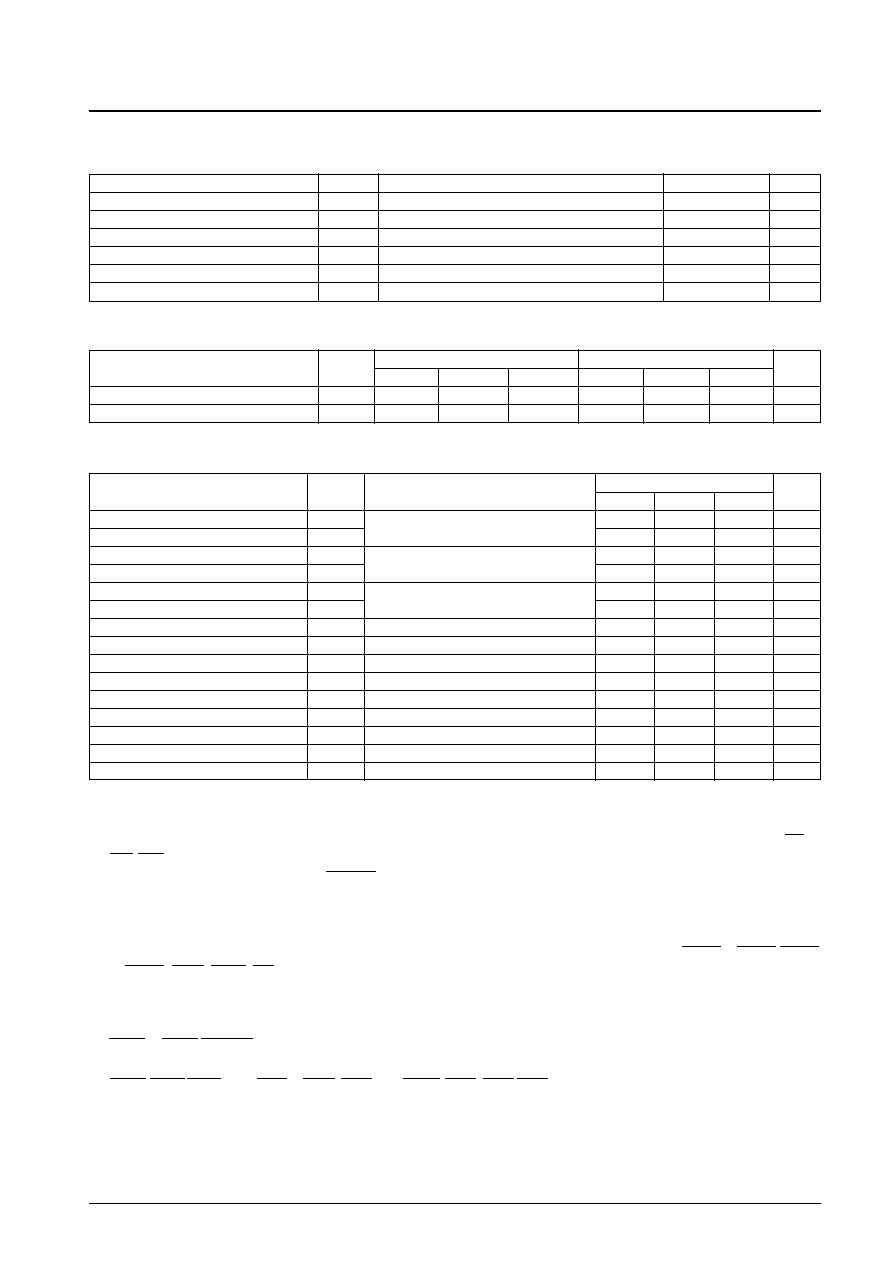
Allowable Operating Ranges
at Ta = Ł30 to +70░C, V
SS
= 0 V
The pins above refer to the following groups.
Input
(0) BCK, BICLKIN, BIDATAI, C2PO, LOCKIN, LRCK, PLLOUTIN, ROUGH, SBSO, SCOR, SDATA, WFCK, CS,
RD, WR
(1) SUA0 to SUA7, TEST0 to TEST6, RESET
Output
(2) CLV
+
, CLV
Ł
, FSW
(3) EFM, EFMG, EFMGATE0 to EFMGATE3, EXCK, LOCK, MON, RA0 to RA9, SUBSYNC, CAS0 to CAS1, RAS0
to RAS1, LWE, UWE, OE
Input
(4) D0 to D7, IO0 to IO15
(5) INT0 to INT1, SWAIT
(6) ATIPSYNC, Reserve0 to Reserve7
(7) ACK, ATN, BSY, C/D, DB0 to DB7, DBP, I/O, MSG, REQ, RST, SEL
Note: The XTAL0, XTAL1, XTALCK0, and XTALCK1 pins are not included in these DC characteristic specifications.

*1 WFCK, SBSO, SCOR
*2 BCK, SDATA, LRCK, C2PO
*3 DB0 to DB7, DBP, BSY, MSG, SEL, RST, REQ, I/O, C/D
*4 ACK, ATN
*6 RD, WR, SUA0 to SUA7, CS
*7 D0 to D7
*8 IO0 to IO15
*9 RA0 to RA9, RAS0, RAS1, CAS0, CAS1, OE, UWE, LWE
*10 PLLOUTIN, ROUGH, LOCKIN, BICLKIN, BIDATAIN
*11 LOCK, CLV
+
(MDP), CLV
Ł
(MDS), MON, FSW
*12 SUBSYNC, EFM, EFMG, EFMGATE0 to EFMGATE3
Block Diagram
No. 5829-3/7
LC895926
Sub-code I/F
de-interleave/interleave

Pin Descriptions
No. 5829-4/7
LC895926
Type: I: Input pin, O: Output pin, B: Bidirectional pin, P: Power supply pin, N: No connection pin
Pin Number
Pin Name
Type
Description
1
V
SS
P
2
XTALCK0
I
Xtal oscillator circuit input pin (17.2872 MHz)
3
XTAL0
O
Xtal oscillator circuit output pin
4
TEST0
I
Test pin (connect to V
SS
)
5
RESET
I
Reset pin
6
V
DD
P
5V
7
SUBSYNC
O
Subcode synchronization signal output pin
8
EFMG
O
EFM output gate signal output pin
9
EFM
O
EFM signal output pin
10
EFMGATE0
O
11
EFMGATE1
O
EFM pulse width detection gate signals
12
EFMGATE2
O
13
EFMGATE3
O
14
TEST1
I
Test pin (connect to V
SS
)
15
Reserve0
B
16
Reserve1
B
17
Reserve2
B
Reserved for future expansion (connect to V
SS
if unused.)
18
Reserve3
B
19
Reserve4
B
20
V
DD
P
3.3V
21
V
SS
P
22
Reserve5
B
23
Reserve6
B
Reserved for future expansion (connect to V
SS
if unused.)
24
Reserve7
B
25
TEST2
I
Test pin (connect to V
SS
)
26
LOCKIN
I
CD decoder lock signal input pin
27
LOCK
O
CLV servo lock monitor pin
28
PLLOUTIN
I
Wobble signal carrier clock input pin
29
V
SS
P
30
ROUGH
I
Rough CLV servo wobble signal input pin
31
ATIPSYNC
B
ATIP synchronization signal I/O pin
32
BICLKIN
I
Biphase data transfer clock input pin
33
BIDATAI
I
Biphase data input pin
34
V
DD
P
3.3V
35
V
SS
P
36
CLV
+
(MDP)
O
37
CLV
Ł
(MDS)
O
CLV servo signal output pin
38
MON
O
39
FSW
O
40
V
DD
P
5V
41
V
SS
P
Continued on next page.

No. 5829-5/7
LC895926
Continued from preceding page.
Type: I: Input pin, O: Output pin, B: Bidirectional pin, P: Power supply pin, N: No connection pin
Pin Number
Pin Name
Type
Description
42
IO0
B
43
IO1
B
44
IO2
B
Data signal pins for ROM encoder/decoder DRAM, with pull-up resistors
45
IO3
B
46
IO4
B
47
IO5
B
48
V
DD
P
5V
49
IO6
B
50
IO7
B
Data signal pins for ROM encoder/decoder DRAM, with pull-up resistors
51
IO8
B
52
IO9
B
53
V
SS
P
54
IO10
B
55
IO11
B
56
IO12
B
Data signal pins for ROM encoder/decoder DRAM, with pull-up resistors
57
IO13
B
58
IO14
B
59
IO15
B
60
V
DD
P
3.3V
61
V
SS
P
62
RA0
O
63
RA1
O
64
RA2
O
65
RA3
O
Address signal pins for ROM encoder/decoder DRAM
66
RA4
O
67
RA5
O
68
RA6
O
69
V
SS
P
70
RA7
O
71
RA8
O
Address signal pins for ROM encoder/decoder DRAM
72
RA9
O
73
RAS0
O
RAS signal pins for ROM encoder/decoder DRAM
74
RAS1
O
75
CAS0
O
CAS signal pins for ROM encoder/decoder DRAM
76
CAS1
O
77
OE
O
Output enable signal pin for ROM encoder/decoder DRAM
78
UWE
O
Upper write enable signal pin for ROM encoder/decoder DRAM
79
LWE
O
Lower write enable signal pin for ROM encoder/decoder DRAM
80
V
DD
P
5V
81
V
SS
P
82
DB0
B
SCSI pins
83
DB1
B
84
V
DD
P
3.3V
85
DB2
B
SCSI pins
86
DB3
B
87
V
SS
P
88
DB4
B
SCSI pins
89
DB5
B
Continued on next page.