
Overview
The LC895297 is a single-chip CD-ROM decoder and
CD-DSP system that supports full CAV 20
×
operation and
includes a built-in ATA-PI (IDE) interface.
Functions
· Full CAV 20
×
CD-DSP and CD-ROM decoder
functions with built-in ATA-PI (IDE) interface
Features
[CD-ROM Decoder and ATA-PI (IDE) Interface Blocks]
· Full CAV 20
×
operation
· ATA-PI (IDE) interface
· Supports the use of EDO DRAM.
· Supports the use of up to 4 Mbits of buffer RAM.
· The user can set up arbitrary CD main channel and C2
flag areas in buffer RAM.
· Batch transfer function (function that automatically
transfers the CD main channel and C2 flag data in a
single operation.)
· Multi-block transfer function (function that
automatically transfers multiple blocks in a single
operation.)
· DVD ECC interface
· Intelligent functions
[CD-DSP Block]
· The IC inputs a high-frequency signal, slices that signal
at the correct level, converts that result to an EFM coded
signal, and compares the phase with that of the built-in
VCO.
· Uses an external 16.9344-MHz crystal element to
generate a standard clock and to correctly generate the
required internal timings.
· Performs frame synchronization, signal detection,
protection, and insertion, and assures stable data
readout.
· Demodulates the EFM coded signal to produce 8-bit
symbol data.
· After applying a CRC check to the subcode Q signal,
outputs that signal to a microprocessor over a parallel
I/O channel.
· Performs unscrambling and de-interleaving to reorder
the demodulated EFM signal in the prescribed manner.
· Performs error code detection and correction, and flag
processing. (C1: dual errors, C2: four errors)
· Sets the C2 flags based on the C1 flags and a C2 check,
and performs interpolation or muting depending on the
C2 flags. Adopts a 2-point interpolation circuit, and
converges the signal to the muting level if the C2 flags
indicate over 2 consecutive uncorrectable errors.
· Accepts the input of commands from a control
microprocessor over an 8-bit parallel interface. Supports
track jump, disc motor start/stop, muting on/off, and
track counting commands.
· Can perform arbitrary track counts.
· Includes CAV audio functions.
· Adopts zero-cross muting.
· Includes 8
×
oversampling digital filters.
· D/A converter with PWM output.
· Includes independent left and right channel digital
attenuators.
· Provides digital deemphasis.
· Supports bilingual functions.
Package Dimensions
unit: mm
3230-SQFP176
CMOS LSI
22898HA (OT) No. 5785-1/9
Preliminary
SANYO: SQFP176
[LC897297]
SANYO Electric Co.,Ltd. Semiconductor Bussiness Headquarters
TOKYO OFFICE Tokyo Bldg., 1-10, 1 Chome, Ueno, Taito-ku, TOKYO, 110-0005 JAPAN
Full CAV 20
×
CD-ROM Decoder with
Built-in ATA-PI (IDE) Interface and CD-DSP
LC895297
Ordering number : EN
*
5785

No. 5785-2/9
LC895297
Parameter
Symbol
Conditions
Ratings
Unit
Maximum supply voltage
V
DD
max
0.3 to +7.0
V
Input and output voltage
V
I
, V
O
0.3 to V
DD
+0.3
V
Allowable power dissipation
Pd max
Ta
70°C
*
1
500
mW
Operating temperature
Topr
30 to +70
°C
Storage temperature
Tstg
55 to +125
°C
Soldering conditions (pins only)
10s
235
°C
Input and output current
I
I
, I
O
Per individual input or output cell
±20
mA
Note 1: Applications that use this IC must adopt heat dissipation measures, such as the insertion of a thermally conductive sheet.
Specifications
Absolute Maximum Ratings
at Ta = 25°C, V
SS
= 0 V
Parameter
Symbol
Conditions
Ratings
Unit
min
typ
max
[Input and Output Cell Power Supply]
Supply voltage
V
DD
4.5
5.0
5.5
V
Input voltage range
V
IN
0
V
DD
V
[Internal Cell Power Supply]
Supply voltage
V
DD
3.9
4.0
4.1
V
Input voltage range
V
IN
0
V
DD
V
Allowable Operating Ranges
at Ta = 30 to +70°C, V
SS
= 0 V
Parameter
Symbol
Conditions
Ratings
Unit
min
typ
max
Input high-level voltage
V
IH
TTL levels. Applicable pins: (10) and (13)
2.2
V
Input low-level voltage
VIL
0.8
V
Input high-level voltage
V
IH
TTL levels. Applicable pins: (1)
2.2
V
Input low-level voltage
V
IL
Pull-up resistor included.
0.8
Input high-level voltage
V
IH
TTL levels. Applicable pins: (2), (3), and (15)
2.4
V
Input low-level voltage
V
IL
Schmitt inputs.
0.8
V
Input high-level voltage
V
IH
CMOS levels: Applicable pins: (14)
0.7 V
DD
V
Input low-level voltage
V
IL
0.3 V
DD
V
Input high-level voltage
V
IH
CMOS levels: Applicable pins: (4)
0.8 V
DD
V
Input low-level voltage
V
IL
Schmitt inputs.
0.2 V
DD
V
Output high-level voltage
V
OH
I
OH
= 2 mA: Applicable pins: (5), (1), (9),
V
DD
2.1
V
(10), and (15)
Output low-level voltage
V
OL
I
OL
= 2 mA: Applicable pins: (5), (1), (9),
0.4
V
(10), and (15)
Output high-level voltage
V
OH
I
OH
= 4 mA: Applicable pins: (3) and (6)
V
DD
2.1
V
Output low-level voltage
V
OL
I
OL
= 24 mA: Applicable pins: (3) and (6)
0.4
V
Output low-level voltage
V
OL
I
OL
= 2 mA: Applicable pins: (7) and (11)
0.4
V
Output low-level voltage
V
OL
I
OL
= 24 mA: Applicable pins: (12)
0.4
V
Input leakage current
I
IL
V
I
= V
SS
, V
DD
: Applicable pins: (2), (3), (4),
10
+10
µA
(10), and (15)
Output leakage current
I
OZ
In high-impedance output mode: Applicable
10
+10
µA
pins: (3), (6), (7), (9), (10), (12), and (15)
Pull-up resistance
R
UP
Applicable pins: (1) and (11)
40
80
160
k
Electrical Characteristics
at Ta = 30 to +70°C, V
SS
= 0 V, V
DD
= 4.5 to 5.5 V
The applicable pin sets are as follows:
[INPUT]
(2) ZRESET, ZDMACK, ZHRST, DA0to DA2, ZCS1FX, ZCS3FX, ZDIOR, ZDIOW, FG
(4) ZCSCTRL, ZCS, ZRD, ZWR, HFL, TES
(14) DEFI
(13) SUA0 o SUA6
[OUTPUT]
(6) DMARQ, HINTRQ
(5) RA0 to RA8, ZRAS0, ZCAS0, ZOE, ZUWE, ZLWE, C2F, ROMXA, FSX, EFLG, PCK, FSEQ, TOFF, TGL, 4.2M, WRQ, RWC, COIN, ZCQCK, RCHP,
RCHN, LCHP, LCHN
(7) ZRSTCPU, ZRSTIC
(9) JP
+
, JP
, SPO
(11) ZINT0, ZINT1, ZSWAIT
(12) IORDY, ZIOCS16
Continued on next page.
No. 5785-3/9
LC895297
[INOUT]
(1) D0 to D7, IO0 to IO15
(3) DD0 to DD15, ZDASP, ZPDIAG
(10) IOP0 to IOP7
(15) DRESP, DREQ
Note: XTAL, XTALCK, R0, VCNT0, PDO0, R1, VCNT1, PO11, PO21, BSN1, R2, VCNT2, PO12, PO22, and BSN2
The above pins are not covered by the electrical characteristics.
The 1-bit D/A converter block pins are only measured using a logic tester; no analog measurements are performed.
Continued from preceding page.
Parameter
Symbol
Conditions
Ratings
Unit
min
typ
max
Input high-level voltage
V
IH
Micro-signal amplifier. Applicable pins: EFMI
3.2
V
Input low-level voltage
V
IL
1.8
V
Output high-level voltage
V
OH
I
OH
= 4 mA. Applicable pins:
V
DD
2.1
V
EFMO and ZEFMO
Output low-level voltage
V
OL
I
OL
= 4 mA. Applicable pins:
0.4
V
EFMO and ZEFMO
Input leakage current
I
IL
V
I
= V
SS
, V
DD
: Applicable pins: EFMI
10
+10
µA
Output leakage current
I
OZ
In high-impedance mode: Applicable pins:
10
+10
µA
EFMO and ZEFMO
Electrical Characteristics
at Ta = 30 to +70°C, V
SS
= 0 V, V
DD
= 4.5 to 5.5 V
EFM Input and Output Signals
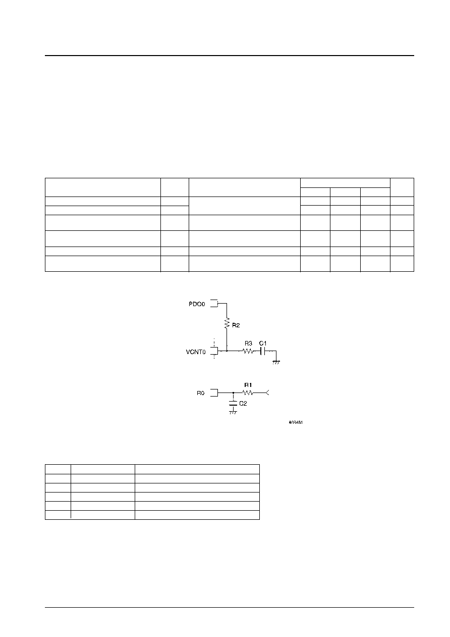
External Clock Generator PLL Circuit
Figure 1 PLL Circuit
While the circuit structure is fixed, the values of the components will vary with the circuit board capacitance and other application circuit parameters.
Symbol
Currently used value
Notes
R1
7.5 k
VCO adjustment resistor
R2
10 k
Low-pass filter resistor
R3
200
Low-pass filter phase compensation resistor
C1
0.1 µF
Low-pass filter capacitor
C2
0.1 µF
VCO bias stabilization capacitor
No. 5785-4/9
LC895297
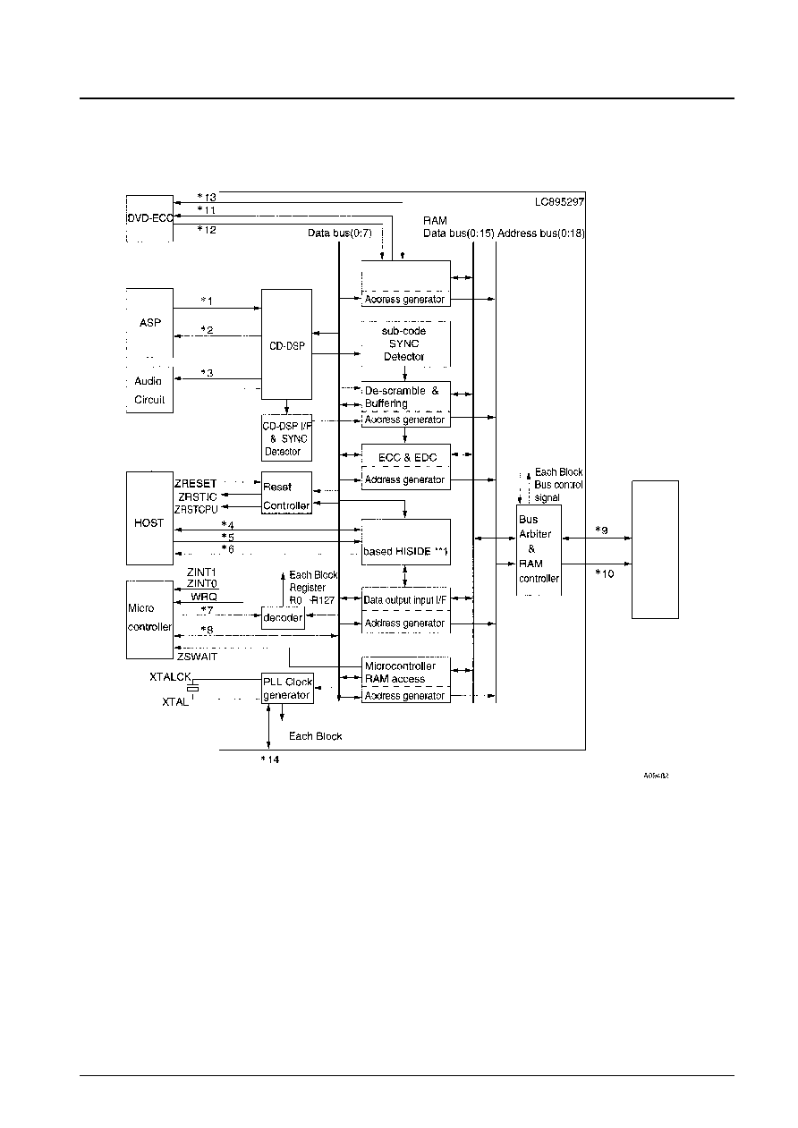
Block Diagram
*
1 DEFI, EFMI, HFL, TES
*
2 4.2M, EFMO, PCK, FSEQ, TOFF, TGL, JP
+
, JP
, RWC, COIN, ZCQCK
*
3 RCHP, RCHN, LCHP, LCHN
*
4 DD0 to DD15, ZDASP, ZPDIAG
*
5 ZCS1FX, ZCS3FX, DA0 to DA2, ZDIOR, ZDIOW, ZDMACK, ZHRST
*
6 DMARQ, HINTRQ, ZIOCS16, IORDY
*
7 ZRD, ZWR, ZCS, ZCSCTRL, SUA0 to SUA6
*
8 D0 to D7
*
9 IO0 to IO15
*
10 RA0 to RA8, ZRAS0, ZCAS0, ZOE, ZUWE, ZLWE
*
11 DREQ
*
12 DRESP
*
13 IOP0 to IOP7
*
14 R0, VCNT0, PDO0
**
1 HISIDE (WD25C32) is made by WESTERN DIGITAL
DVD interface
IDE interface
External
buffer
RAM
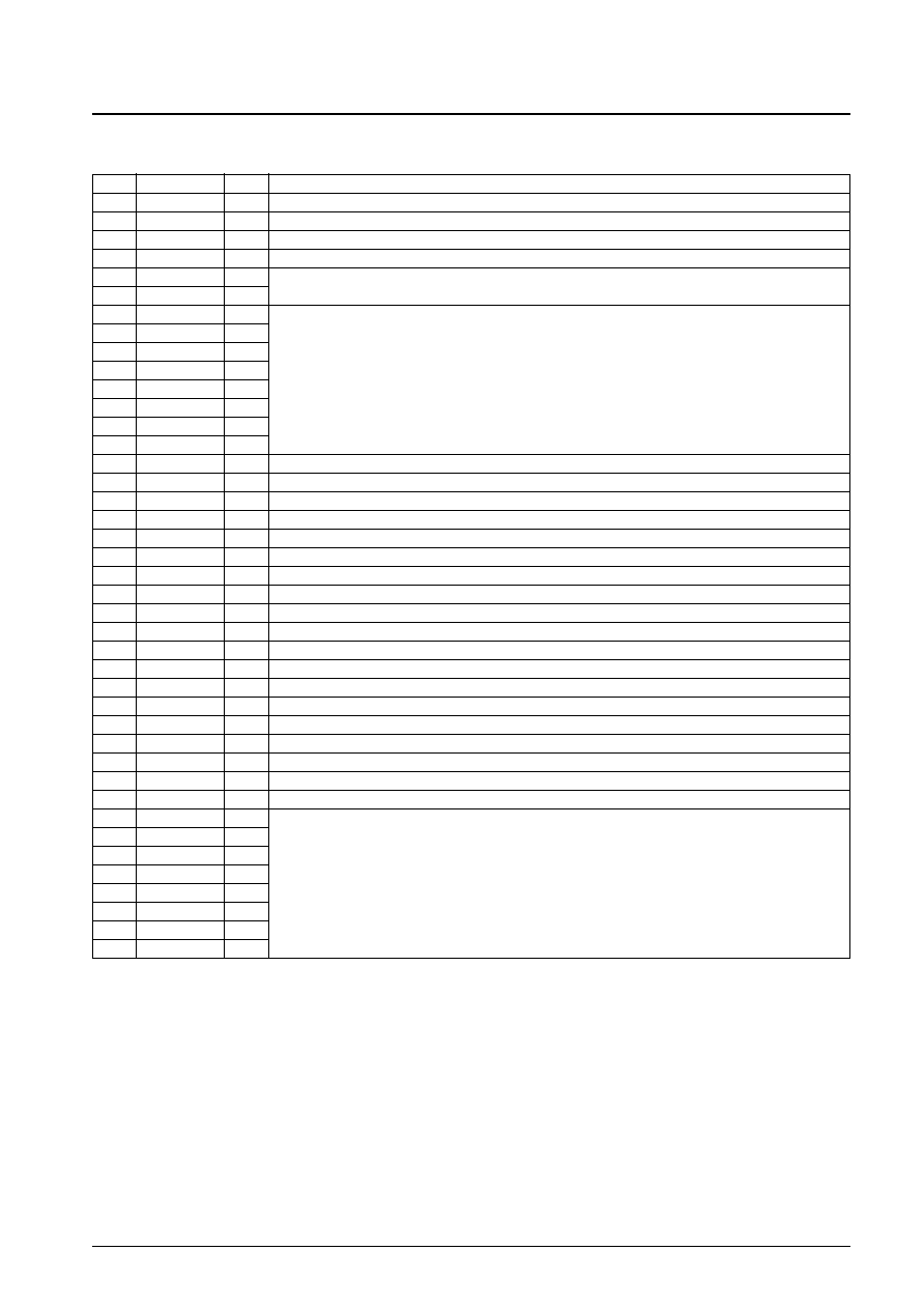
Pin Functions
I : Input pin, O: Output pin, B : Bidirectional pin, P: Power supply pin, NC: Not connected
No. 5785-5/9
LC895297
Pin No.
Pin name
Type
Function
1
AV
SS0
P
2
R0
I
VCO bias resistor connection
3
VCNT0
I
VCO control voltage input
4
PDO0
O
Charge pump output
5
TEST0
I
Test pins
6
TEST1
I
7
IOP0 (HDB7)
B
8
IOP1 (HDB6)
B
9
IOP2 (HDB5)
B
10
IOP3 (HDB4)
B
General-purpose I/O ports
11
IOP4 (HDB3)
B
These pins are used for DVD ECC data input when the DVD interface is used.
12
IOP5 (HDB2)
B
13
IOP6 (HDB1)
B
14
IOP7 (HDB0)
B
15
V
DD2
P
4.0 V
16
TEST3
I
Test pin
17
TEST4
I
Test pin
18
DRESP
I
DVD ECC data latch signal input
19
DREQ
O
DVD ECC data request output
20
RCHP
O
1-bit D/A converter right channel P output
21
RCHN
O
1-bit D/A converter right channel N output
22
V
DD1
P
1-bit D/A converter left and right channel power supply
23
V
SS1
P
1-bit D/A converter right channel ground
24
LCHP
O
1-bit D/A converter left channel P output
25
LCHN
O
1-bit D/A converter left channel N output
26
V
SS0
P
27
XTALCK
I
Crystal oscillator circuit input (16.9344 MHz)
28
XTAL
O
Crystal oscillator circuit output
29
V
SS0
P
30
NC
31
ZRSTCPU
O
CPU reset signal output
32
ZRSTIC
O
Drive IC reset signal output
33
ZRESET
I
IC reset input
34
D7
B
35
D6
B
36
D5
B
37
D4
B
Microcontroller data signal connection.
38
D3
B
These pins include built-in pull-up resistors.
39
D2
B
40
D1
B
41
D0
B
Continued on next page.