Overview
The LC82104 converts analog image signals from a CCD
and contact image sensor to precise multi-valued image
data using a built-in 8-bit A/D converter and internal
image-processing functions. The LC82104 includes a 6-bit
reference potential setting D/A converter for the 8-bit A/D
converter and CDS function, and produces high-quality
multi-valued data by performing shading correction for all
pixels, color balance adjustment, and gamma conversion
with support for arbitrary gamma curves. It also includes a
multi-value data resolution conversion function, and thus
can support input from and output to systems with
different resolutions. Furthermore, it can perform high-
quality conversion to two-valued images from the green
signal. The LC82104 can process up to 5400 pixels by
three lines and requires no external memory whatsoever
for use in distortion correction and other processing. Thus
this IC can implement the image processing required for
color scanners, FAX, copiers, OCRs and similar
applications.
Features
· Number of pixels processed:
2700 pixels
×
3 lines
(Both bright and dark correction applied to all pixels)
5400 pixels
×
3 lines
(Only bright correction applied to all pixels)
· Processing speed:
1,200 ns/pixel maximum (3-color CCD) (When CLKIN
is 20 MHz)
400 ns/pixel maximum (CIS and black-and-white CCD)
(When CLKIN is 20 MHz)
· 8-bit A/D converter
(Includes a sensor signal timing adjustment function.)
· 6-bit D/A converter for setting the A/D converter
reference potential
· Sensor drive circuit
(Supports all types of CCD and CIS sensors)
· Digital CDS (Correlated double sampling)
· Digital clamp circuit
(Single-point clamping, even field clamping)
· Shading correction
(Bright correction: all-pixel correction, dark correction:
either all-pixel correction or set dark correction
attenuation data)
· Gamma correction
(Supports user-defined curves for each of R, G, and B
using 8-bit data)
· Color balance (Gain control)
· Main scan direction multi-value resolution conversion
(From 2/1 to 1/2, in units of 1/256)
· Binary coding
(Simple binary coding (slicing), and 64-level error
diffusion)
*: The green signal is converted to a binary signal.
· Memory manager
(Image data buffer memory controller)
· Fabricated in a CMOS process for 5-V single-voltage
power supply operation.
COMS IC
Ordering number : EN
*
5685
30698RM(OT) No. 5685-1/6
Preliminary
SANYO Electric Co.,Ltd. Semiconductor Bussiness Headquarters
TOKYO OFFICE Tokyo Bldg., 1-10, 1 Chome, Ueno, Taito-ku, TOKYO, 110-8534 JAPAN
Color Image Processing IC for Fax
and Scanner Applications
LC82104
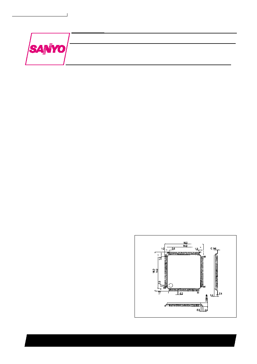
SANYO: SQFP100
[LC82104]
Package Dimensions
unit: mm
3181B-SQFP100

No. 5685-2/6
LC82104
Parameter
Symbol
Conditions
Ratings
Unit
min
typ
max
Input high-level voltage
V
IH
2.2
V
Input low-level voltage
V
IL
0.8
V
Input leakage current
I
I
V
IN
= V
DD
, V
SS
10
+10
µA
Output high-level voltage
V
OH
I
OH
= 3 mA
2.4
V
Output low-level voltage
V
OL
I
OL
= 3 mA
0.4
V
Output leakage current
I
OZ
At high-impedance
10
+10
µA
Electrical Characteristics
at Ta = 30 to +70°C, GND = 0 V, V
DD
= 4.75 to 5.25 V
Parameter
Symbol
Conditions
Ratings
Unit
Maximum supply voltage
V
DD
max
0.3 to +7.0
V
I/O voltages
V
I
, V
O
0.3 to V
DD
+ 0.3
V
Allowable power dissipation
Pd max
Ta
70 °C
400
mW
Operating temperature
Topr
30 to +70
°C
Storage temperature
Tstg
55 to +125
°C
Soldering conditions
Hand soldering: 3 seconds
350
°C
Reflow soldering: 10 seconds
235
°C
Specifications
Absolute Maximum Ratings
at Ta = 25°C, GND = 0 V
Parameter
Symbol
Conditions
Ratings
Unit
min
typ
max
Supply voltage
V
DD
4.75
5.25
V
Input voltage
V
IN
0
V
DD
V
Allowable Operating Ranges
at Ta = 30 to +70°C, GND = 0 V
Parameter
Symbol
Conditions
Ratings
Unit
min
typ
max
[D/A Converter]
Resolution
6
bit
[A/D Converter] When the low reference potential = 1.0 V, and the high reference potential = 3.0 V
Resolution
8
bit
Linearity error
±1
LSB
Differential linearity error
±1
LSB
Analog Characteristics
No. 5685-3/6
LC82104
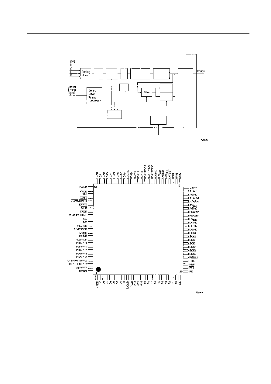
Block Diagram
Pin Assignment
Shading
correction
DRAM
6 kbit
SRAM
Digital
CDS
Gamma
correc
-tion
Multi-valued
resolution
conversion
Color balance
(gain control)
Image data
interface
Simple
bi-coding
Error
diffusion
Controller
interface signals
Controller
interface
Top view

Pin Functions
No. 5685-4/6
LC82104
typ
I
Input
B
Bidirection
NC
Not connected
O
Output
P
Power
Pin No.
Pin
I/O
Function
1
DV
DD
P
Digital system power supply
2
D7
B
3
D6
B
4
D5
B
5
D4
B
6
D3
B
7
D2
B
8
D1
B
9
D0
B
10
DGND
P
Digital system ground
11
DV
DD
P
Digital system power supply
12
A12
I
13
A11
I
14
A10
I
15
A9
I
16
A8
I
17
A7
I
18
A6
I
19
A5
I
20
A4
I
21
A3
I
22
A2
I
23
A1
I
24
A0
I
25
CS
I
CPU interface chip select
26
RD
I
CPU interface read signal
27
WR
I
CPU interface write signal
28
REF
I
DRAM refresh signal input
29
TRIG
I
External read signal input
30
RESET
I
System reset
31
SCK7
O
32
SCK6
O
33
SCK5
O
34
SCK4
O
35
SCK3
O
36
SCK2
O
37
SCK1
O
38
DGND
P
Digital system ground
39
CLKIN
I
System clock input
40
DGND
P
Digital system ground
41
DV
DD
P
Digital system power supply
42
FSAMP
O
Floating data sampling point monitor signal output
43
SSAMP
O
Signal data sampling point monitor signal output
44
AGND
P
Analog system ground
45
AV
DD
P
Analog system power supply
46
ATAPH
O
A/D converter high-level reference analog output
47
ATAPM
O
A/D converter mid-level reference analog output
48
AGND
P
Analog system ground
49
ATAPL
O
A/D converter low-level reference analog output
50
CTAP
O
Analog clamp analog output
CPU interface data bus
D7 is the MSB, D0 is the LSB.
CPU interface address bus
A12 is the MSB, A0 is the LSB.
Sensor driver signal outputs
Continued on next page.

No. 5685-5/6
LC82104
Pin No.
Pin
I/O
Function
51
GIN
I
Green sensor signal input
52
RIN
I
Red sensor signal input
53
BIN
I
Blue sensor signal input
54
ATEST
O
Analog test output (Normally left open.)
55
AV
DD
P
Analog system power supply
56
AGND
P
Analog system ground
57
DV
DD
P
Digital system power supply
58
DGND
P
Digital system ground
59
DA15/GOE
O
60
DA14/ROE
O
61
DA13/BOE
O
62
DA12
O
63
DA11
O
64
DA10
O
65
DA9
O
66
DGND
P
Digital system ground
67
DA8
O
68
DA7
O
69
DA6
O
70
DA5
O
71
DA4
O
72
DA3
O
73
DA2
O
74
DA1
O
75
DA0
O
76
DGND
P
Digital system ground
77
DV
DD
P
Digital system power supply
78
RAS
O
External memory RAS signal output
79
CAS0
O
External memory CAS signal output
80
CAS1/MWR1
O
External memory CAS0 signal output/External memory MWR1 signal
81
MWR0
O
External memory MWR0 signal output
82
MRD
O
External memory MRD signal output
83
IOWR
O
I/O write signal output
84
CLAMP/LININT
O
Clamp point monitor signal output/Line signal output
85
NC
NC
86
NC
NC
87
PD7/SD
O
DMA output/serial data output
88
PD6/SDCK
O
DMA output/serial data transfer clock
89
DV
DD
P
Digital system power supply
90
DGND
P
Digital system ground
91
PD5/SDE
O
DMA output/Serial data output valid period signal output
92
PD4/PP4
B
93
PD3/PP3
B
94
PD2/PP2
B
95
PD1/PP1
B
96
PD0/PP0
B
97
PDCK/DACK/PP5
B
Parallel data transfer clock/DMA data acknowledge signal input/general-purpose I/O port
98
PDE/DREQ/PP6
B
Parallel data output valid period signal/DMA data request signal output/general-purpose I/O port
99
MTP/PP7
B
Motor drive timing signal output/General-purpose I/O port
100
DGND
P
Digital system ground
/Green data valid period signal
/Red data valid period signal
/Blue data valid period signal
External memory address signal outputs
DA15 is the MSB, DA0 is the LSB.
External memory address signal outputs
DA15 is the MSB, DA0 is the LSB.
DMA outputs/general-purpose I/O ports
Continued from preceding page.