Ordering number :EN
*
5684
22897HA (OT) No. 5684-1/21
Overview
The LC74201E is a CMOS LSI that reduces the signal
processing functions required of a video CD decoder to a
single chip. All that it takes to make a version 1 or version
2 video CD player is the addition of a CD digital signal
processor, DRAM, an audio D/A converter, digital video
encoder, and similar components.
Features
· Incorporation of virtually almost all the functionality
required by a video CD player from the CD-ROM
decoder through to the MPEG audio and video decoders
in a single chip
· Fully automatic playback with automatic decoding
within the LSI in response to simple external commands
and the MPEG bit stream
· Special playback functions are activated by command
inputs, and do not require signal processing by the host
microcomputer
· Support for two external DRAM configurations:
4 M bits (256k
×
16 bits) or 4 M bits (256k
×
16 bits) +
1 M bit (64k
×
16 bits)
· Support for a Track 1 DRAM user area (i.e., sector
buffer) of up to 8 k bytes (4 M bits of external DRAM)
or 22 k bytes (5 M bits of external DRAM)
· Automatic synchronization of audio and video
· Built-in high-speed decoder core that supports variable-
speed video playback at up to quadruple speed. Audio
support for normal and double-speed playback.
· Internal registers that offer configuration settings for
connecting to most commercially available CD digital
signal processors and D/A converters
· Compatible with version 2 of the video CD standard.
Support for superimposition of closed caption data on
the output signal as specified in the EIA608 standard
· Support for Photo CD standard. (Base/4 and Base/16)
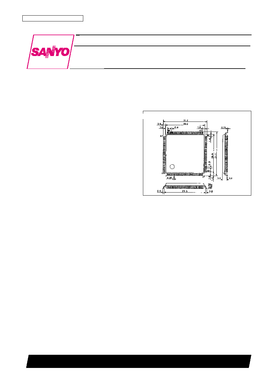
Package Dimensions
unit: mm
3182-QFP-128E
Preliminary
SANYO: QIP-128E
[LC74201E]
LC74201E
SANYO Electric Co.,Ltd. Semiconductor Bussiness Headquarters
TOKYO OFFICE Tokyo Bldg., 1-10, 1 Chome, Ueno, Taito-ku, TOKYO, 110 JAPAN
Video CD Decoder
CMOS LSI
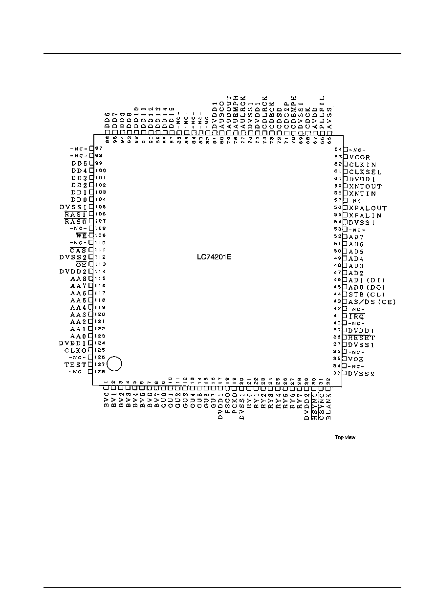
Pin Assignment
No. 5684-2/21
LC74201E
Pin Function
1. Power supply, test pin, unconnected pins
No. 5684-3/21
LC74201E
Pin No.
Symbol
I/O
Logic
Function
17
39
60
75
81
124
DV
DD
1
System power supply (3-V power supply: 3.7 to 4.0 V)
20
37
54
69
76
105
DV
SS
1
System power supply (connect to ground)
29
114
DV
DD
2
Power supply for 5-V I/O pins (5-V power supply: 5.5 ± 0.5 V)
33
112
DV
SS
2
Power supply for 5-V I/O pins (connect to ground)
NC
Unconnected pins
34, 36, 40, 42, 53, 57, 64, 82, 83, 84 pins
85, 86, 97, 98, 108, 110, 126, 128 pins
65
AV
SS
Power supply for VCO and PLL (connect to ground)
67
AV
DD
Power supply for VCO and PLL (3-V power supply: 3.7 to 4.0 V)
125
CLKO
Out
Positive
Power supply for VCO and PLL (connect to ground)
127
TEST
In
Positive
Test mode control pin (normally kept at low level)
2. Clock pins
3. Microcomputer interface
Note: AD0 to AD7 use N-channel open-drain outputs.
No. 5684-4/21
LC74201E
Pin No.
Symbol
I/O
Logic
Function
18
FSCO
Out
Positive
Subcarrier clock output (frequency = 1/4 pixel clock frequency). Tristate output using DV
DD
2 (5-V) power
supply.
19
PCKO
Out
Positive
Pixel clock output (NTSC-4fsc, PAL-4fsc, or 13.5 MHz). Tristate output using DV
DD
1 (3-V) power supply.
61
CLKSEL
In
Positive
Clock selection control input. High: 54.0-MHz clock input from pin 62 (CLKIN); Low: clock from internal
VCO oscillator.
62
CLKIN
In
Positive
54.0-MHz clock input (with built-in bias). When not used, connect to DV
DD
1 or DV
SS
1.
55
XPALIN
In
Crystal oscillator connections for PAL-4fsc oscillation circuit (4fsc = 17.734475 MHz)
58
XNTIN
In
Crystal oscillator connections for NTSC-4fsc oscillation circuit (4fsc = 14.31818 MHz)
56
XPALOUT
Out
56
59
XNTOUT
Out
66
PLLFIL
PLL filter connection
CD-DSP clock input (16.9344, 2.8224, or 2.1168 MHz)
Adjustment resistor connection for VCO oscillator circuit.
63
VCOR
68
CDCK
In
Positive
Pin No.
Symbol
I/O
Logic
Function
44
STB (CL)
In
Positive
Parallel interface: Strobe signal input for address input and data I/O.
Serial interface: Serial transfer clock signal input.
45
AD0 (DO)
I/O
Positive
Parallel interface: Address/data I/O port P0 (LSB).
Serial interface: ZPSerial data output (LSB-first input).
43
AS/DS (CE)
In
Positive
Parallel interface: Address/data select input (Low = address).
Serial interface: Serial transfer enable signal input (High = enabled).
46
AD1 (DI)
I/O
Positive
Parallel interface: Address/data I/O port P1.
Serial interface: Serial data input (LSB-first output).
41
IRQ
Out
Negative
Interrupt request signal output (N-channel open-drain output).
Parallel interface address/data I/O ports.
The interface mode is determined by the input levels at the AD4 to AD6 pins at the rising edge of the
RESET pin input.
· Serial interface: AD6:AD5:AD4 = 1:
*
:
*
(
*
= Don't care)
· Parallel interface: AD6:AD5:AD4 = 0:1:0
AD7: Parallel interface address/data I/O port P7 (MSB).
System reset input (Hysteresis input; built-in pull-up resistor).
38
REST
In
Negative
47
AD2
I/O
Positive
48
AD3
I/O
Positive
49
AD4
I/O
Positive
50
AD5
I/O
Positive
51
AD6
I/O
Positive
52
AD7 (MBS)
I/O
Positive
4. CD interfaces
5. Audio D/A converter interface
Note:The four pins making up the audio D/A converter interface all use N-channel open-drain outputs.
6. Video interface
No. 5684-5/21
LC74201E
Pin No.
Symbol
I/O
Logic
Function
71
CDC2P
In
Positive
C2 error flag input (hysteresis input)
Emphasis input (hysteresis input)
70
CDEMPH
In
Positive
73
CDBCK
In
Positive
Serial data bit clock input (hysteresis input)
Serial data input (hysteresis input)
72
CDSD
In
Positive
Left/right clock input (hysteresis input)
74
CDLRCK
In
Positive
Pin No.
Symbol
I/O
Logic
Function
2
BV1
I/O
Positive
Video signal outputs (B/V signals). (Inputs only in test mode.)
1
BV0 (LSB)
I/O
Positive
4
BV3
I/O
Positive
3
BV2
I/O
Positive
Video signal outputs (B/V signals). (Inputs only in test mode.)
Tristate output using DV
DD
1 (3-V) power supply.
5
BV4
I/O
Positive
7
BV6
I/O
Positive
6
BV5
I/O
Positive
9
GU0 (LSB)
I/O
Positive
Video signal outputs (G/U signals). (Inputs only in test mode.)
Tristate output using DV
DD
2 (5-V) power supply.
8
BV7 (MSB)
I/O
Positive
10
GU1
I/O
Positive
12
GU3
I/O
Positive
Tristate output using DV
DD
1 (3-V) power supply.
11
GU2
I/O
Positive
14
GU5
I/O
Positive
Video signal outputs (G/U signals). (Inputs only in test mode.)
13
GU4
I/O
Positive
15
GU6
I/O
Positive
21
RY0 (LSB)
I/O
Positive
Video signal outputs (R/Y signals). (Inputs only in test mode.)
Tristate output using DV
DD
2 (5-V) power supply.
16
GU7 (MSB)
I/O
Positive
23
RY2
I/O
Positive
22
RY1
I/O
Positive
Tristate output using DV
DD
1 (3-V) power supply.
24
RY3
I/O
Positive
Pin No.
Symbol
I/O
Logic
Function
78
AUEMPH
Out
Positive
Audio emphasis flag output
Audio data left/right clock output
77
AULRCK
Out
Positive
80
AUBCO
Out
Positive
Audio data bit clock output
Audio data serial output
79
AUDOUT
Out
Positive
Continued on next page.