
Monolithic Linear IC
Ordering number : EN4715A
31097HA (OT)/61094TH(OT) A8-9997 No. 4715-1/21
LA1193M, 1193V
SANYO Electric Co.,Ltd. Semiconductor Bussiness Headquarters
TOKYO OFFICE Tokyo Bldg., 1-10, 1 Chome, Ueno, Taito-ku, TOKYO, 110 JAPAN
High-Performance FM Front End for Car Radios
Overview
The LA1193M and LA1193V are front-end ICs developed
for use in car radios. It incorporates an extremely wide
dynamic range mixer and a new AGC system consisting
of a dual-system wide-band AGC and a new keyed AGC
to provide excellent interference suppression
characteristics.
Functions
Ě Double-balance mixer
Ě Pin diode drive output
Ě Differential IF amplifier
Ě Dual-system wide-band AGC circuit
Ě Local buffer output
Ě 3D-AGC system
Ě FET gate drive AGC output
Ě IF amplifier gain control pin
Features
Ě Improved interference characteristics
-- Expanded mixer input dynamic range
Mixer input usable sensitivity: 15 dBÁ
Mixer input I.M. QS:
90 dBÁ
(The dynamic range has been increased by 6 dB
over the earlier LA1175M.)
-- Development of a new wide-band AGC circuit
Improved interference characteristics for both near-
channel interference and far-channel interference
Improved interference characteristics for the TV band
-- Development of a 3D-AGC system
The adjacent channel two-signal interference
characteristics can be effectively improved without
degrading the strong-field three-signal interference
characteristics during keyed AGC operation.
Ě Improved stability design
-- AGC circuit local oscillator isolation
Measures were taken to prevent the deterioration of
AMR, noise level, THD and other characteristics
during AGC operation.
-- AGC circuit incorrect operation measures
The LA1193M provides methods to prevent
incorrect operation due to local oscillator injection
and loss of DC balance.
Ě Improved temperature characteristics
-- Conversion gain
-- AGC sensitivity
-- Antenna damping drive output current
Package Dimensions
unit: mm
3036B-MFP20
unit: mm
3179A-SSOP20
[LA1193M]
[LA1193V]
SANYO: SSOP20
Specifications
Maximum Ratings
at Ta = 25░C
Note:
*
Connect a resistor (up to 10 k
) between pins 17 and 19.
Operating Conditions
at Ta = 25░C
Operating Characteristics
at Ta = 25░C, V
CC
= 8.0 V, in the specified test circuit, f = 88 MHz, f
OSC
= 77.3 MHz
Note: Values in parenthesis are for LA1193V.
No. 4715-2/21
LA1193M, 1193V
Parameter
Symbol
Conditions
Ratings
Unit
Maximum supply voltage
V
CC
max
V
CC
for pins 5 and 17
9
V
V
CC
max mix
V
CC
for pins 10 and 11
15
V
Pd max
LA1193M: (Ta
70░C)
500
mW
Allowable power dissipation
Mounted on a 41
Î
30
Î
1.1 mm
3
glass-Epoxy board
Pd max
LA1193V: (Ta
70░C)
500
mW
Mounted on a 23
Î
36
Î
1.6 mm
3
glass-Epoxy board
Operating temperature
Topr
*
ş40 to +85
░C
Storage temperature
Tstg
ş40 to +125
░C
Parameter
Symbol
Conditions
Ratings
Unit
min
typ
max
Current drain
I
CCO
No input, V
CONT
= 0 V
19
24
29
mA
Antenna damping current
ANT-DI
88 MHz, 100 dBÁ, V
CONT
= 4.0 V
7.0
9.5
12.5
mA
AGC high voltage
V
AGC-H
88 MHz, 0 dBÁ, V
CONT
= 4.0 V
7.6
7.9
V
AGC low voltage
V
AGC-L
88 MHz, 100 dBÁ, V
CONT
= 4.0 V
0.4
0.9
V
Saturation output voltage
V
OUT
88 MHz, 110 dBÁ, V
CONT
= 4.0 V
97
110
dBÁ
ş3 dB limiting sensitivity
Vi-Limit
88 MHz, 110 dBÁ, V
CONT
= 4.0 V
78
85
92
dBÁ
Conversion gain
A. V
88 MHz, 75 dBÁ, V
CONT
= 4.0 V
98
101
104
dBÁ
Local buffer output
V
OSC
-Buff
No input, no modulation
105
109
dBÁ
Narrow V
AGC-ON
V-NAGC
88 MHZ, V
CONT
= 4.0 V, at an input level
73
80
87
dBÁ
such that V
AGC-OUT
is 2 V or less
(76)
(83)
(90)
Wide V
AGC-ON
V-WAGC
88 MHZ, V
CONT
= 0 V, at an input level
97
101
105
dBÁ
such that V
AGC-OUT
is 2 V or less
88 MHZ, V
CONT
variable, with 95 dBÁ
3D-AGC-ON
V3D-AGC
being the V
CONT
voltage input such that
0.4
0.6
0.8
V
V
AGC-OUT
switches from high to low and
2.0 V as the V
AGC
threshold value.
Parameter
Symbol
Conditions
Ratings
Unit
Recommended supply voltage
V
CC
8.0
V
Operating supply voltage range
V
CC
op
7.6 to 9
V
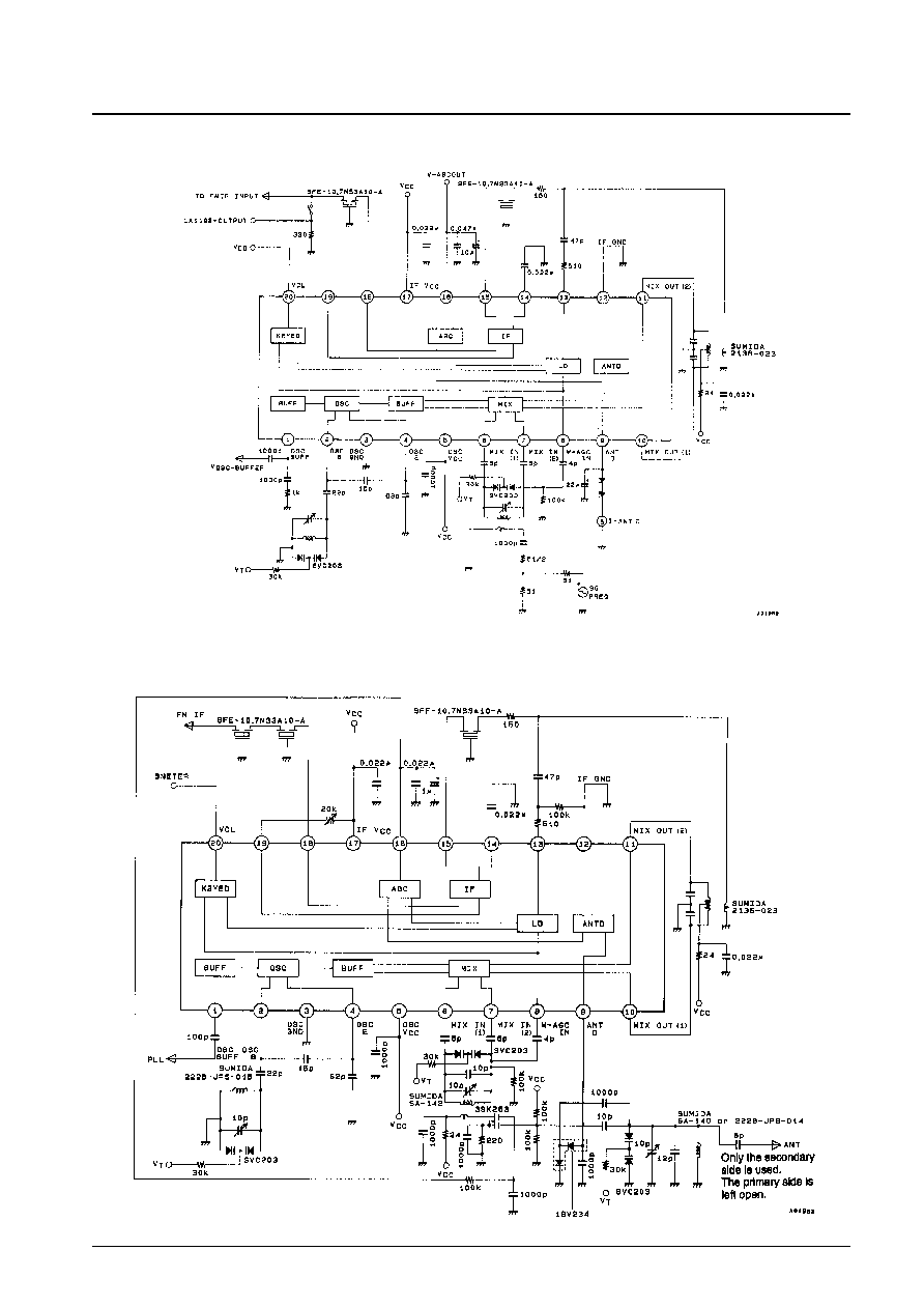
Block Diagram and Test Circuit Diagram
Application Circuit: USA and Europe
No. 4715-3/21
LA1193M, 1193V
Unit (Resistance:
, Capacitance: F)
Unit (Resistance:
, Capacitance: F)

Application Circuit: Japan
Coil Specifications
Coils Manufactured by Sumida Electronics
Japan band RF coil SA-129 or SA-143
Japan oscillator coil SA-125
Japan antenna coil SA-123 or SA-144
US band RF coil SA142 or SA-250
No. 4715-4/21
LA1193M, 1193V
Continued on next page.
Unit (Resistance:
, Capacitance: F)
Continued from preceding page.
US band antenna coil SA-140 or SA-231
US band oscillator coil SA-278
Mixer coil (for both bands) SA-266
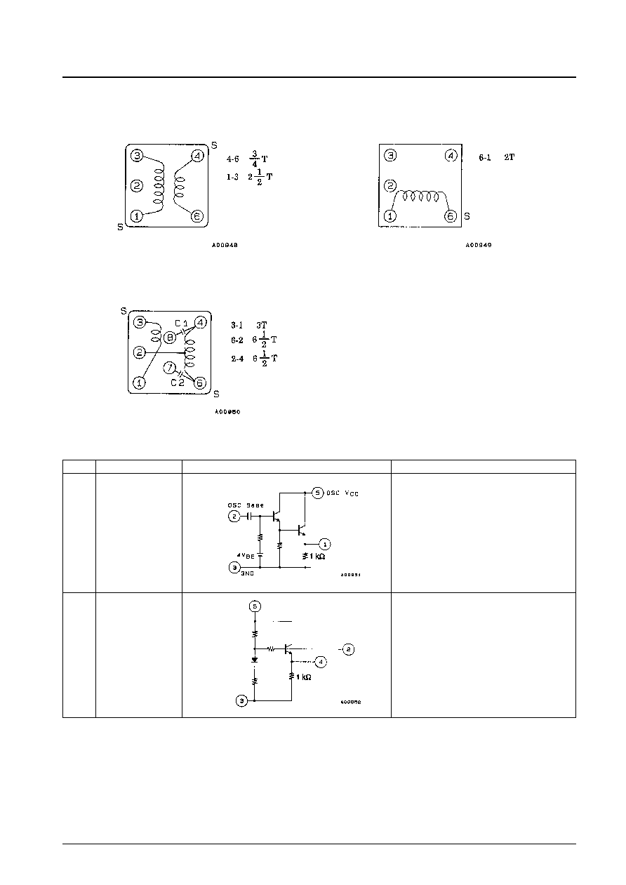
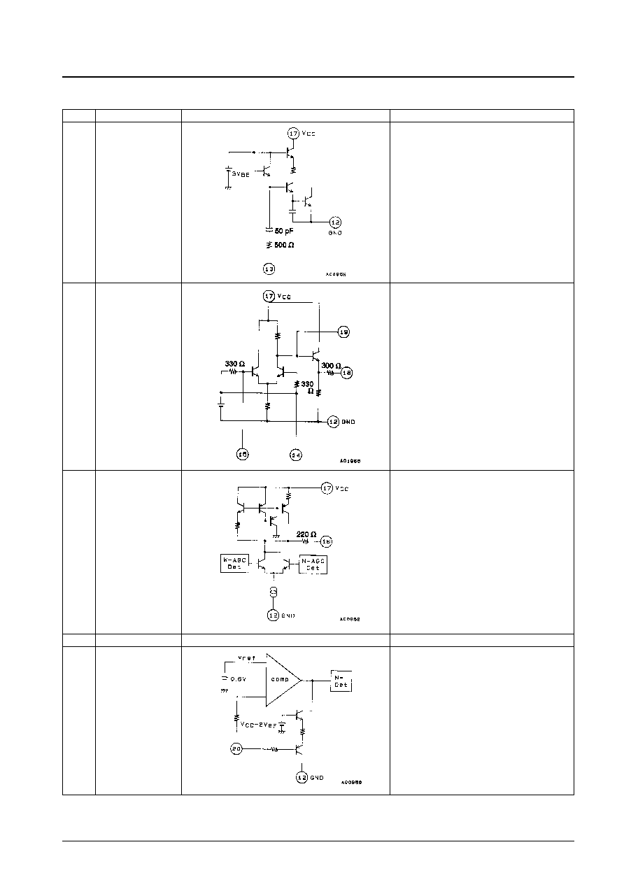
Pin Functions
No. 4715-5/21
LA1193M, 1193V
Pin No.
Function
Equivalent circuit
Note
1
2
3
4
5
OSC BUFF
OSC Tr. base
OSC GND
OSC Tr. emitter
OSC V
CC
Colpitts oscillator
Continued on next page.
Continued from preceding page.
No. 4715-6/21
LA1193M, 1193V
Pin No.
Function
Equivalent circuit
Note
6
7
10
11
9
12
8
Mix input (1)
Mix input (2)
Mix out (1)
Mix out (2)
Antenna damping
drive output
IF GND
W-AGC input
Mixer input usable sensitivity
15 dBÁ
Mixer input I.M. QS
90.5 dBÁ
(6.5 dB higher than previous products)
Conversion gain
15 dB
Input impedance
25
I
ANTD
= 10 mA
Since the DC cut capacitor is provided on-chip in the
pin internal circuit, we have taken steps to prevent
incorrect AGC operation due to inter-pin leakage
currents.
Continued on next page.
Continued from preceding page.
No. 4715-7/21
LA1193M, 1193V
Pin No.
Function
Equivalent circuit
Note
13
14
15
18
19
16
17
20
N-AGC input
IF AMP bypass
IF AMP input
IF AMP output
IF AMP gain adjust
RF AGC output
IF, AGC, V
CC
Keyed AGC input
Since the DC cut capacitor is provided on-chip in the
pin internal circuit, we have taken steps to prevent
incorrect AGC operation due to inter-pin leakage
currents.
IF gain: 25 dB
Input and output impedances of 330
The IF gain can be adjusted by inserting a resistor
between pins 17 and 19.
The gain is at its maximum when there is no resistor
inserted.
MOSFET
Second gate control
Controls the narrow AGC.

1. Oscillator Circuit
Steps were taken to prevent AMR degradation during earlier product type
AGC operation, since the local oscillator block in this IC has independent
Vd (pin 5) and ground (pin 3) connections.
This is a Colpitts oscillator and has the same structure as that used in
earlier circuits. The oscillation level and intensity are changed by
capacitors C
2-4
, C
4
and C
P
.
2. Local Oscillator Buffer Output
This buffer is an emitter follower circuit.
If desired, the buffer efficiency can be increased by inserting a resistor
between pin 1 and ground to pass more current through the buffer
transistor. However, this current must be limited so that Pdmax for the
package is not exceeded.
3. Interference Characteristics
The LA1193M incorporates a newly developed 3D-AGC (triple dimension) circuit. This circuit allows three-signal
interference characteristics (inter-modulation characteristics) and two-signal sensitivity suppression characteristics to
be provided at the same time, a combination of characteristics previously thought difficult to achieve.
Ě Inter-Modulation Characteristics
The LA1193M prevents inter-modulation distortion by applying two wide-band AGC circuits.
No. 4715-8/21
LA1193M, 1193V
Figure 1
This double wide-band AGC system consists of two AGC circuits and a narrow AGC (pin 13 input, mixer input
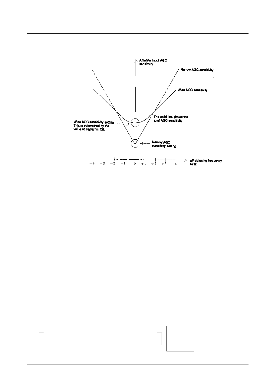
detection type) as shown in Figure 1. Figure 2 shows the antenna input frequency characteristics.
Figure 2 AGC Sensitivity Detuning Characteristics
Features of the Double Wide AGC System
-- Since this is a mixer input detection wide-band AGC, it prevents the occurrence of intermodulation due to
interfering stations with
f > 1 MHz. (TV band interference prevention)
-- Since this system uses a narrow AGC at the same time, the wide AGC sensitivity can be lowered, thus
preventing incorrect operation due to local oscillator injection.
-- Optimal sensitivities for any field conditions can be set, since the sensitivities of both the wide and narrow
AGC systems can be set by changing the values of external components.
-- The input level of the desired station is limited by the narrow AGC. As a result, excessive levels are no longer
input to the stages that follow the mixer and the beats at multiples of 10.7
Î
A are reduced.
Ě Two-Signal Sensitivity Suppression Characteristics
Previously, keyed AGC systems were used to provide good intermodulation distortion and two signal sensitivity
suppression characteristics at the same time. However, in previous keyed AGC systems, when the desired station
would fade or drop out, the wide band AGC level would become essentially zero. As a result, the automatic station
selection function would malfunction and blocking oscillation would occur in the presence of strong interfering
stations. Thus keyed AGC systems were extremely hard to use in actual practice. Sanyo has developed a new AGC
system (3D-AGC) that solves these problems and allows the construction of extremely simple application circuits.
The LA1193M/V incorporates this AGC system.
What is the 3D-AGC system?
It is a system that determines the wide-band AGC level by using information that has the following three frequency
characteristics.
No. 4715-9/21
LA1193M, 1193V
RF and antenna circuit information
Mixer circuit information
C, F and selectivity information
Mixer input AGC
Mixer output AGC
S-meter output
Three
dimensions
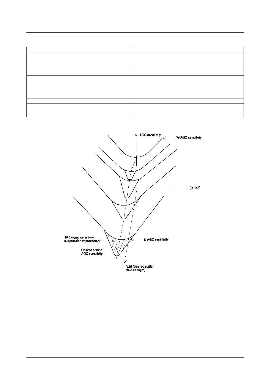
3D-AGC Features
3D-AGC Sensitivity,
f and V20 Characteristics
Figure 3 3D-AGC Sensitivity,
f and V20 Characteristics
-- The W-AGC sensitivity is determined by the antenna RF circuit selectivity independently of V
20
.
-- The N-AGC sensitivity is determined by the antenna, RF and mixer circuit total selectivity when V
20
is 0.6 V
or greater. It is determined by that selectivity and V
20
when V
20
is over 0.6 V.
-- The improvement in two-signal sensitivity suppression is the shaded area in the total AGC sensitivity and
corresponds to the section occupied by the N-AGC.
No. 4715-10/21
LA1193M, 1193V
Feature
Merit
The narrow AGC sensitivity, which operates for
f of less than 1.5 MHz, is
controlled independently according to the field strength of the desired
station.
The narrow AGC sensitivity is controlled at V20 values under 2 V.
The wide AGC operates even when V
20
is zero, i.e., when the desired
station does not exist.
The N-AGC and the W-AGC sensitivities can be set independently.
The system has two AGC systems, the N-AGC and the W-AGC.
Ě This is effective as a measure for mitigating two signal sensitivity
suppression.
Ě This allows two signal sensitivity suppression to be mitigated without
deterioration in the three signal characteristics.
Ě This allows the prevention of incorrect stopping on intermodulation
signals during search.
Ě This allows the prevention of intermodulation occurring in the antenna
and RF modulation circuits in the presence of strong interfering stations.
Prevention of blocking oscillation due to AGC operation is also possible.
Ě This allows optimal settings to match the reception field conditions.
Ě Since the narrow AGC operates at the desired station and at adjacent
stations, it is possible to reduce the wide AGC sensitivity. This prevents
incorrect AGC operation due to local oscillator injection.

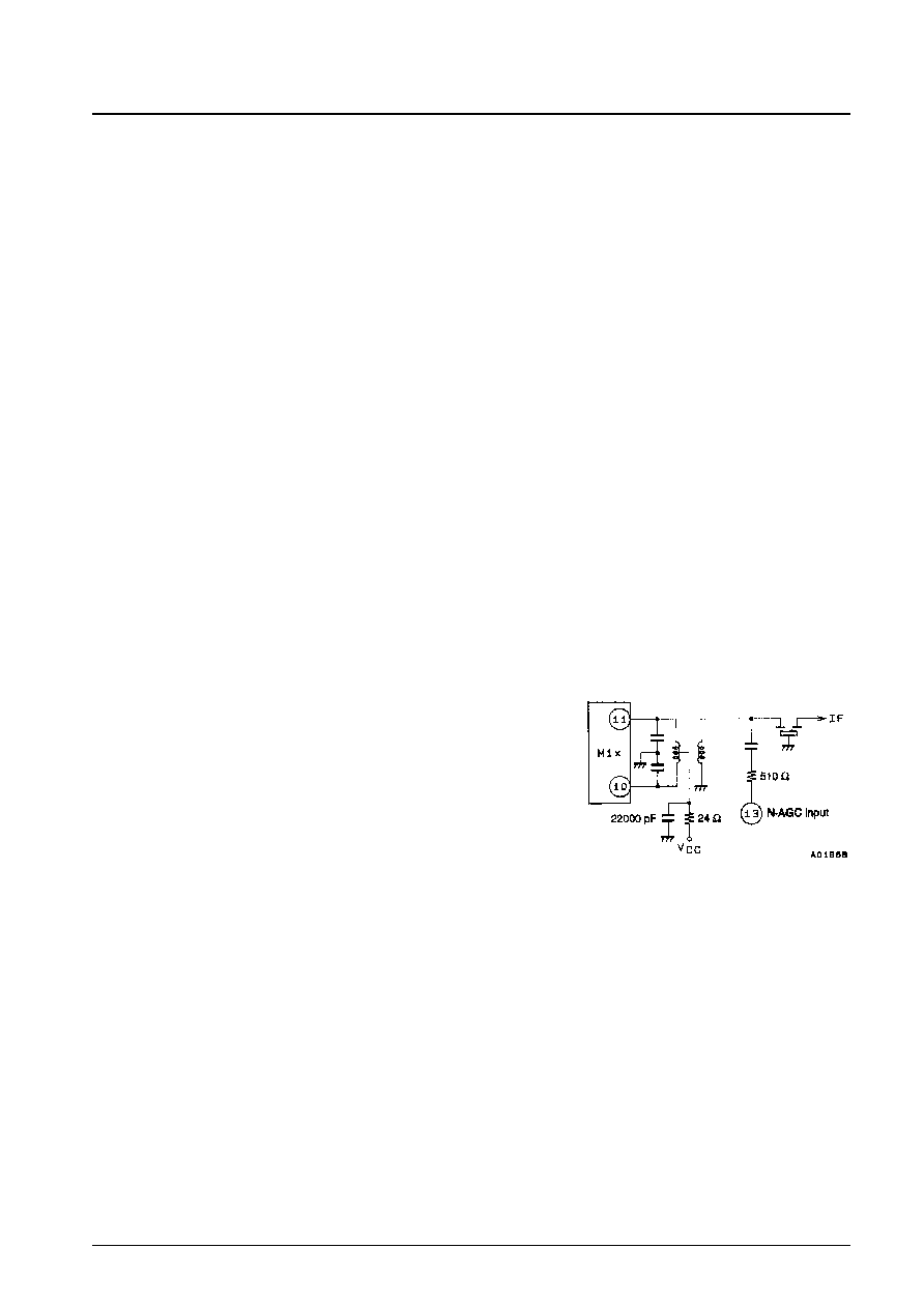
4. Mixer
The mixer circuit used in this IC is a balanced input/balanced output double balance mixer circuit.
Ě Input Format
Emitter input
Input impedance: 25
Optimization of the component geometry, emitter
current and bias allow this circuit to achieve the
following performance.
Mixer input usable sensitivity: 15 dBÁ
Mixer input IMQS*: 90.5 dBÁ
Note: * Mixer input IMQS is defined as follows:
5. IF Amplifier
This IF amplifier is a single stage differential amplifier.
Specifications
Input impedance:
330
Output impedance: 330
Gain:
25 dB
Gain adjustment can be provided using either of
the methods shown.
Temperature Characteristics
The LA1193M/V uses Vref temperature characteristics correction to hold the gain temperature characteristics to the
low level of about 1 dB over the range ş30 to +80░C.
No. 4715-11/21
LA1193M, 1193V
fr = 98.8 MHz, no input
fu1 = 98.8 MHz, 1 kHz, 30% modulation
fu2 = 99.6 MHz, no modulation
IMQS is the interference 1 and 2 input levels such that when an
interference signal with the same level is input to the mixer and
distortion occurs at the mixer, the generated IM output has a S/N
ratio of 30 dB.
Figure 4 Mixer Circuit
(Improved by 6.0 dBÁ over previous products.)
IF Gain adj
6. AGC Circuit
The LA1193M/V uses pin diode antenna damping (pin 9) and MOSFET second gate voltage control (pin 16) for
AGC. The AGC operating sequence is as follows:
Antenna damping (pin diode)
MOSFET second gate voltage control
(attenuation) 20 dB
(attenuation) dB
The above AGC sequence is used for the following reasons.
Ě Intermodulation distortion can occur if a signal of 110 dBÁ or larger is input to the antenna circuit varactor diode.
In such situations, if the AGC sequence was MOSFET second gate voltage control followed by pin diode antenna
damping, as long as the receiver was not in a strong field where the 60 dB or higher AGC attenuation operates,
input limitation due to the antenna circuit varactor diode would operate. Therefore, we feel that the AGC operating
sequence employed is appropriate.
Ě Consider the problem of AGC loop stability. If the two AGC loops (the antenna damping AGC loop and the
MOSFET second gate control AGC loop) operate, the AGC system would become unstable and have an
excessively large influence on the transient response. Therefore the following structure cannot be used.
MOSFET second gate control
antenna damping
MOSFET second gate control
The AGC operating conditions are the same as those for the LA1175M.
Ě Narrow AGC circuit
Since the LA1193M/V's N-AGC (which detects the mixer output) is set to have a high sensitivity, care is required
to avoid incorrect operation. In particular, there must be adequate separation from the local oscillator block on the
printed circuit board pattern. Also, a resistor of at least 500
must be inserted at the pin 13 input. A low-pass filter
is formed by the insertion of this resistor. This low-pass filter prevents incorrect AGC operation due to the local
oscillator.
Ě The AGC sensitivity setting can be changed by adjusting the
value of the capacitor connected at pin 13. Although the AGC
sensitivity can be lowered by increasing the value of the series
resistor, caution is required since the AGC has its own frequency
characteristics.
Ě Wide AGC circuit
The wide AGC sensitivity is set by the value of the capacitor on pin 8. However, since incorrect operation due to
the local oscillator signal may occur if this capacitor is too large, its value must be chosen carefully.
Ě 3D-AGC
If the difference in sensitivity between the N-AGC and the W-AGC systems is too large during 3D-AGC
operation, the S/N ratio can be degraded in the vicinity of the input where the AGC switches. Therefore, the
3D-AGC setting values must be selected carefully. Although this problem can be ameliorated by applying a time
constant to pin 20, in principle, this S/N ratio degradation should be prevented by limiting the sensitivity difference
between the two AGC systems.
No. 4715-12/21
LA1193M, 1193V
No. 4715-13/21
LA1193M
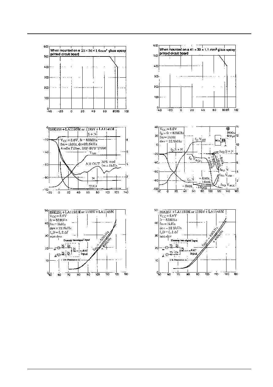
Pd max ş Ta [LA1193M]
Allowable power dissipation, Pdmax ş mW
Ambient temperature, Ta ş ░C
Pd max ş Ta [LA1193M]
Allowable power dissipation, Pdmax ş mW
Ambient temperature, Ta ş ░C
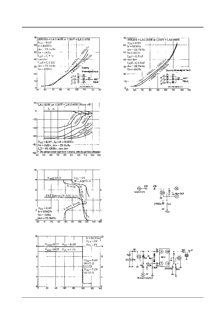
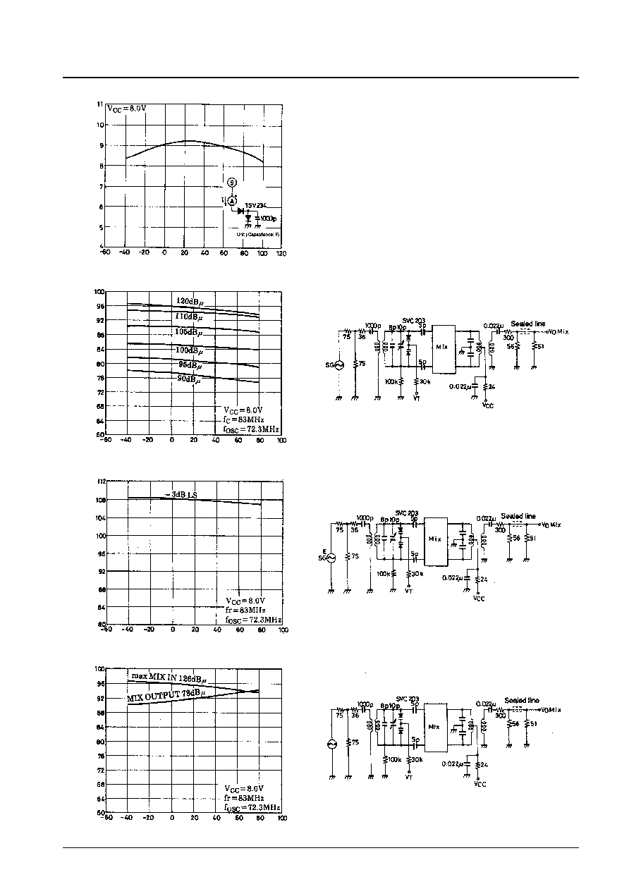
I/O characteristics
Noise, AF out ş dBm
Antenna input level ş dBÁ
Two-signal interference characteristics
Desired station input level ş dB
Á
Interfering station input level ş dBÁ
I/O characteristics
S-meter voltage, V
SM
ş V
Total harmonic distortion, THD ş %
AF out, noise out, AM out şdBm
AGC output voltage, V
AGC
ş V
S-meter voltage, V
SM
ş V
Total harmonic distortion, THD ş %
Antenna input level ş dBÁ
Two-signal interference characteristics
Desired station input level ş dB
Á
Interfering station input level ş dBÁ
No. 4715-14/21
LA1193M, 1193V
Three-signal interference characteristics
Desired station input level ş dB
Á
Interfering station input level ş dBÁ
Three-signal interference characteristics
Desired station input level ş dB
Á
Interfering station input level ş dBÁ
Two-signal interference characteristics
Noise, AF out ş dBm
Interference antenna input ş dBÁ
Unit (Resistance:
, Capacitance: F)
V
O AGC
, I
ANT-D
ş V
IN
MIX
AGC output voltage, V
AGC
ş V
Antenna damping current ş mA
Mixer input ş dBÁ
V
O AGC
, antenna dump, FET source ş V
IN
ANT
Pin 16 AGC output voltage ş V
Antenna damping voltage (pin 9), FET source ş V
Antenna input ş dBÁ
Unit (Resistance:
, Capacitance: F)

No. 4715-15/21
LA1193M, 1193V
V
O AGC
, I
ANT-D
ş V
IN AGC
Pin 16 AGC output voltage, ş V
Antenna damping current ş mA
Pin 13 AGC input ş dBÁ (the input value at point A)
V
O AGC
, I
ANT-D
ş V
IN AGC
Pin 16 AGC output voltage ş V
Antenna damping current ş mA
Pin 8 AGC input ş dBÁ (the input value at point A)
V
O AGC
, I
ANT-D
ş V
IN
MIX
AGC output voltage,V
AGC
ş V
Antenna damping current ş mA
Mixer input ş dBÁ
Unit (Resistance:
, Capacitance: F)
AGC frequency response
AGC input level ş dB
Á
(Pin 16 V
AGC
:
2 V)
AGC input frequency ş MHz
AGC frequency response
AGC input level ş dB
Á
(Pin 16 V
AGC
:
2 V)
AGC input frequency ş MHz
Mixer input ş
f
f ş MHz
Unit (Resistance:
, Capacitance: F)

No. 4715-16/21
LA1193M, 1193V
AGC ON levelş Ta
Pin 20 voltage, V
CL
ş V
Ambient temperature, Ta ş ░C
AGC ON level ş Ta
AGC ON level ş dB
Á
Ambient temperature, Ta ş ░C
V
AGC
ş V
CL20
AGC input ON level ş dB
Á
(AGC ş ON =
V
AGC
< 2 V, pin 13 input)
Pin 20 voltage, V
CL20
ş V
V
AGC20
ş V
CL20
N-AGC ON level
(V16 < 2 V) (N-AGC pin 13 input)
Pin 20 voltage, V
CL
ş V
V
AGC
ş f
V
AGC
-ON level ş dB
Á
(when pin 16
>
2 V)
AGC input frequency ş MHz
AGC ON level ş Ta
AGC ON level ş dB
Á
(when pin 16
2 V)
Ambient temperature, Ta ş ░C
Unit (Resistance:
, Capacitance: F)
No. 4715-17/21
LA1193M, 1193V
I
ANT-D
ş V
CL
Antenna damping current ş mA
Pin 20 voltage, V
CL
ş V
V
AGC OUT
ş V
CL
Pin 16 AGC output voltage ş V
Pin 20 voltage, V
CL
ş V
Unit (Resistance:
, Capacitance: F)
V
OIF
ş V
IN IF
IF output ş dB
Á
IF input voltage ş dBÁ
V
O
MIX ş V
IN
MIX
Mixer output ş dB
Á
Mixer input ş dBÁ
Unit (Resistance:
, Capacitance: F)
Unit (Resistance:
, Capacitance: F)
No. 4715-18/21
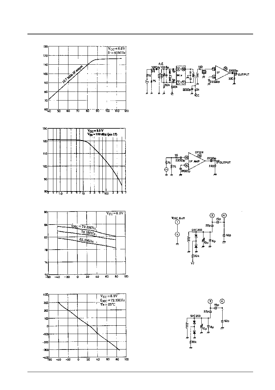
LA1193M, 1193V
IF AMP ş f
Pin 18 IF output ş dB
Á
IF input frequency ş MHz
V
O
IF ş Ta
Pin 18 IF output ş dB
Á
IF input voltage ş dBÁ
f
OSC
ş Ta
Pin 1 oscillator buffer output,
f
OSC
ş MHz
Ambient temperature, Ta ş ░C
V
OSC
ş Ta
Oscillator buffer output voltage ş dB
Á
Ambient temperature, Ta ş ░C
Unit (Resistance:
, Capacitance: F)
Unit (Resistance:
, Capacitance: F)
Unit (Resistance:
, Capacitance: F)
Unit (Resistance:
, Capacitance: F)

No. 4715-19/21
LA1193M, 1193V
V
IN IF
ş Ta
IF input level ş dB
Á
Ambient temperature, Ta ş ░C
V
OIF
ş Ta
IF output level ş dB
Á
Ambient temperature, Ta ş ░C
Unit (Resistance:
, Capacitance: F)
Unit (Resistance:
, Capacitance: F)
MIX ş Ta
Mixer input level ş dB
Á
Ambient temperature, Ta ş ░C
V
O
IF ş Ta
IF output level ş dB
Á
Ambient temperature, Ta ş ░C
Unit (Resistance:
, Capacitance: F)
Unit (Resistance:
, Capacitance: F)
No. 4715-20/21
LA1193M, 1193V
V
O
MIX ş Ta
V
O
MIX ş dB
Á
Ambient temperature, Ta ş ░C
I
ANT-D
ş Ta
Antenna damping current ş mA
Ambient temperature, Ta ş ░C
V
IN
MIX ş Ta
V
IN
MIX ş dB
Á
Ambient temperature, Ta ş ░C
V
IN
MIX ş Ta
V
IN
MIX ş dB
Á
Ambient temperature, Ta ş ░C
Unit (Resistance:
, Capacitance: F)
Unit (Resistance:
, Capacitance: F)
Unit (Resistance:
, Capacitance: F)

No. 4715-21/21
LA1193M, 1193V
V
OSC
ş V
CC
Oscillator buffer output level ş dB
Á
Supply voltage, V
CC
ş V
V
OSC
ş R
L
Oscillator buffer output ş dB
Á
Load resistance, R
L
ş
f
OSC
ş V
CC
f
OSC
ş kHz
Supply voltage, V
CC
ş V
Unit (Resistance:
, Capacitance: F)
Unit (Resistance:
, Capacitance: F)
Unit (Resistance:
, Capacitance: F)
This catalog provides information as of March, 1997. Specifications and information herein are subject to
change without notice.
s
No products described or contained herein are intended for use in surgical implants, life-support systems, aerospace
equipment, nuclear power control systems, vehicles, disaster/crime-prevention equipment and the like, the failure of
which may directly or indirectly cause injury, death or property loss.
s
Anyone purchasing any products described or contained herein for an above-mentioned use shall:
Accept full responsibility and indemnify and defend SANYO ELECTRIC CO., LTD., its affiliates, subsidiaries and
distributors and all their officers and employees, jointly and severally, against any and all claims and litigation and all
damages, cost and expenses associated with such use:
Not impose any responsibility for any fault or negligence which may be cited in any such claim or litigation on
SANYO ELECTRIC CO., LTD., its affiliates, subsidiaries and distributors or any of their officers and employees
jointly or severally.
s
Information (including circuit diagrams and circuit parameters) herein is for example only; it is not guaranteed for
volume production. SANYO believes information herein is accurate and reliable, but no guarantees are made or implied
regarding its use or any infringements of intellectual property rights or other rights of third parties.