2SK3101LS
No.7910-1/5
Features
·
Low ON-resistance.
·
Low Qg.
·
Ultrahigh-Speed Switching Applications.
·
Avalanche resistance guarantee.
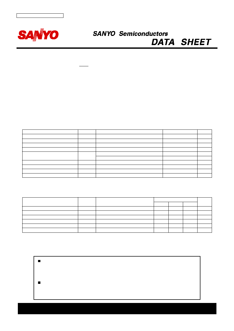
Specifications
Absolute Maximum Ratings
at Ta=25
°
C
Parameter
Symbol
Conditions
Ratings
Unit
Drain-to-Source Voltage
VDSS
400
V
Gate-to-Source Voltage
VGSS
±
30
V
Drain Current (DC)
ID
11
A
Drain Current (Pulse)
IDP
PW
10
µ
s, duty cycle
1%
44
A
Allowable Power Dissipation
PD
2.0
W
Tc=25
°
C
40
W
Channel Temperature
Tch
150
°
C
Storage Temperature
Tstg
--55 to +150
°
C
Avalanche Enargy (Single Pulse) *1
EAS
69.1
mJ
Avalanche Current *2
IAV
11
A
*1 VDD=50V, L=1mH, IAV=11A
*2 L
1mH, single pulse
Electrical Characteristics
at Ta=25
°
C
Ratings
Parameter
Symbol
Conditions
min
typ
max
Unit
Drain-to-Source Breakdown Voltage
V(BR)DSS
ID=1mA, VGS=0
400
V
Zero-Gate Voltage Drain Current
IDSS
VDS=320V, VGS=0
1.0
m
A
Gate-to-Source Leakage Current
IGSS
VGS=
±
30V, VDS=0
±
100
n
A
Cutoff Voltage
VGS(off)
VDS=10V, ID=1mA
3.0
4.0
V
Forward Transfer Admittance
yfs
VDS=10V, ID=8A
4.0
8.0
S
Static Drain-to-Source On-State Resistance
RDS(on)
ID=8A, VGS=15V
0.32
0.4
Marking : K3101
Continued on next page.
SANYO Electric Co.,Ltd. Semiconductor Company
TOKYO OFFICE Tokyo Bldg., 1-10, 1 Chome, Ueno, Taito-ku, TOKYO, 110-8534 JAPAN
Ordering number : ENN7910
Any and all SANYO products described or contained herein do not have specifications that can handle
applications that require extremely high levels of reliability, such as life-support systems, aircraft's
control systems, or other applications whose failure can be reasonably expected to result in serious
physical and/or material damage. Consult with your SANYO representative nearest you before using
any SANYO products described or contained herein in such applications.
SANYO assumes no responsibility for equipment failures that result from using products at values that
exceed, even momentarily, rated values (such as maximum ratings, operating condition ranges, or other
parameters) listed in products specifications of any and all SANYO products described or contained
herein.
81004 TS IM TB-00000033
2SK3101LS
N-Channel Silicon MOSFET
General-Purpose Switching Device
Applications
2SK3101LS
No.7910-2/5
Continued from preceding page.
Ratings
Parameter
Symbol
Conditions
min
typ
max
Unit
Input Capacitance
Ciss
VDS=20V, f=1MHz
1850
pF
Output Capacitance
Coss
VDS=20V, f=1MHz
480
pF
Reverse Transfer Capacitance
Crss
VDS=20V, f=1MHz
240
pF
Turn-ON Delay Time
td(on)
See specified Test Circuit.
19
ns
Rise Time
tr
See specified Test Circuit.
35
ns
Turn-OFF Delay Time
td(off)
See specified Test Circuit.
140
ns
Fall Time
tf
See specified Test Circuit.
41
ns
Total Gate Charge
Qg
VDS=200V, VGS=10V, ID=11A
58
nC
Diode Forward Voltage
VSD
IS=11A, VGS=0
0.9
1.2
V
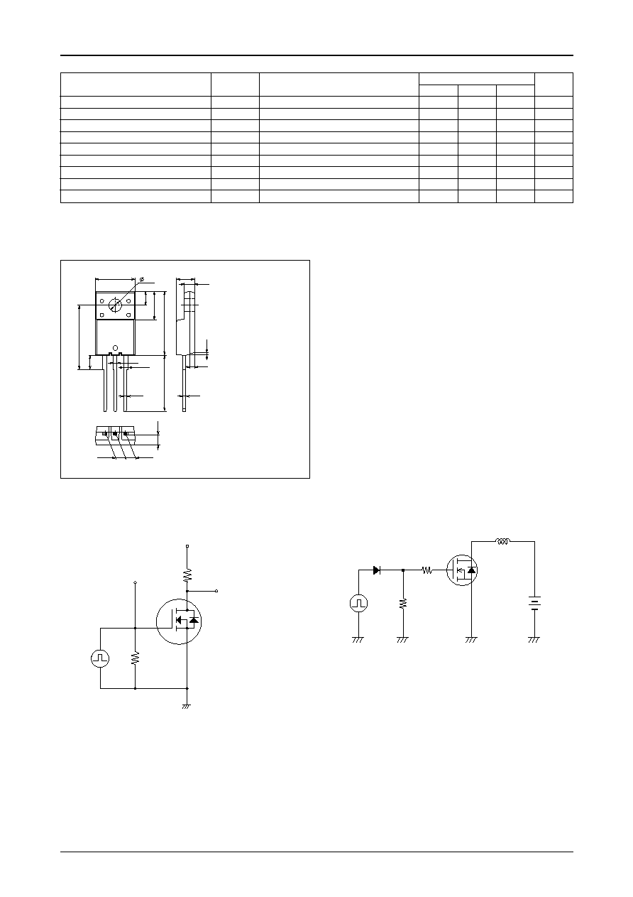
Package Dimensions
unit : mm
2078C
Switching Time Test Circuit
Unclamped Inductive Test Circuit
1 : Gate
2 : Drain
3 : Source
SANYO : TO-220FI(LS)
16.0
14.0
3.6
3.5
7.2
16.1
0.7
2.55
2.55
2.4
1.2
0.9
0.75
0.6
1.2
4.5
2.8
1 2 3
10.0
3.2
PW=1
µ
s
P.G
RGS
50
G
S
D
ID=8A
RL=25
VDD=200V
VGS=15V
VOUT
2SK3101LS
D.C.
0.5%
50
50
DUT
VDD
L
10V
0V
2SK3101LS
No.7910-3/5
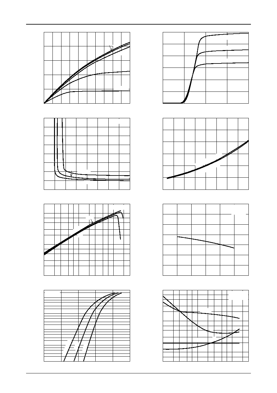
0
20
15
10
5
30
25
20
15
10
5
0
--50
150
125
100
75
50
25
0
--25
Gate-to-Source Voltage, VGS -- V
RDS(on) -- VGS
IT06563
25
20
15
10
5
0
0.2
10
9
8
7
6
5
4
3
2
1
Drain-to-Source Voltage, VDS -- V
ID -- VDS
Drain Current, I
D
-
-
A
IT06561
Gate-to-Source Voltage, VGS -- V
ID -- VGS
Drain Current, I
D
-
-
A
VDS=10V
IT06562
Case Temperature, Tc --
°
C
RDS(on) -- Tc
IT06564
4
6
8
10
12
14
16
18
20
1.0
0.9
0.8
0.7
0.6
0.5
0.4
0.3
0
VGS=6V
7V
8V
10V
15V
25
°
C
75
°
C
ID=16A
1A
8A
Tc=25
°
C
I D
=8A, V
GS
=10V
I D
=8A, V
GS
=15V
Static Drain-to-Source
On-State Resistance, R
DS
(on) -
-
Static Drain-to-Source
On-State Resistance, R
DS
(on) -
-
Tc= --25
°
C
0.2
0.4
0.6
0.8
1.0
1.2
0
1.2
1.0
0.8
0.6
0.4
0.2
Diode Forward Voltage, VSD -- V
IF -- VSD
Forward Current, I
F
-
-
A
IT06567
Drain Current, ID -- A
IT06565
2
7
5
3
2
7
5
3
2
3
10
1.0
0.1
0.1
1.0
10
2
3
5
7
2
3
5
7
2
0.001
7
5
3
2
7
5
3
2
3
2
10
1.0
0.1
0.01
3
2
7
5
3
2
5
7
Forward T
ransfer
Admittance,
yfs
-
-
S
y
fs
-- ID
IT06566
200
150
100
50
0
--50
--100
0
7
6
5
4
3
2
1
Case Temperature, Tc --
°
C
Cutof
f V
oltage,
V
GS
(of
f)
--
V
VGS(off) -- Tc
VDS=10V
25
°
C
75
°
C
VGS=
0
V
--25
°
C
25
°
C
Tc= -
-25
°
C
VDS=10V
ID=1mA
Tc
=
75
°
C
Drain Current, ID -- A
Switching
T
ime, SW
T
ime -
-
ns
SW Time -- ID
IT07364
10
100
1000
5
7
3
2
5
7
3
2
5
7
0.1
1.0
2
3
5
7
2
3
5
7
2
3
10
VDD=200V
VGS=15V
td(off)
tr
td(on)
tf
2SK3101LS
No.7910-4/5
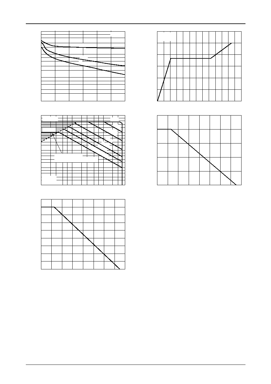
100
10
1.0
2
3
5
7
2
3
5
7
5
2
3
65
60
55
50
45
40
35
30
25
20
15
10
5
0
0
12
10
8
6
4
2
Total Gate Charge, Qg -- nC
VGS -- Qg
Gate-to-Source V
oltage, V
GS
-
-
V
IT06569
0
0
0
20
40
45
2.5
2.0
1.5
1.0
0.5
40
35
30
25
20
15
10
5
60
80
100
120
140
160
160
140
120
100
80
60
40
20
0
Case Temperature, Tc --
°
C
Ambient Temperature, Ta --
°
C
PD -- Tc
PD -- Ta
Allowable Power Dissipation, P
D
--
W
Allowable Power Dissipation, P
D
--
W
IT06571
IT06572
A S O
Drain-to-Source Voltage, VDS -- V
Drain Current, I
D
--
A
IT06570
Ciss, Coss, Crss -- VDS
Drain-to-Source Voltage, VDS -- V
Ciss, Coss, Crss -
-
pF
IT06568
0.01
0.1
1.0
10
100
2
3
5
7
2
3
3
5
2
3
5
7
2
3
5
7
Crss
Coss
Ciss
f=1MHz
VDS=
200
V
ID=
11
A
ID=11A
<
1
µ
s
IDP=44A
Operation in this
area is limited by RDS(on).
Tc=25
°
C
Single pulse
0
5
10
15
20
25
30
10
100
1000
10000
5
7
2
3
7
3
5
5
7
2
2
3
DC operation
100ms
10ms
1ms
10
µ
s
100
µ
s
2SK3101LS
No.7910-5/5
PS
Specifications of any and all SANYO products described or contained herein stipulate the performance,
characteristics, and functions of the described products in the independent state, and are not guarantees
of the performance, characteristics, and functions of the described products as mounted in the customer's
products or equipment. To verify symptoms and states that cannot be evaluated in an independent device,
the customer should always evaluate and test devices mounted in the customer's products or equipment.
SANYO Electric Co., Ltd. strives to supply high-quality high-reliability products. However, any and all
semiconductor products fail with some probability. It is possible that these probabilistic failures could
give rise to accidents or events that could endanger human lives, that could give rise to smoke or fire,
or that could cause damage to other property. When designing equipment, adopt safety measures so
that these kinds of accidents or events cannot occur. Such measures include but are not limited to protective
circuits and error prevention circuits for safe design, redundant design, and structural design.
In the event that any or all SANYO products(including technical data,services) described or
contained herein are controlled under any of applicable local export control laws and regulations,
such products must not be exported without obtaining the export license from the authorities
concerned in accordance with the above law.
No part of this publication may be reproduced or transmitted in any form or by any means, electronic or
mechanical, including photocopying and recording, or any information storage or retrieval system,
or otherwise, without the prior written permission of SANYO Electric Co. , Ltd.
Any and all information described or contained herein are subject to change without notice due to
product/technology improvement, etc. When designing equipment, refer to the "Delivery Specification"
for the SANYO product that you intend to use.
Information (including circuit diagrams and circuit parameters) herein is for example only ; it is not
guaranteed for volume production. SANYO believes information herein is accurate and reliable, but
no guarantees are made or implied regarding its use or any infringements of intellectual property rights
or other rights of third parties.
This catalog provides information as of August, 2004. Specifications and information herein are subject
to change without notice.
Note on usage : Be careful in handling the 2SK3101LS because it has no protection diode
between gate and source.