
s Features
q
Repetitive peak off-state voltage: V
DRM
=200, 400, 600V
q
Average on-state current: I
T(AV)
=3A
q
High sensitive Gate trigger Current: I
GT
=0.1mA max
sAbsolute Maximum Ratings
sElectrical Characteristics
Parameter
Symbol
Ratings
Unit
Conditions
V
Tj= 40 to +125
°
C, R
GK
=1k
50Hz Half-cycle sinewave, Continuous current, Tc =87
°
C
50Hz Half-cycle sinewave, Single shot, Non-repetitive, Tj=125
°
C
200
TF321M-A TF341M-A TF361M-A
600
200
600
300
700
300
700
400
V
V
V
A
A
A
A
V
V
W
W
°
C
°
C
V
DRM
V
RRM
V
DSM
V
RSM
I
T(AV)
I
T(RMS)
I
TSM
I
FGM
V
FGM
V
RGM
P
GM
P
G (AV)
Tj
Tstg
400
500
500
3.0
4.7
60
2.0
10
5.0
5.0
0.5
40 to +125
40 to +110
V
V
mA
V
mA
V/
µ
S
µ
S
°
C/W
Parameter
Symbol
Ratings
typ
min
max
Unit
Conditions
mA
mA
I
DRM
V
TM
I
GT
tq
I
RRM
V
GT
V
GD
I
H
dv/dt
Rth
1.0
20
30
3.0
0.1
1.4
1
0.1
1.0
1.0
Tj=125
°
C,
V
D
=V
DRM
(V
RRM
), R
GK
=1k
T
C
=25
°
C,
I
TM
=5A
V
D
=6V, R
L
=10
, T
C
=25
°
C
R
GK
=1k
, Tj=25
°
C
Junction to case
Tc= 25
°
C
V
D
=1/2
×
V
DRM
, Tj=125
°
C,
R
GK
=1k
, C
GK
=0.033
µ
F
V
D
=1/2
×
V
DRM
, Tj=125
°
C,
R
GK
=1k
18
TF321M-A, TF341M-A, TF361M-A
TO-220 3A High sensitive Thyristor
1.7
±
0.2
3.0
±
0.2
8.8
±
0.2
3.75
±
0.1
1.35
±
0.15
2.5
±
0.1
2.5
±
0.1
+
0.2
0.1
0.65
10.4max
16.7max
5.0max
2.1max
12.0
min
4.0
max
Weight: Approx. 2.6g
External Dimensions
(Unit: mm)
(1). Cathode (K)
(2). Anode (A)
(3). Gate (G)
(1) (2) (3)
a. Part Number
b. Lot Number
a
b
Repetitive peak off-state voltage
Repetitive peak reverse voltage
Non-repetitive peak off-state voltage
Non-repetitive peak reverse voltage
Average on-state current
RMS on-state current
Surge on-state current
Peak forward gate current
Peak forward gate voltage
Peak reverse gate voltage
Peak gate power loss
Average gate power loss
Junction temperature
Storage temperature
Off-state current
Reverse current
On-state voltage
Gate trigger voltage
Gate trigger current
Gate non-trigger voltage
Holding current
Critical rate-of-rise of off-state voltage
Turn-off time
Thermal resistance
f 50Hz
f 50Hz, duty 10%
f 50Hz, duty 10%
0.3
0.5
1
100
50
10
5
1.0
2.0
4.0
3.0
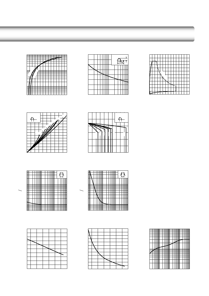
On-state voltage
v
T
( V )
On-state current
i
T
(A)
v
T
i
T
Characteristics (max)
Tj=125
°
C
Tj=25
°
C
0
20
40
60
80
Number of cycle
Surge on-state current I
TSM
(A)
I
TSM
Ratings
1
5
10
50
100
0
1
3
2
0
2
4
6
8
12
10
Gate Characteristics
1 cycle
10 ms
TSM
I
0
0
1
2
3
4
5
7
6
1
3
4
2
5
Average on-state current I
T(AV)
(A)
I
T(AV )
P
T(AV)
Characteristics
60
°
90
°
120
°
150
°
180
°
DC
=30
°
0
0
25
50
100
75
150
125
5
4
3
1
2
Average on-state current I
T(AV)
(A)
I
T(AV)
Tc Ratings
60
°
90
°
150
°
120
°
180
°
DC
=3
0
°
40
0
75
125
100
25
50
0.8
1.0
0.6
0.4
0
0.2
0
10
20
24
40
0
75
125
100
25
50
1
10
10
2
10
3
0.5
1
5
50
10
1
10
10
2
10
3
0.5
1
5
50
10
1
10
10
2
10
3
10
4
0.1
1
10
Average on-state power P
T
( AV
)
(W
)
Case temperature T
C
(
°
C)
19
(V
D
=6V, R
L
=10
)
(V
D
=6V, R
L
=10
)
Gate current
i
GF
(A)
Gate voltage
v
GF
(V)
P
GM
=5
W
TF321M-A, TF341M-A, TF361M-A
Tj=125
°
C
Initial junction temperature
50Hz Half-cycle sinewave
: Conduction angle
180
°
0
°
50Hz Half-cycle sinewave
: Conduction angle
180
°
0
°
Pulse width
t
w (
µ
s)
Pulse trigger temperature
Characteristics
v
gt
(Typical)
v
gt
V
GT
DC gate trigger
voltage at 25
°
C
( )
( )
Gate trigger voltage
at Ta and
t
w
v
gt
50%
t
w
Pulse width
t
w (
µ
s)
Pulse trigger temperature
Characteristics
i
gt
(Typical)
i
gt
I
GT
DC gate trigger
current at 25
°
C
( )
( )
Gate trigger current
at Ta and
t
w
i
gt
t
w
50%
Junction temperature Tj (
°
C)
Gate trigger voltage V
GT
(V)
V
GT
temperature Characteristics
(Typical)
Junction temperature Tj (
°
C)
Gate trigger current I
GT
(
µ
A)
I
GT
temperature Characteristics
(Typical)
t, Time (ms)
Transient thermal resistance
r
th
(
°
C/
W
)
Transient thermal resistance
Characteristics
(Junction to case)