Parameter
Symbol
Unit
Conditions
Ratings
Absolute Maximum Ratings
(Ta=25¤C)
Power supply voltage
Power Dissipation
Storage temperature
Channel temperature
Output avalanche capability
V
B
P
D
Tstg
Tch
E
AV
V
W
¤C
¤C
mJ
Single pulse
40
Input terminal voltage
V
( IN, SEL, B/U)
V
Ù0.5 to +6.5
Output terminal voltage (DC)
V
OUT
V
50
Output terminal voltage (pulse)
V
OUT
V
Output clamping (max 70V)
Output current (DC)
I
OUT
A
Ý
2.9
Output current (pulse)
I
OUT
A
Over current protection starting current
Diag output source current
V
DIAG
V
6.5
Diag output voltage
I
DIAG
mA
5
2.8
Ù40 to +150
150
80
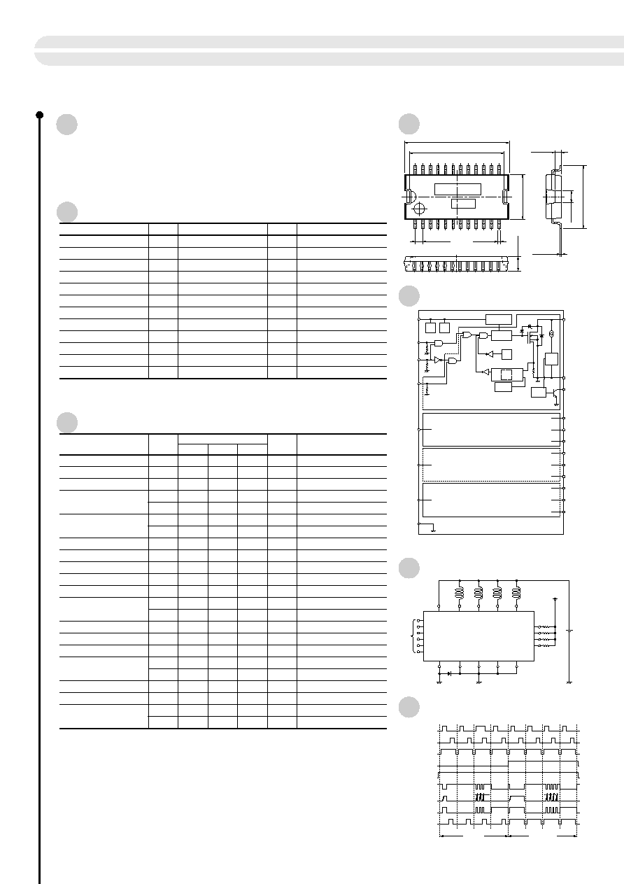
Equivalent Circuit Diagram
Circuit Example
Timing Chart
External Dimensions
(unit: mm)
Features
q DMOS 4ch output
q Allows ON/OFF using C-MOS logic level
q Built-in over current and thermal protection circuit and diagnostic function to
detect open load
q Built-in output status signals (over current, over heat and open load)
42
V
B
(7)
V
IN
B/U
(17)
V
IN
SEL
(5)
V
IN
1
(6)
V
IN
2
(8)
V
IN
3
(18)
V
IN
4
(20)
L-GND
(19)
V
OUT
1
(4)
V
OUT
2
(9)
V
DIAG
1
(3)
V
OUT
SENSE
V
DIAG
2
(10)
P-GND1
(1, 2)
P-GND2
(11, 12)
V
OUT
3
(16)
V
DIAG
3
(15)
P-GND3
(13, 14)
V
OUT
4
(21)
V
DIAG
4
(22)
P-GND4
(23, 24)
Reg
Ref
Gate Protection
Gate driver
TSD
OUT OCP
Latch
Set
Reset
OSC
Monitor
V
B
7
6
3
10
15
22
8
18
20
17
19
1, 2
11, 12
13, 14
23, 24
5
4
9
16
21
LG
PG1
PG2
PG3
PG4
V
IN
1
V
IN
2
V
IN
3
V
IN
4
V
IN
B/U
V
IN
SEL
OUT1
OUT2
OUT3
OUT4
DIAG1
DIAG2
DIAG3
DIAG4
SPF5009
Main input signal 1
V
IN
1
Main input signal 2
V
IN
2
Backup input signal
V
IN
B/U
Input select signal
V
IN
SEL
Power supply voltage
V
B
Output voltage 1
V
OUT
1
Output current 1
I
OUT
1
DIAG output 1
V
DIAG
1
DIAG output 2
V
DIAG
2
Nomal
Nomal
Main mode
Backup mode
Output 1
Overheat
Output 1
Overheat
Output 1
Over current
Output 1
Open load
Output 1
Over current
Output 1
Open load
OCP
OCP
Electrical Characteristics
Parameter
Symbol
min
typ
max
Unit
Conditions
Ratings
Quiescent circuit current
Operating circuit current
Overcurrent protection starting current
Forward voltage of output stage diode
Output moniter threshold voltage
(V
B
=14V, Ta
= 25¤C unless otherwise specified)
I
q
V
B
=14V, V
IN
=0V
V
B
=14V, V
O
=1A
V
B
=14V
V
B
=14V, R
L
=14
, I
O
=1A
V
B
=14V, R
L
=14
, I
O
=1A
V
B
=14V, R
L
=14
, I
O
=1A
V
B
=14V, R
L
=14
, I
O
=1A
V
B
=14V, R
L
=14
, I
O
=1A
V
B
=14V, R
L
=14
, I
O
=1A
9
65
15
12
Power supply voltage
V
B (opr)
V
5.5
40
mA
200
1.5
V
12
8
10
5
V
V
V
V
ç
s
ç
s
I
d
Input voltage
(1 to 4, SEL, B/U)
Input current (single circuit)
(1 to 4, SEL, B/U)
V
B
=14V, V
IN
=5V (all inputs)
12
6.5
mA
V
IN (H)
3.5
Ù0.5
V
IN (L)
I
IN (H)
I
S
Thermal shutdown operating temperature
151
165
60
Output rise time
Output fall time
Output transfer time
ç
s
T
r
ç
s
T
f
12
DIAG output transfer time
t
DON
8
ç
s
ç
s
t
DOFF
¤C
T
TSD
3.0
A
DIAG output voltage
6.4
V
V
DIAG (L)
V
DIAG (H)
V
t h
M
Output leak current
I
F
=1A
0.5
10
DIAG output leak current
ç
A
I
DH
I
OH
V
F
Output clamp voltage
Output ON resistance
V
B
=14V, I
O
=1A
V
B
=14V, V
O
=50V
70
50
1.5
2
6.5
V
V
OUT (clamp)
V
B
=14V, I
O
=1A
0.18
T
ON
T
OFF
V
B
=14V, V
IN
=0V
V
B
=14V, V
IN
=5V
V
B
=14V
V
B
=14V, V
DIAG
=6.5V
V
B
=14V, I
DIAG
=5mA
V
B
=14V, V
DIAG
=6.5V
V
B
=14V
V
B
=14V
30
ç
A
ç
A
ç
A
I
IN (L)
R
DS (ON)
1.0
10.5
Ý
0.3
+0.1
Ù0.05
0.25
+0.15
Ù0.05
2.0
+0.2 Ù
0.8
17.28
Ý
0.2
2.5
Ý
0.2
7.5
Ý
0.2
15.58
Ý
0.2
1.27
Ý
0.25
24
1
12
13
0.4
+0.15
Ù0.05
a
b
a : Part No.
b: Lot No.
Fin
thickness
Low-side Switch ICs
[Surface-mount 4-circuits]
SPF5009
(under development)