
Preliminary
132 RGB X 176 DOT 1-CHIP DRIVER IC WITH INTERNAL GRAM
FOR 262,144 Colors TFT-LCD
July 3, 2002
Ver. 0.0
Prepared by: MinSeok Song
tempest0@samsung.com
Contents in this document are subject to change without notice. No part of this document may be reproduced or
transmitted in any form or by any means, electronic or mechanical, for any purpose, without the express written
permission of LCD Driver IC Team.
S6D0114
132-RGB X 176-DOT 1-CHIP DRIVER IC FOR 262,144-COLOR TFT-LCD DISPLAY
S6D0114
Preliminary
2
S6D0114 Specification Revision History
Version
Content
Author
Date
0.0
Original
M. S. Song
July 3 , 2002

S6D0114 132-RGB X 176-DOT 1-CHIP DRIVER IC FOR 262,144-COLOR TFT-LCD DISPLAY
Preliminary
3
INTRODUCTION
The S6D0114 is 1-chip solution for TFT-LCD panel: source driver with built-in memory, gate driver, power IC are
integrated on one chip. This IC can display to a maximum of 132-RGB x 176-dot graphics on 260k-color TFT panel.
The S6D0114 also supports bit-operation functions, 18-/16-/9-/8-bit high-speed bus interface and high-speed
RAM-write functions enable efficient data transfer and high-speed rewriting of data to the internal GRAM.
The moving picture area can be specified in internal GRAM by window function. The specified window area can be
updated selectively, so that moving picture is able to be displayed simultaneously independent of still picture area.
The S6D0114 has various functions for reducing the power consumption of a LCD system: operating at low voltage
(minimum 1.8V), register-controlled power-save mode, partial display mode and so on. The IC has internal GRAM to
store 132-RGB x 176-dot 260k-color image and internal booster that generates the LCD driving voltage, breeder
resistance and the voltage follower circuit for LCD driver.
This LSI is suitable for any medium-sized or small portable mobile solution requiring long-term driving capabilities,
such as digital cellular phones supporting a web browser, bi-directional pagers, and small PDAs.

132-RGB X 176-DOT 1-CHIP DRIVER IC FOR 262,144-COLOR TFT-LCD DISPLAY
S6D0114
Preliminary
4
FEATURES
132-RGB x 176-dot TFT-LCD display controller/driver IC for 262,144 colors (396ch-source driver/176ch-gate
driver)
18-/16-/9-/8-bit high-speed parallel bus interface (80- and 68- system) and serial peripheral interface (SPI)
High-speed RAM write function (transfer 4-word at a time)
Writing to a window-RAM address area by using a window-address function
Bit-operation function for graphic processing
-
Write-data mask functions in bit units
-
Logical operation in pixel unit and conditional write function
Various color-display control functions
-
262,144 colors can be displayed at the same time (including gamma adjust)
-
Vertical scroll display function in raster-row units
Internal RAM capacity: 132 x 18 x 176 = 418,176 bits
Low-power operation supports:
-
Power-save mode: standby mode, sleep mode
-
Partial display of two screens in any position
-
Maximum 12-time step-up circuit for generating driving voltage
-
Voltage followers to decrease direct current flow in the LCD drive breeder-resistors
-
Equalizing function for the switching performance of step-up circuits and operational amplifiers
N-raster row inversion drive (Reverse the polarity of driving voltage in every selected raster row)
Internal oscillation circuit and external hardware reset
Structure for TFT-display retention volume (Cst/Cadd structure)
Alternating functions for TFT-LCD counter-electrode power
-
N-line alternating drive of Vcom (Vgoff is also available for N-line alternating drive for Cadd)
Internal power supply circuit
-
Step-up circuit: five to nine times, positive-polarity inversion
-
Adjustment of Vcom(Vgoff) amplitude: internal 22-level digital potentiometer
Operating voltage
�
Apply voltage
-
VDD to VSS = 1.8 to 2.5 V (non-regulating)
(logic voltage range � non-regulated)
VDD3 to VSS = 2.3 to 3.3 V (regulating)
(logic voltage range � regulated)
-
Vci to VSS = 2.5 to 3.3 V
(internal reference power-supply voltage)
-
Vci1 to VSS = 1.7 to 2.75 V (2.5 x 0.68 ~ 2.75)
(power supply for step-up circuits)
�
Generate voltage
-
For the source driver: AVDD to VSS = 3.5 to 5.5V (power supply for driving circuits)
GVDD to VSS = 3.0 to 5.0V (reference power supply for grayscale voltages)
-
For the gate driver: VGH to VGL = 14 to 30 V, VGH to VSS = +7.0 to +20 V,
VgoffL = (VGL+0.5)V to �7.5V, VgoffH = ~ to -1.5V
-
For the TFT-LCD counter electrode: Vcom amplitude(max) = 6V, VcomH to VSS(max) = GVDD
VcomL to VSS (max) = 1.0 V to -Vci + 0.5 V
S6D0114 132-RGB X 176-DOT 1-CHIP DRIVER IC FOR 262,144-COLOR TFT-LCD DISPLAY
Preliminary
5
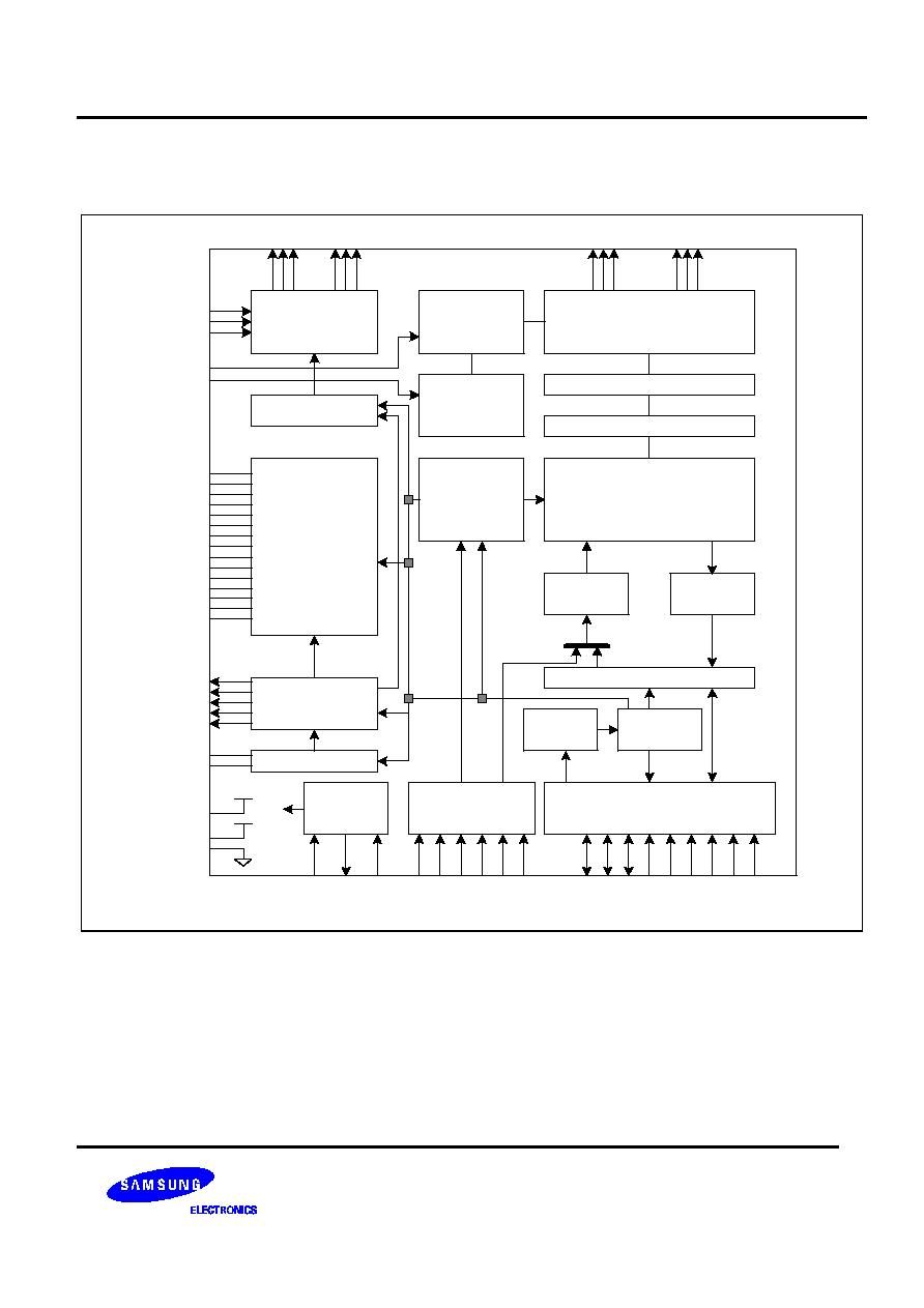
BLOCK DIAGRAM
396 CH.
Source Driver
Built-in GRAM
132x18x176 = 418,176 bit
OSC
System Interface
18/16/9/8-bit parallel, 3-pin SPI
178 CH.
Gate Driver
VDD3
VSS
Timing
Generator
Write data
latch
Control
register
M/AC circuit
Latch circuit
Grayscale
voltage
generator
Gamma
adjusting
circuit
Built-in
Power
Supply
circuit
Address
counter
Read data
latch
Bit operation
Index
register
Gate control
/ 72
/ 72
/ 18
/ 18
/ 18
/72
VCI
CL1
M
FLM
EQ
DISPTMG
OSC1
OSC2
Power
Regulator
GVDD
AVDD
VCI1/2/3/4
VBS
VGS
CVSS
AVSS
VCL
VREG1
VREG1OUT
VREG2
VREG2OUT
REGP/REGN
VCOMH/L/R
VCOMOUT
VGOFFH/L
VGOFFOUT
PRegB
RDVDD
VDD3
VDD
/ 2
/ 3
/ 2
VGH
VGL
Vgoff
DB0/SDI
DB1/SDO
DB[17:2]
R/W
E
RS
CSB
IM[3:0]
RESETB
/16
/ 4
/ 4
G177
G176
G175
.. .. .. ..
.. .. ..
G2
G1
G0
S396
S395
S394
S3
S2
S1
External
Display
Interface
VSYNC
HSYNC
DOTCLK
ENABLE
PD17-0
/ 18
PDSB
/ 18
/ 18
Figure 1. S6D0114 Block Diagram

132-RGB X 176-DOT 1-CHIP DRIVER IC FOR 262,144-COLOR TFT-LCD DISPLAY
S6D0114
Preliminary
6
PAD CONFIGURATION
G109
S1
G107
G0
G1
G99
G121
G161
DUMMY
C31+
C31-
VGL
G97
DUMMY
DUMMY
2530 um
20640 um
CVSS
VCL
VSS
IM0/ID
VDD3O
IM1
VSSO
IM2
VDD3O
PREGB
VDD3O
RESETB2
IM3
VSSO
DB15
DB14
DB13
DB12
DB11
DB17
DB16
DOTCLK
VSSO
VSYNC
HSYNC
VDD3O
ENABLE
PD17
PD16
PD15
VSSO
VDD3O
PDSB
C31+
C31-
VGL
VGL
VGL
VCL
CVSS
CVSS
VSS
DB10
DB9
DB8
VSSO
DB7
DB6
DB5
DB4
DB3
DB2
DB1/SDO
DB0/SDI
VSSO
RD
WR/SCL
RS
CS
VLD
VSSO
PD14
PD13
PD12
PD11
PD10
PD9
PD8
PD7
PD6
PD5
PD4
PD3
PD2
PD1
PD0
G3
G5
G7
G9
G101
DUMMY
DUMMY
G105
G103
G163
G165
G167
G169
G171
G173
G175
DUMMY
DUMMY
DUMMY
DUMMY
DUMMY
DUMMY
DUMMY
S2
S3
S4
S5
S6
S7
S8
NDT_OUT
DUMMY
DUMMY
G119
G117
G115
G113
G111
(with no S/L)
(with no S/L)
DUMMY
VCOMOUT
RESETB1
VGH
VGH
VCI3
C23+
C23-
C23-
C22+
C22-
C21+
C21-
C41+
C41+
C41-
VCOMOUT
DUMMY
DUMMY
DUMMY
DUMMY
VCI3
C23+
C22+
C22-
C21+
C21-
C41-
Figure 2. Pad Configuration

S6D0114 132-RGB X 176-DOT 1-CHIP DRIVER IC FOR 262,144-COLOR TFT-LCD DISPLAY
Preliminary
7
DUMMY
DUMMY
DUMMY
AVSS
VSSO
S6D0114
X
Y
(0,0)
VSSO
VCOMOUT
RESETB3
DUMMY
AVSS
AVSS
AVSS
VDD3O
VSSO
O_VSS
VDD3O
RVDD
RVDD
O_VDD
M_VDD
VDD
VDD
VCI
VCI4
OSC1
VDD
VDD
VBS
VCI
VCI
VCI
VCI
OSC2
VDD3
VDD3
VDD3
CL1
M
FLM
EQ
DISPTMG
VGS
VGS
VSS
VSS
VCOML
VSS
VSS
M_VDD
M_VDD
VSSO
CVSS
CVSS
M_VSS
M_VSS
M_VSS
VCOMH
VCI1
VCI1
VCI1
VCOMR
VREG1OUT
VREG1
GVDD
GVDD
VCI1
REGP
REGN
VCI2
AVDD
AVDD
VCI3
C11-
C11-
C11-
C11-
C11+
C11+
C11+
C11+
C12-
C12-
C12-
C12-
C12+
C12+
C12+
C12+
VGOFF
VCOML
VCI3
GVDD
AVDD
AVDD
VGOFFOUT
VGOFFH
VGOFFL
VREG2OUT
VREG2
VGOFF
VGOFFOUT
VGOFFH
VGOFFL
VREG2
VREG2OUT
DUMMY
DUMMY
DUMMY
DUMMY
VCOMOUT
G2
G4
G6
G8
G10
G104
G106
G102
G100
G98
S396
G164
G108
DUMMY
DUMMY
DUMMY
G110
G112
G114
G116
G118
G120
G122
G124
G166
G168
G170
G172
G174
G176
G177
DUMMY
DUMMY
DUMMY
DUMMY
DUMMY
DUMMY
DUMMY
DUMMY
S395
S394
S393
S392
S391
S390
S389
Figure 3. Pad Configuration (continued)
132-RGB X 176-DOT 1-CHIP DRIVER IC FOR 262,144-COLOR TFT-LCD DISPLAY
S6D0114
Preliminary
8
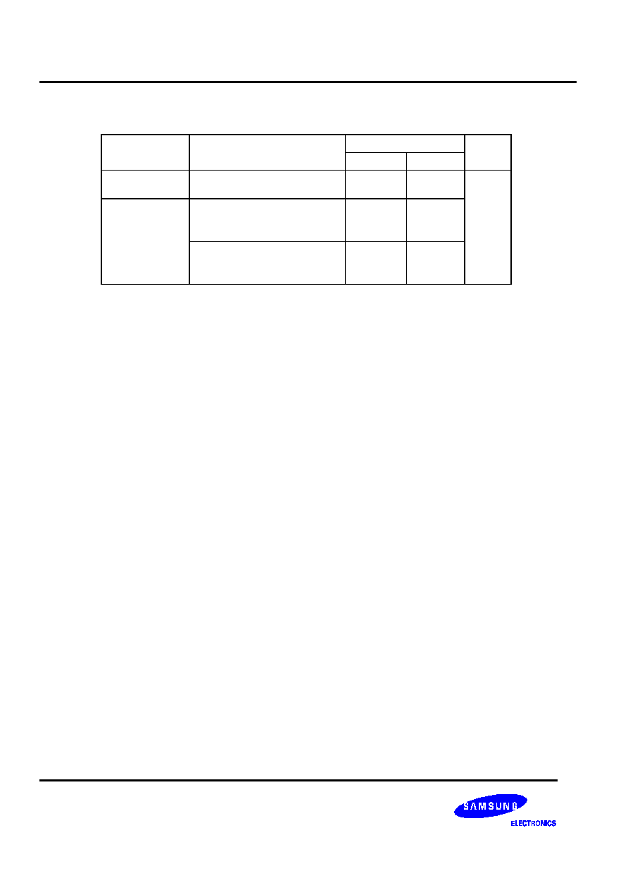
Table 1. S6D0114 Pad Dimensions
Size
Items
Pad name.
X
Y
Unit
Chip size
1)
-
20640
2530
INPUT PAD
54
100
Pad size
OUTPUT PAD
36
70
um
NOTES:
Scribe line is not included in this chip size (Scribe line: 120um)

S6D0114 132-RGB X 176-DOT 1-CHIP DRIVER IC FOR 262,144-COLOR TFT-LCD DISPLAY
Preliminary
9
ALIGN KEY CONFIGURATION AND COORDINATE
T.B.D
Figure 4. COG and ILB align key

132-RGB X 176-DOT 1-CHIP DRIVER IC FOR 262,144-COLOR TFT-LCD DISPLAY
S6D0114
Preliminary
10
T.B.D
Figure 5. Bump align key and align key configuration

S6D0114 132-RGB X 176-DOT 1-CHIP DRIVER IC FOR 262,144-COLOR TFT-LCD DISPLAY
Preliminary
11
PAD CENTER COORDINATES
Table 2. Pad Center Coordinates
[Unit: um]
(T.B.D)

132-RGB X 176-DOT 1-CHIP DRIVER IC FOR 262,144-COLOR TFT-LCD DISPLAY
S6D0114
Preliminary
12
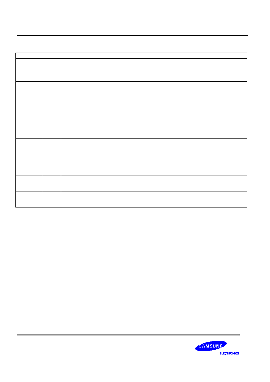
PIN DESCRIPTION
POWER SUPPLY PIN
Table 3. Power supply pin description
Symbol
I/O
Description
VDD
I /
Power
System power supply.
As S6D0114 has internal regulator, VDD range varies with each mode.
Non-regulated mode (PregB = 1) : +1.8 ~ +2.5 V
Regulated mode (PregB = 0) : +1.9V
VDD3
I /
Power
System power supply for regulator as external power.
(VDD3: +2.5 ~ +3.3 V)
AVDD
O /
Power
A power output pin for source driver block that is generated from power block.
Connect a capacitor for stabilization. (AVDD: +3.5 ~ +5.5 V)
Interconnect this pin to VCI2 pin.
GVDD
I /
Power
A Standard level for grayscale voltage generator.
Connect a capacitor for stabilization. When internal GVDD generator is not used,
connect an external power supply, AVDD � 0.5 V
VCI
I /
Power
An internal reference power supply for VREG1OUT/VREG2OUT.
Connect VDD when VDD = 2.5 to 3.3 V.
Connect a 2.5 to 3.3 V external-voltage power supply when VDD = 1.8 to 2.5 V.
VSS
I /
Power
System ground (0V)
CVSS
I /
Power
System ground level for step up circuit block.
AVSS
I /
Power
System ground level for analog circuit block.
VGS
I /
Power
Reference voltage for gamma voltage generator.
VCI1
Power
A reference voltage in step-up circuit 1.
Connect a capacitor for stabilization.
VCI2
Power
A reference voltage in step-up circuit 2.
VCI3
Power
A reference voltage in step-up circuit 3.
VCI4
Power
A reference voltage in step-up circuit 4. Connect VCI, VDD, or external power supply
lower than 3.3 V.
VCL
Power
A power supply pin for generating VcomL. When VcomL is higher than VSS, outputs
VSS level.

S6D0114 132-RGB X 176-DOT 1-CHIP DRIVER IC FOR 262,144-COLOR TFT-LCD DISPLAY
Preliminary
13
Table 4. Power supply pin description (continued)
Symbol
I/O
Description
VBS
I
Reference voltage for step-up circuit3.
REGN,
REGP
I/O
Input pins for reference voltages of VREG1OUT, and VREG2OUT when the internal
reference-voltage generation circuit is not used. Leave these pins open when the internal
reference-voltage generation circuit is used.
VREG1OUT
O
This pin outputs a reference voltage for VREG1 between AVDD and VSS. When the
internal reference voltage is not used, the reference voltage can be generated from the
voltage of REGP. Connect this pin to VREG1 and a capacitor for stabilization. When this
pin is not used, leave it open.
VREG2OUT
O
This pin outputs a reference voltage for VREG2 between VSS and VGL When the internal
reference voltage is not used, the reference voltage can be generated from the voltage of
REGN. Connect this pin to VREG2 and a capacitor for stabilizatio0n. When this pin is not
used, leave it open.
VcomOUT
O
A power supply for the TFT-display counter electrode.
The alternating cycle can be set by the M pin. Connect this pin to the TFT-display counter
electrode.
This pin is also used as equalizing function: When EQ = "High" period, all source driver's
outputs (S1 to S396) are short to Vcom level (Hi-z). In case of VcomL < 0V, equalizing
function must not be used. (Set EQ bit (R07h) to be "00" for preventing the abnormal
function.)
VcomR
I
A reference voltage of VcomH.
When VcomH is externally adjusted, halt the internal adjuster of VcomH by setting the
register and insert a variable resistor between GVDD and VSS. When this pin is not
externally adjusted, leave it open and adjust VcomH by setting the internal register.
VcomH
O
This pin indicates a high level of Vcom generated in driving the Vcom alternation.
Connect this pin to the capacitor for stabilization.
VcomL
O
When the Vcom alternation is driven, this pin indicates a low level of Vcom. An internal
register can be used to adjust the voltage. Connect this pin to a capacitor for stabilization.
When the VCOMG bit is low, the VcomL output stops and a capacitor for stabilization is not
needed.
VGH
O/
Power
A positive power output pin for gate driver, internal step-up circuits, bias circuits, and
operational amplifiers. Connect a capacitor for stabilization.
Interconnect this pin to VCI3 pin.
VGL
O/
Power
A Negative power output pin for gate driver, bias circuits, and operational amplifiers.
Connect a capacitor for stabilization. When internal VGL generator is not used, connect an
external-voltage power supply higher than -15.0 V.
132-RGB X 176-DOT 1-CHIP DRIVER IC FOR 262,144-COLOR TFT-LCD DISPLAY
S6D0114
Preliminary
14
Table 5. Power supply pin description (continued)
Symbol
I/O
Description
Vgoff
I
Power supply pin for off level for gate of TFT.
Connect VgoffOUT and a capacitor for stabilization. When VgoffOUT is not used, connect
an external-voltage power supply higher than -TBD V.
VgoffOUT
O
An power output pin for gate driver.
This pin is a negative voltage for the gate off level. Alternation can be synchronized by M
pin. Set the internal register according to the structure of the TFT-display retention volume.
For the amplitude at the alternation driving, this pin outputs a voltage between VcomH and
VcomL with the VgoffL reference voltage..
VgoffH
O
When the Vgoff alternation is driven, this pin indicates a high level of Vgoff. Connect a
capacitor for stabilization. When the CAD bit is low, the VgoffH output stops and a capacitor
for stabilization is not needed.
VgoffL
O
When the Vgoff alternation is driven, this pin indicates a low level of Vgoff. Connect a
capacitor for stabilization. An internal register can be used to adjust the voltage.
C11+,C11-
~
C23+,C23-
-
Connect the step-up capacitor according to the step-up factor.
C31+ ,
C31-
-
Connect a step-up capacitor for generating the VGL level.
C41+ ,
C41-
-
Connect a step-up capacitor for generating the -VCL level.
S6D0114 132-RGB X 176-DOT 1-CHIP DRIVER IC FOR 262,144-COLOR TFT-LCD DISPLAY
Preliminary
15
SYSTEM INTERFACE PIN
Table 6. System interface pin description
Symbol
I/O
Description
Selects the MPU interface mode:
IM3
IM2
IM1
IM0/ID
MPU interface mode
DB PIN assign
VSS
VSS
VSS
VSS
68-system 16-bit bus interface
DB17-10, DB8-1
VSS
VSS
VSS
VDD
68-system 8bit bus interface
DB17-10
VSS
VSS
VDD
VSS
80-system 16bit bus interface
DB17-10, DB8-1
VSS
VSS
VDD
VDD
80-system 8bit bus interface
DB17-10
VSS
VDD
VSS
ID
Serial peripheral interface (SPI)
DB1-0
VSS
VDD
VDD
*
Non-selecting
-
VDD
VSS
VSS
VSS
68-system 18-bit bus interface
DB17-0
VDD
VSS
VSS
VDD
68-system 9bit bus interface
DB17-9
VDD
VSS
VDD
VSS
80-system 18bit bus interface
DB17-0
VDD
VSS
VDD
VDD
80-system 9bit bus interface
DB17-9
VDD
VDD
*
*
Non-selecting
-
IM3-1,
IM0/ID
I
When a SPI mode is selected, the IM0 pin is used as ID setting bit for a device code.
CSB
I
Chip select signal input pin.
Low: S6D0114 is selected and can be accessed
High: S6D0114 is not selected and cannot be accessed
Must be fixed at VSS level when not used.
RS
I
Register select pin.
Low: Index/status, High: Control
IM2
IM1
Pin func.
MPU type
Pin description
VSS
VSS
E
68-system
Read/Write operation enable pin.
VSS
VDD
/WR
80-system
Write strobe signal input pin.
Data is fetched at the low level.
E
(/WR,SCL)
I
VDD
VSS
SCL
serial peripheral
interface
(SPI)
the synchronous clock signal input pin
IM2
IM1
Pin func.
MPU type
Pin description
VSS
VSS
R/W
68-system
Read/Write operation selection pin.
Low: Write , High: Read
VSS
VDD
/RD
80-system
Read strobe signal input pin.
Read out data at the low level.
R/W
(/RD)
I
When SPI mode is selected, fix this pin at VSS level.
DB0/SDI
I/O
Bi-directional data bus.
18-bit interface : DB 17-0
16-bit interface : DB 17-10, DB 8-1
9-bit interface : DB 17-9
8-bit interface : DB 17-10
Fix DB0 to the VDD3 or VSS level if the pin is not in use.
For a serial peripheral interface (SPI), input data is fetched at the rising edge of the SCL
signal.
132-RGB X 176-DOT 1-CHIP DRIVER IC FOR 262,144-COLOR TFT-LCD DISPLAY
S6D0114
Preliminary
16
Table 7. System interface pin description (Continued)
DB1/SDO
I/O
Bi-directional data bus.
18-bit interface : DB 17-0
16-bit interface : DB 17-10, DB 8-1
9-bit interface : DB 17-9
8-bit interface : DB 17-10
Fix DB1 to the VDD3 or VSS level if the pin is not in use.
For a serial peripheral interface (SPI), serves as the serial data output pin (SDO).
Successive bits are output at the falling edge of the SCL signal.
DB17-DB2
I/O
Bi-directional data bus.
18-bit interface : DB 17-0
16-bit interface : DB 17-10, DB 8-1
9-bit interface : DB 17-9
8-bit interface : DB 17-10
Fix unused pin to the VDD3 or VSS level.
Data input valid signal when GRAM is written:
CSB
VLD
GRAM write
GRAM address
0
0
Valid
Update
0
1
Invalid
Update
1
*
Invalid
Storage
VLD
I
Fix VLD pin at VSS level if the pin is not used.
Data enable signal pin for RGB interface.
High: the IC can be access via RGB interface.
Low: the IC cannot be access via RGB interface
ENABLE
VLD
GRAM write
GRAM address
1
0
Valid
Update
1
1
Invalid
Update
0
*
Invalid
Storage
ENABLE
I
Fix ENABLE pin at VDD3 level if the pin is not used.
VSYNC
I
Synchronous signal of frame.
Low: active
Fix VSYNC pin at VDD3 level if the pin is not used.
HSYNC
I
Synchronous signal of line.
Low: active
Fix HSYNC pin at VDD3 level if the pin is not used.
DOTCLK
I
Input pin for dot clock.
PD17-PD0
I
RGB data input bus.
18-bit interface : PD 17-0
16-bit interface : PD 17-13, PD 11-1
6-bit interface : PD 17-12
Fix unused pin to the VDD3 or VSS level.
PDSB
I
RGB and SYSTEM interface hold DB17-0 pin in common as a data input pin when PDSB
pin is "low".
RESETB1/
RESETB2/
RESETB3
I
Reset pin. Initializes the LSI when low. Must be reset after power-on.
S6D0114 132-RGB X 176-DOT 1-CHIP DRIVER IC FOR 262,144-COLOR TFT-LCD DISPLAY
Preliminary
17
DISPLAY PIN
Table 8. Display pin description
Symbol
I/O
Description
S1 - S396
O
Source driver output pins.
The SS bit can change the shift direction of the source signal.
For example, if SS = 0, gray data of S1 is read from RAM address 0000h.
If SS = 1, contents of is RAM address 0000h is out from S396.
S1, S4, S7, ... S(3n-1) : display Red (R) (SS = 0)
S2, S5, S8, ... S(3n-2) : display Green (G) (SS = 0)
S3, S6, S9, ... S(3n) : display Blue (B) (SS = 0)
G1 - G176
O
Gate driver output pins.
The output of driving circuit is whether VGH or Vgoff.
VGH : gate-ON level
Vgoff : gate-OFF level
G0,
G177
O
Gate driver output pins for IC maker's testing.
Please, leave it disconnected.
CL1
O
Output pin for raster-row clock pulse.
M
O
Output pin for AC-cycle signal.
FLM
O
Output pin for frame-start pulse.
EQ
O
Output pin for timing for equalizing.
Low : Normal display, High : Equalizing
DISPTMG
O
Output pin for Gate off signal.
High : Normal output
Low : Non-display
MISCELLANEOUS CONTROL PIN
Table 9. Oscillator and internal power regulator pin description
Symbol
I/O
Description
OSC1/
OSC2
I/O
Connect an external resistor for R-C oscillation.
When input the clock from outside, input to OSC1, and open OSC2.
PregB
I
Internal power regulator control input pin.
When the internal regulated power (RDVDD) is used as VDD, PregB is fixed to "low" level.
When the external logic power(VDD3) is used as VDD, PregB is fixed to "high" level.
RDVDD
O
Internal power regulated-VDD output (typ. 1.8V).
When PregB is "low", RDVDD is connected to VDD pin. When PRegB is "high", leave this
pin open.
132-RGB X 176-DOT 1-CHIP DRIVER IC FOR 262,144-COLOR TFT-LCD DISPLAY
S6D0114
Preliminary
18
FUNCTIONAL DESCRIPTION
SYSTEM INTERFACE
The S6D0114 has five high-speed system interfaces: an 80-system 18-/16-/9-/8-bit bus, a 68-system 18-/16-/9-/8-
bit bus, and a serial interface (SPI: Serial Peripheral Interface). The IM3-0 pins select the interface mode.
The S6D0114 has three 18-bit registers: an index register (IR), a write data register (WDR), and a read data register
(RDR). The IR stores index information for control register and GRAM. The WDR temporarily stores data to be
written into control register and GRAM. The RDR temporarily stores data read from GRAM. Data written into the
GRAM from MPU is initially written to the WDR and then written to the GRAM automatically. Data is read through the
RDR when reading from the GRAM, and the first read data is invalid and the second and the following data are valid.
When a logic operation is performed inside of the S6D0114 by using the display data stored in the GRAM and the
data written from the MPU, the data read through the RDR is used. Accordingly, the MPU does not need to read data
twice or to fetch the read data into the MPU. This enables high-speed processing.
Execution time for instruction, except oscillation start, is 0-clock cycle so that instructions can be written in
succession.
Table 10. Register Selection (18-/16-/9-/8- Parallel Interface)
SYSTEM
R/W
/WR
E
/RD
RS
Operations
0
1
0
Write index to IR
1
1
0
Read internal status
0
1
1
Write to control register and GRAM through WDR
68
1
1
1
Read from GRAM through RDR
0
1
0
Write index to IR
1
0
0
Read internal status
0
1
1
Write to control register and GRAM through WDR
80
1
0
1
Read from GRAM through RDR
Table 11. CSB/VLD signal (GRAM update control)
CSB
VLD
Operation
0
0
Data is written to GRAM, GRAM address is updated
1
0
Data is not written to GRAM, GRAM address is not updated
0
1
Data is not written to GRAM, GRAM address is updated
1
1
Data is not written to GRAM, GRAM address is not updated
Table 12. Register Selection (Serial Peripheral Interface)
R/W bit
RS bit
Operation
0
0
Write index to IR
1
0
Read internal status
0
1
Write data to control register and GRAM through WDR
1
1
Read data from GRAM through RDR

S6D0114 132-RGB X 176-DOT 1-CHIP DRIVER IC FOR 262,144-COLOR TFT-LCD DISPLAY
Preliminary
19
EXTERNAL INTERFACE (RGB-I/F, VSYNC-I/F)
The S6D0114 incorporates RGB and VSYNC interface as external interface for motion picture display.
When the RGB interface is selected, the synchronization signals (VSYNC, HSYNC, and DOTCLK) are available for
display. The RGB data for display (PD17-0) are written according to enable signal (ENABLE) and data valid signal
(VLD) in synchronization with VSYNC, HSYNC, and DOTCLK signal. This allows flicker-free updating of the screen.
When the VSYNC interface is selected, internal operation is normally synchronized with internal clock except
operation related to frame synchronization: It is synchronized with the VSYNC signal. The data for display are
written to GRAM via conventional system interface. There are some limitations on the timing and methods for writing
to GRAM in VSYNC interface. See the section on the external display interface.
BIT OPERATION
The S6D0114 supports the following functions: a write data mask function that selects and writes data to GRAM in
bit unit, a logic operation function that performs logic operations or conditional determination on the display data set
in GRAM and writes to GRAM. These functions can greatly reduce the processing loads of the MPU graphics
software and can rewrite the display data in the GRAM at high speed. For details, see the Graphics Operation
Function section.
ADDRESS COUNTER (AC)
The address counter (AC) assign address to GRAM. When an address-set-instruction is written to the IR, the
address information is sent from IR to AC. After writing to the GRAM, the address value of AC is automatically
increased/decreased by 1 according to ID1-0 bit of control register. After reading data from GRAM, the AC is not
updated. A window address function allows data to be written only to a window area specified by GRAM.
GRAPHICS RAM (GRAM)
The graphics RAM (GRAM) has 18-bits/pixel and stores the bit-pattern data for 132-RGB x 176-dot display.
GRAYSCALE VOLTAGE GENERATOR
The grayscale voltage circuit generates a certain voltage level that is specified by the grayscale
-adjusting resistor
for LCD driver circuit. By use of the generator, 262,144 colors can be displayed at the same time. For details, see the
-adjusting resistor section.
TIMING GENERATOR
The timing generator generates timing signals for the operation of internal circuits such as GRAM.
The GRAM read timing for display and the internal operation timing for MPU access is generated separately to avoid
interference with one another. Several important timing signals can be monitored via signal monitoring pin (M, FLM,
CL1, EQ, DISPTMG).
OSCILLATION CIRCUIT (OSC)
The S6D0114 can provide R-C oscillation simply through the addition of an external oscillation-resistor between the
OSC1 and OSC2 pin. The appropriate oscillation frequency for operating voltage, display size, and frame frequency

132-RGB X 176-DOT 1-CHIP DRIVER IC FOR 262,144-COLOR TFT-LCD DISPLAY
S6D0114
Preliminary
20
can be obtained by adjusting the external-resistor value. Clock pulse can also be supplied externally. Since R-C
oscillation stops during the standby mode, current consumption can be reduced. For details, see the Oscillation
Circuit section.
SOURCE DRIVER CIRCUIT
The liquid crystal display source driver circuit consists of 396 drivers (S1 to S396).
Display pattern data is latched when 396-bit data has arrived. The latched data then enables the source drivers to
generate drive waveform outputs. The SS bit can change the shift direction of 396-bit data by selecting an
appropriate direction for the device-mounted configuration.
GATE DRIVER CIRCUIT
The liquid crystal display gate driver circuit consists of 178 gate drivers (G0 to G177).
The VGH or Vgoff level is output by the signal from the gate control circuit. G0 and G177 are IC maker's test pins.
S6D0114 132-RGB X 176-DOT 1-CHIP DRIVER IC FOR 262,144-COLOR TFT-LCD DISPLAY
Preliminary
21
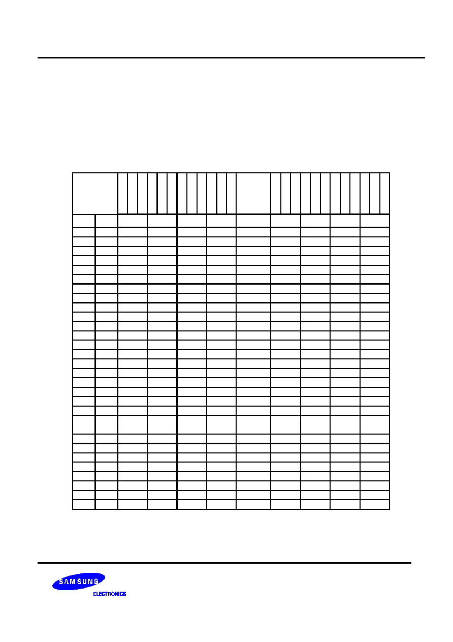
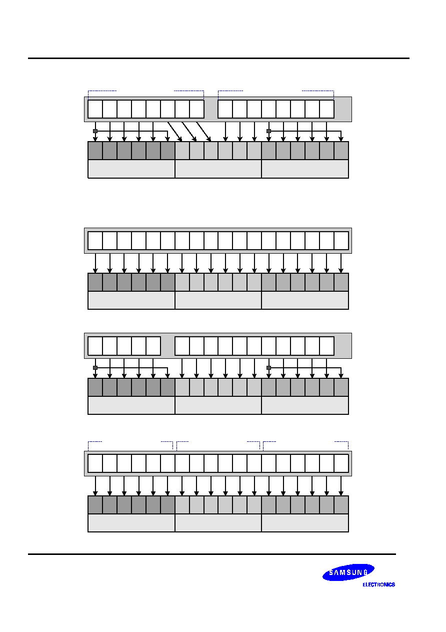
SYSTEM/RGB INTERFACE AND GRAM ADDRESS SETTING
GRAM ADDRESS SETTING (SS="0")
When SS bit is 0 (source output shift direction: right) and BGR bit is 0 (RGB sequence: right) that can be set in R01h
register, GRAM address is set as follows:
Table 13. GRAM address (SS="0")
S1
S2
S3
S4
S5
S6
S7
S8
S9
S10
S11
S12
... ... ...
S385
S386
S387
S388
S389
S390
S391
S392
S393
S394
S395
S396
DB
DB DB
DB DB
DB DB
DB
DB
DB DB
DB DB
DB DB
DB
18
0
18
0
18
0
18
0
18
0
18
0
18
0
18
0
G1
G176
... ... ...
G2
G175
... ... ...
G3
G174
... ... ...
G4
G173
... ... ...
G5
G172
... ... ...
G6
G171
... ... ...
G7
G170
... ... ...
G8
G169
... ... ...
G9
G168
... ... ...
G10
G167
... ... ...
G11
G166
... ... ...
G12
G165
... ... ...
G13
G164
... ... ...
G14
G163
... ... ...
G15
G162
... ... ...
G16
G161
... ... ...
G17
G160
... ... ...
G18
G159
... ... ...
G19
G158
... ... ...
G20
G157
... ... ...
G169
G168
... ... ...
G170
G167
... ... ...
G171
G166
... ... ...
G172
G165
... ... ...
G173
G164
... ... ...
G174
G163
... ... ...
G175
G162
... ... ...
G176
G161
... ... ...
S/G Output
GS=0 GS=1
... ...
... ...
"0000"H
"0001"H
"0002"H
"0003"H
"0100"H
"0101"H
"0102"H
"0103"H
"0200"H
"0201"H
"0202"H
"0203"H
"0300"H
"0301"H
"0302"H
"0303"H
"0400"H
"0401"H
"0402"H
"0403"H
"0500"H
"0501"H
"0502"H
"0503"H
"0600"H
"0601"H
"0602"H
"0603"H
"0700"H
"0701"H
"0702"H
"0703"H
"0800"H
"0801"H
"0802"H
"0803"H
"0900"H
"0901"H
"0902"H
"0903"H
"0A00"H
"0A01"H
"0A02"H
"0A03"H
"0B00"H
"0B01"H
"0B02"H
"0B03"H
"0C00"H
"0C01"H
"0C02"H
"0C03"H
"0D00"H
"0D01"H
"0D02"H
"0D03"H
"0E00"H
"0E01"H
"0E02"H
"0E03"H
"0F00"H
"0F01"H
"0F02"H
"0F03"H
"1000"H
"1001"H
"1002"H
"1003"H
"1100"H
"1101"H
"1102"H
"1103"H
"1200"H
"1201"H
"1202"H
"1203"H
......
......
......
"1300"H
......
......
......
"1301"H
"1302"H
"1303"H
... ...
... ...
"A800"H
"A801"H
"A802"H
"A803"H
"A900"H
"A901"H
"A902"H
"A903"H
"AA00"H
"AA01"H
"AA02"H
"AA03"H
"AB00"H
"AB01"H
"AB02"H
"AB03"H
"AC00"H
"AC01"H
"AC02"H
"AC03"H
"AD00"H
"AD01"H
"AD02"H
"AD03"H
"AE00"H
"AE01"H
"AE02"H
"AE03"H
"AF00"H
"AF01"H
"AF02"H
"AF03"H
... ...
... ...
... ...
... ...
"0080"H
"0081"H
"0082"H
"0083"H
"0180"H
"0181"H
"0182"H
"0183"H
"0280"H
"0281"H
"0282"H
"0283"H
"0380"H
"0381"H
"0382"H
"0383"H
"0480"H
"0481"H
"0482"H
"0483"H
"0580"H
"0581"H
"0582"H
"0583"H
"0680"H
"0681"H
"0682"H
"0683"H
"0780"H
"0781"H
"0782"H
"0783"H
"0880"H
"0881H
"0882"H
"0883"H
"0980"H
"0981"H
"0982"H
"0983"H
"0A80"H
"0A81"H
"0A82"H
"0A83"H
"0B80"H
"0B81"H
"0B82"H
"0B83"H
"0C80"H
"0C81"H
"0C82"H
"0C83"H
"0D80"H
"0D81"H
"0D82"H
"0D83"H
"0E80"H
"0E81"H
"0E82"H
"0E83"H
"0F80"H
"0F81"H
"0F82"H
"0F83"H
"1080"H
"1081"H
"1082"H
"1083"H
"1180"H
"1181"H
"1182"H
"1183"H
"1280"H
"1281"H
"1282"H
"1283"H
"1380"H
"1381"H
"1382"H
"1383"H
......
......
......
......
"A880"H
"A881"H
"A880"H
"A883"H
"A980"H
"A981"H
"A980"H
"A983"H
"AA80"H
"AA81"H
"AA80"H
"AA83"H
"AB80"H
"AB81"H
"AB80"H
"AB83"H
"AC80"H
"AC81"H
"AC80"H
"AC83"H
"AD80"H
"AD81"H
"AD80"H
"AD83"H
"AE80"H
"AE81"H
"AE80"H
"AE83"H
"AF80"H
"AF81"H
"AF80"H
"AF83"H

132-RGB X 176-DOT 1-CHIP DRIVER IC FOR 262,144-COLOR TFT-LCD DISPLAY
S6D0114
Preliminary
22
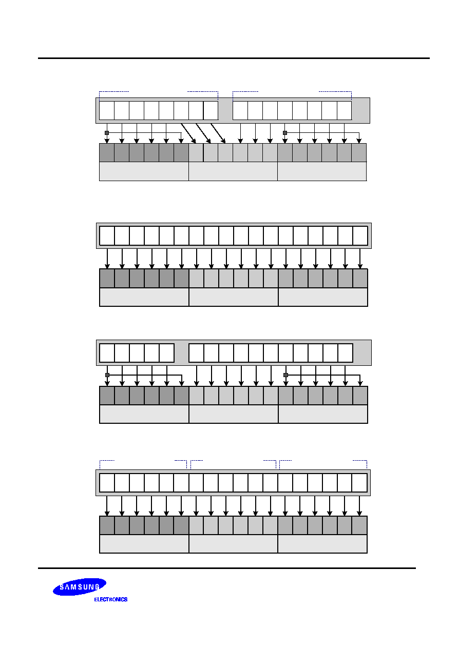
Data fetch from GRAM for display when SS=0 is shown in the following figure.
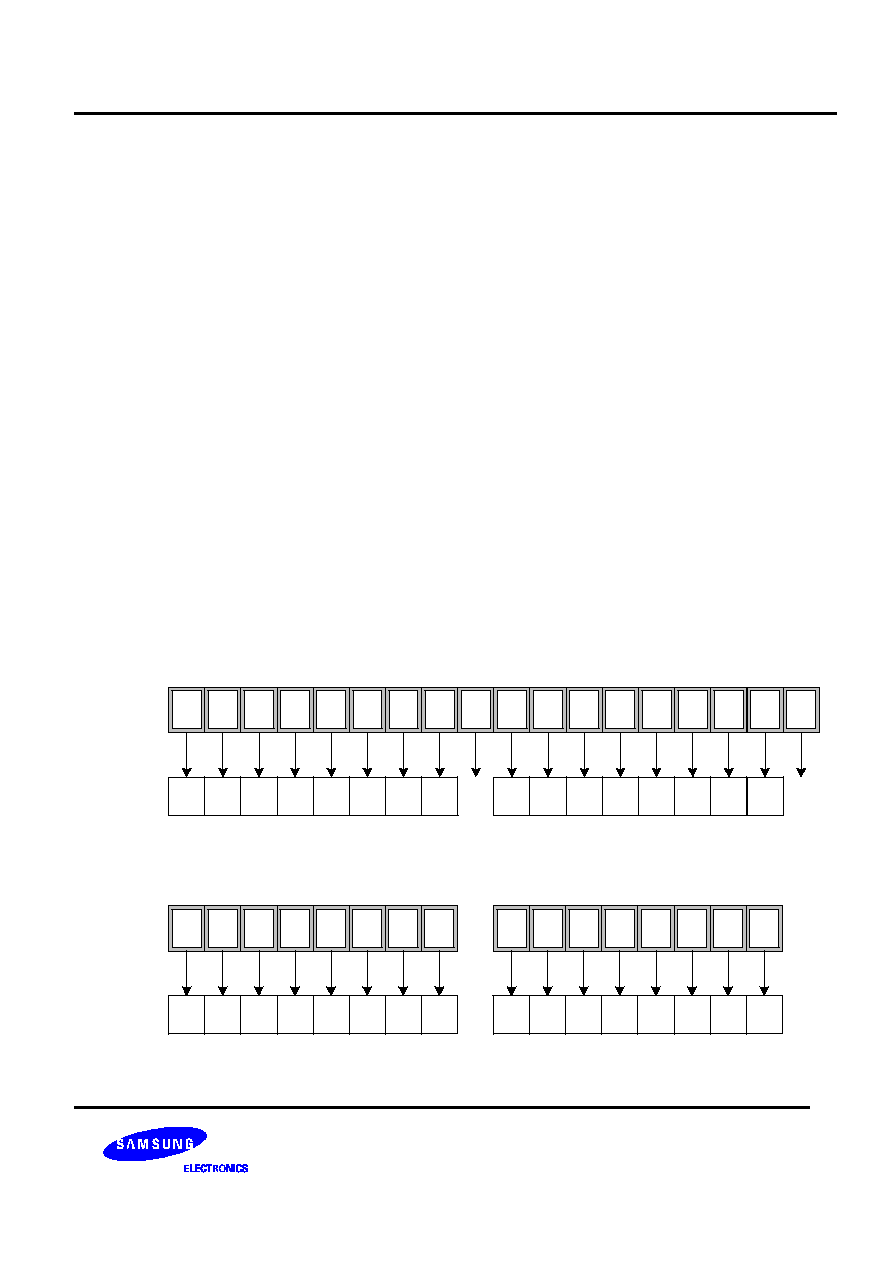
SYSTEM INTERFACE
80-system 18-bit interface
DB
17
DB
16
DB
15
DB
14
DB
13
DB
12
DB
11
DB
10
DB
9
DB
8
DB
7
DB
6
DB
5
DB
4
DB
3
DB
2
DB
1
DB
0
GRAM DATA
R5
R4
R3
R2
R1
R0
S (3n + 1)
G5 G4 G3 G2 G1 G0
S (3n + 2)
B5
B4
B3
B2 B1
B0
S (3n + 3)
RGB Arrangement
Output
Note: n= lower 8 byte of address (0 to 175)
80-system 16-bit interface
DB
17
DB
16
DB
15
DB
14
DB
13
DB
12
DB
11
DB
10
DB
8
DB
7
DB
6
DB
5
DB
4
DB
3
DB
2
DB
1
GRAM DATA
R5
R4
R3
R2
R1
R0
S (3n + 1)
G5 G4 G3 G2 G1 G0
S (3n + 2)
B5
B4
B3
B2 B1
B0
S (3n + 3)
RGB Arrangement
Output
Note: n= lower 8 byte of address (0 to 175)
80-system 9-bit interface
DB
17
DB
16
DB
15
DB
14
DB
13
DB
12
DB
11
DB
10
DB
9
GRAM DATA
R5
R4
R3
R2
R1
R0
S (3n + 1)
G5 G4 G3 G2 G1 G0
S (3n + 2)
B5
B4
B3
B2 B1
B0
S (3n + 3)
RGB Arrangement
Output
Note: n= lower 8 byte of address (0 to 175)
1st Transmission
DB
17
DB
16
DB
15
DB
14
DB
13
DB
12
DB
11
DB
10
DB
9
2nd Transmission
S6D0114 132-RGB X 176-DOT 1-CHIP DRIVER IC FOR 262,144-COLOR TFT-LCD DISPLAY
Preliminary
23
80-system 8-bit interface/SPI
DB
17
DB
16
DB
15
DB
14
DB
13
DB
12
DB
11
DB
10
DB
17
DB
16
DB
15
DB
14
DB
13
DB
12
DB
11
DB
10
GRAM DATA
R5
R4
R3
R2
R1
R0
S (3n + 1)
G5 G4
G3 G2
G1 G0
S (3n + 2)
B5
B4
B3
B2
B1
B0
S (3n + 3)
RGB Arrangement
Output
Note: n= lower 8 byte of address (0 to 175)
1st Transmission
2nd Transmission
RGB INTERFACE
18-bit RGB interface
PD
17
PD
16
PD
15
PD
14
PD
13
PD
12
PD
11
PD
10
PD
9
PD
8
PD
7
PD
6
PD
5
PD
4
PD
3
PD
2
PD
1
PD
0
GRAM DATA
R5
R4
R3
R2
R1
R0
S (3n + 1)
G5 G4 G3 G2 G1 G0
S (3n + 2)
B5
B4
B3
B2
B1
B0
S (3n + 3)
RGB Arrangement
Output
Note: n= lower 8 byte of address (0 to 175)
16-bit RGB interface
PD
17
PD
16
PD
15
PD
14
PD
13
PD
9
PD
11
PD
10
PD
8
PD
7
PD
6
PD
5
PD
4
PD
3
PD
2
PD
1
GRAM DATA
R5
R4
R3
R2
R1
R0
S (3n + 1)
G5 G4 G3 G2 G1 G0
S (3n + 2)
B5
B4
B3
B2
B1
B0
S (3n + 3)
RGB Arrangement
Output
Note: n= lower 8 byte of address (0 to 175)
6-bit RGB interface
DB
17
DB
16
DB
15
DB
14
DB
13
DB
12
GRAM DATA
R5
R4
R3
R2
R1
R0
S (3n + 1)
G5 G4 G3 G2 G1 G0
S (3n + 2)
B5
B4
B3
B2 B1
B0
S (3n + 3)
RGB Arrangement
Output
Note: n= lower 8 byte of address (0 to 175)
1st Transmission
2nd Transmission
3rd Transmission
DB
17
DB
16
DB
15
DB
14
DB
13
DB
12
DB
17
DB
16
DB
15
DB
14
DB
13
DB
12
132-RGB X 176-DOT 1-CHIP DRIVER IC FOR 262,144-COLOR TFT-LCD DISPLAY
S6D0114
Preliminary
24
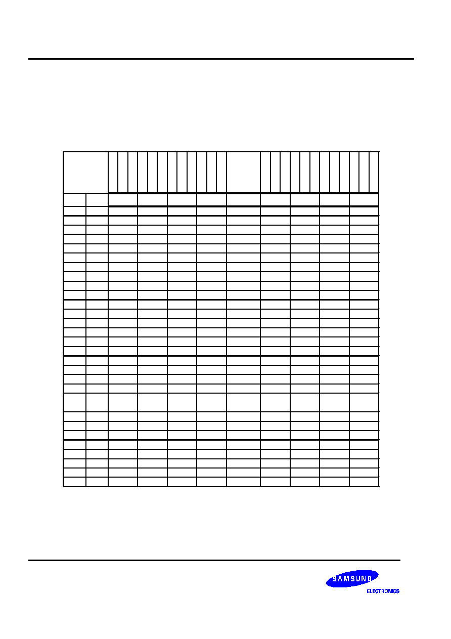
GRAM ADDRESS SETTING (SS="1")
When SS bit is 1 (source output shift direction: reversed) and BGR bit is 1 (RGB sequence: reversed) that can be set
in R01h register, GRAM address is set as follows:
Table 14. GRAM address (SS="1")
S1
S2
S3
S4
S5
S6
S7
S8
S9
S10
S11
S12
... ... ...
S385
S386
S387
S388
S389
S390
S391
S392
S393
S394
S395
S396
DB
DB DB
DB DB
DB DB
DB
DB
DB DB
DB DB
DB DB
DB
18
0
18
0
18
0
18
0
18
0
18
0
18
0
18
0
G1
G176
... ... ...
G2
G175
... ... ...
G3
G174
... ... ...
G4
G173
... ... ...
G5
G172
... ... ...
G6
G171
... ... ...
G7
G170
... ... ...
G8
G169
... ... ...
G9
G168
... ... ...
G10
G167
... ... ...
G11
G166
... ... ...
G12
G165
... ... ...
G13
G164
... ... ...
G14
G163
... ... ...
G15
G162
... ... ...
G16
G161
... ... ...
G17
G160
... ... ...
G18
G159
... ... ...
G19
G158
... ... ...
G20
G157
... ... ...
G169
G168
... ... ...
G170
G167
... ... ...
G171
G166
... ... ...
G172
G165
... ... ...
G173
G164
... ... ...
G174
G163
... ... ...
G175
G162
... ... ...
G176
G161
... ... ...
S/G Output
GS=0 GS=1
... ...
... ...
... ...
... ...
... ...
... ...
... ...
... ...
"0083"H
"0082"H
"0081"H
"0080"H
"0003"H
"0002"H
"0001"H
"0000"H
"0183"H
"0182"H
"0181"H
"0180"H
"0103"H
"0102"H
"0101"H
"0100"H
"0283"H
"0282"H
"0281"H
"0280"H
"0203"H
"0202"H
"0201"H
"0200"H
"0383"H
"0382"H
"0381"H
"0380"H
"0303"H
"0302"H
"0301"H
"0300"H
"0483"H
"0482"H
"0481"H
"0480"H
"0403"H
"0402"H
"0401"H
"0400"H
"0583"H
"0582"H
"0581"H
"0580"H
"0503"H
"0502"H
"0501"H
"0500"H
"0683"H
"0682"H
"0681"H
"0680"H
"0603"H
"0602"H
"0601"H
"0600"H
"0783"H
"0782"H
"0781"H
"0780"H
"0703"H
"0702"H
"0701"H
"0700"H
"0883"H
"0882"H
"0881H
"0880"H
"0803"H
"0802"H
"0801"H
"0800"H
"0983"H
"0982"H
"0981"H
"0980"H
"0903"H
"0902"H
"0901"H
"0900"H
"0A83"H
"0A82"H
"0A81"H
"0A80"H
"0A03"H
"0A02"H
"0A01"H
"0A00"H
"0B83"H
"0B82"H
"0B81"H
"0B80"H
"0B03"H
"0B02"H
"0B01"H
"0B00"H
"0C83"H
"0C82"H
"0C81"H
"0C80"H
"0C03"H
"0C02"H
"0C01"H
"0C00"H
"0D83"H
"0D82"H
"0D81"H
"0D80"H
"0D03"H
"0D02"H
"0D01"H
"0D00"H
"0E83"H
"0E82"H
"0E81"H
"0E80"H
"0E03"H
"0E02"H
"0E01"H
"0E00"H
"0F83"H
"0F82"H
"0F81"H
"0F80"H
"0F03"H
"0F02"H
"0F01"H
"0F00"H
"1083"H
"1082"H
"1081"H
"1080"H
"1003"H
"1002"H
"1001"H
"1000"H
"1183"H
"1182"H
"1181"H
"1180"H
"1103"H
"1102"H
"1101"H
"1100"H
"1283"H
"1282"H
"1281"H
"1280"H
"1203"H
"1202"H
"1201"H
"1200"H
"1302"H
"1301"H
"1300"H
"1383"H
"1382"H
"1381"H
"1380"H
......
......
......
"1303"H
......
......
......
......
......
......
"A880"H
"A881"H
"A880"H
"A803"H
"A802"H
"A801"H
......
"A800"H
"A983"H
"A980"H
"A981"H
"A980"H
"A903"H
"A902"H
"A901"H
"A900"H
"A883"H
"AA83"H
"AA80"H
"AA81"H
"AA80"H
"AA03"H
"AA02"H
"AA01"H
"AA00"H
"AB83"H
"AB80"H
"AB81"H
"AB80"H
"AB03"H
"AB02"H
"AB01"H
"AB00"H
"AC83"H
"AC80"H
"AC81"H
"AC80"H
"AC03"H
"AC02"H
"AC01"H
"AC00"H
"AD83"H
"AD80"H
"AD81"H
"AD80"H
"AD03"H
"AD02"H
"AD01"H
"AD00"H
"AE83"H
"AE80"H
"AE81"H
"AE80"H
"AE03"H
"AE02"H
"AE01"H
"AE00"H
"AF83"H
"AF80"H
"AF81"H
"AF80"H
"AF03"H
"AF02"H
"AF01"H
"AF00"H
S6D0114 132-RGB X 176-DOT 1-CHIP DRIVER IC FOR 262,144-COLOR TFT-LCD DISPLAY
Preliminary
25
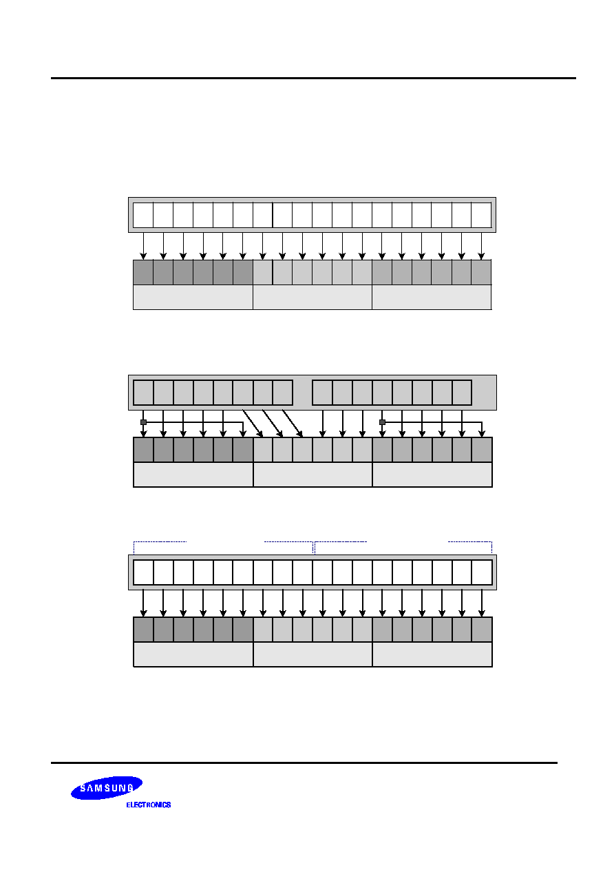
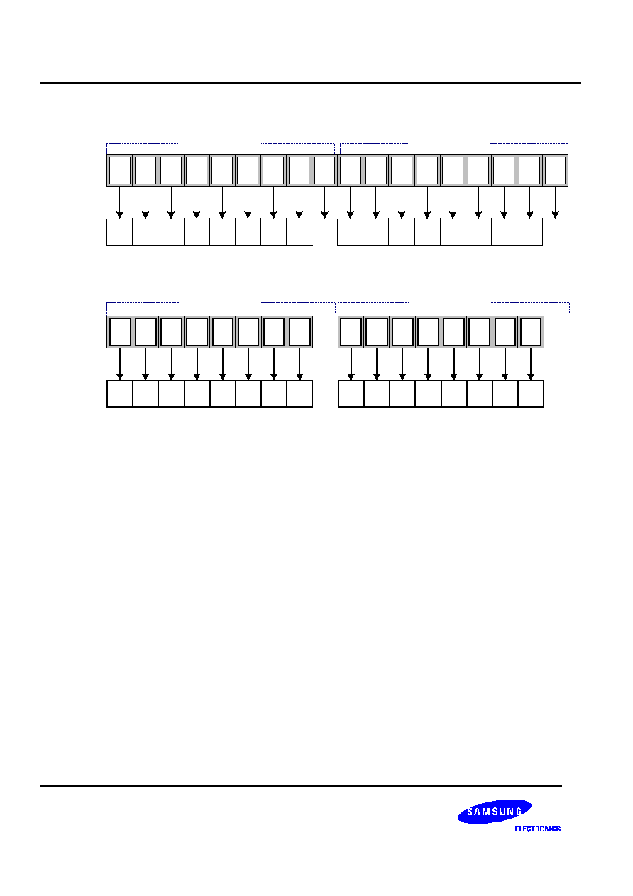
Data fetch from GRAM for display when SS=1 is shown in the following figure.
SYSTEM INTERFACE
80-system 18-bit interface
DB
17
DB
16
DB
15
DB
14
DB
13
DB
12
DB
11
DB
10
DB
9
DB
8
DB
7
DB
6
DB
5
DB
4
DB
3
DB
2
DB
1
DB
0
GRAM DATA
R5
R4
R3
R2
R1
R0
S (396-3n)
G5 G4 G3 G2 G1 G0
S (395-3n)
B5
B4
B3
B2
B1
B0
S (394-3n)
RGB Arrangement
Output
Note: n= lower 8 byte of address (0 to 175)
80-system 16-bit interface
DB
17
DB
16
DB
15
DB
14
DB
13
DB
12
DB
11
DB
10
DB
8
DB
7
DB
6
DB
5
DB
4
DB
3
DB
2
DB
1
GRAM DATA
R5
R4
R3
R2
R1
R0 G5 G4 G3 G2 G1 G0 B5
B4
B3
B2 B1
B0
RGB Arrangement
Output
Note: n= lower 8 byte of address (0 to 175)
S (396-3n)
S (395-3n)
S (394-3n)
80-system 9-bit interface
DB
17
DB
16
DB
15
DB
14
DB
13
DB
12
DB
11
DB
10
DB
9
GRAM DATA
R5
R4
R3
R2
R1
R0
G5 G4
G3 G2
G1 G0
B5
B4
B3
B2
B1
B0
RGB Arrangement
Output
Note: n= lower 8 byte of address (0 to 175)
1st Transmission
DB
17
DB
16
DB
15
DB
14
DB
13
DB
12
DB
11
DB
10
DB
9
2nd Transmission
S (396-3n)
S (395-3n)
S (394-3n)
132-RGB X 176-DOT 1-CHIP DRIVER IC FOR 262,144-COLOR TFT-LCD DISPLAY
S6D0114
Preliminary
26
80-system 8-bit interface
DB
17
DB
16
DB
15
DB
14
DB
13
DB
12
DB
11
DB
10
DB
17
DB
16
DB
15
DB
14
DB
13
DB
12
DB
11
DB
10
GRAM DATA
R5
R4
R3
R2
R1
R0
G5 G4
G3 G2
G1 G0
B5
B4
B3
B2
B1
B0
RGB Arrangement
Output
Note: n= lower 8 byte of address (0 to 175)
1st Transmission
2nd Transmission
S (396-3n)
S (395-3n)
S (394-3n)
RGB INTERFACE
18-bit interface
PD
17
PD
16
PD
15
PD
14
PD
13
PD
12
PD
11
PD
10
PD
9
PD
8
PD
7
PD
6
PD
5
PD
4
PD
3
PD
2
PD
1
PD
0
GRAM DATA
R5
R4
R3
R2
R1
R0 G5 G4 G3 G2 G1 G0 B5
B4
B3
B2 B1
B0
RGB Arrangement
Output
Note: n= lower 8 byte of address (0 to 175)
S (396-3n)
S (395-3n)
S (394-3n)
16-bit interface
PD
17
PD
16
PD
15
PD
14
PD
13
PD
9
PD
11
PD
10
PD
8
PD
7
PD
6
PD
5
PD
4
PD
3
PD
2
PD
1
GRAM DATA
R5
R4
R3
R2
R1
R0 G5 G4 G3 G2 G1 G0 B5
B4
B3
B2 B1
B0
RGB Arrangement
Output
Note: n= lower 8 byte of address (0 to 175)
S (396-3n)
S (395-3n)
S (394-3n)
6-bit interface
DB
17
DB
16
DB
15
DB
14
DB
13
DB
12
GRAM DATA
R5
R4
R3
R2
R1
R0
G5 G4
G3 G2
G1 G0
B5
B4
B3
B2
B1
B0
RGB Arrangement
Output
Note: n= lower 8 byte of address (0 to 175)
1st Transmission
2nd Transmission
3rd Transmission
DB
17
DB
16
DB
15
DB
14
DB
13
DB
12
DB
17
DB
16
DB
15
DB
14
DB
13
DB
12
S (396-3n)
S (395-3n)
S (394-3n)
S6D0114 132-RGB X 176-DOT 1-CHIP DRIVER IC FOR 262,144-COLOR TFT-LCD DISPLAY
Preliminary
27
INSTRUCTIONS
The S6D0114 uses the 18-bit bus architecture. Before the internal operation of the S6D0114 starts, control
information is temporarily stored in the registers described below to allow high-speed interfacing with a high-
performance microcomputer. The internal operation of the S6D0114 is determined by signals sent from the
microcomputer. These signals, which include the register selection signal (RS), the read/write signal (R/W), and the
data bus signals (DB17 to DB0), make up the S6D0114 instructions.
There are nine categories of instructions that:
-
Specify the index
-
Read the status
-
Control the display
-
Control power management
-
Process the graphics data
-
Set internal GRAM addresses
-
Transfer data to and from the internal GRAM
-
Set grayscale level for the internal grayscale palette table
-
Interface with the gate driver and power supply IC
Normally, instructions that write data are used the most. However, an auto-update of internal GRAM addresses after
each data write can lighten the microcomputer program load. As instructions are executed in 0 cycles, they can be
written in succession.
The 16-bit instruction assignment differ from interface-setup (18-/16-/9-/8-/SPI), so instructions should be fetched
according to the data format shown below:
80-system 18-bit Interface
DB
17
INPUT DATA
Instruction Bit
(IB)
DB
16
DB
15
DB
14
DB
13
DB
12
DB
11
DB
10
DB
9
DB
8
DB
7
DB
6
DB
5
DB
4
DB
3
DB
2
DB
1
DB
0
IB
15
IB
14
IB
13
IB
12
IB
11
IB
10
IB
9
IB
8
IB
7
IB
6
IB
5
IB
4
IB
3
IB
2
IB
1
IB
0
80-system 16-bit Interface
DB
17
INPUT DATA
Instruction Bit
(IB)
DB
16
DB
15
DB
14
DB
13
DB
12
DB
11
DB
10
DB
8
DB
7
DB
6
DB
5
DB
4
DB
3
DB
2
DB
1
IB
15
IB
14
IB
13
IB
12
IB
11
IB
10
IB
9
IB
8
IB
7
IB
6
IB
5
IB
4
IB
3
IB
2
IB
1
IB
0
132-RGB X 176-DOT 1-CHIP DRIVER IC FOR 262,144-COLOR TFT-LCD DISPLAY
S6D0114
Preliminary
28
80-system 9-bit Interface
1st Transmission
2nd Transmission
DB
17
INPUT DATA
Instruction Bit
(IB)
DB
16
DB
15
DB
14
DB
13
DB
12
DB
11
DB
10
DB
9
DB
8
DB
7
DB
6
DB
5
DB
4
DB
3
DB
2
DB
1
DB
0
IB
15
IB
14
IB
13
IB
12
IB
11
IB
10
IB
9
IB
8
IB
7
IB
6
IB
5
IB
4
IB
3
IB
2
IB
1
IB
0
80-system 8-bit Interface/SPI (2-transfer per pixel)
DB
17
INPUT DATA
Instruction Bit
(IB)
DB
16
DB
15
DB
14
DB
13
DB
12
DB
11
DB
10
DB
8
DB
7
DB
6
DB
5
DB
4
DB
3
DB
2
DB
1
IB
15
IB
14
IB
13
IB
12
IB
11
IB
10
IB
9
IB
8
IB
7
IB
6
IB
5
IB
4
IB
3
IB
2
IB
1
IB
0
1st Transmission
2nd Transmission
S6D0114 132-RGB X 176-DOT 1-CHIP DRIVER IC FOR 262,144-COLOR TFT-LCD DISPLAY
Preliminary
29
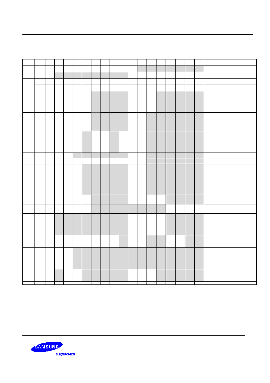
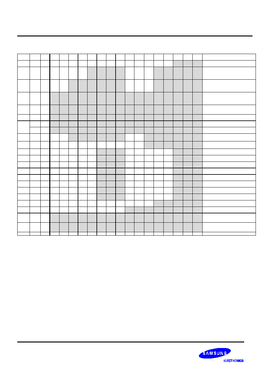
Instruction Table
Table 15. Instruction table 1
Reg.
No
R/W
RS
DB
15
DB
14
DB
13
DB
12
DB
11
DB
10
DB
9
DB
8
DB
7
DB
6
DB
5
DB
4
DB
3
DB
2
DB
1
DB
0
Register Name /
Description
IR
0
0
*
*
*
*
*
*
*
*
*
ID6
ID5
ID4
ID3
ID2
ID1
ID0
Index /
Sets the index register value
SR
1
0
L7
L6
L5
L4
L3
L2
L1
L0
0
0
0
0
0
0
0
0
Status read /
Reads the internal status of the S6D0114
0
1
*
*
*
*
*
*
*
*
*
*
*
*
*
*
*
1
Start oscillation(R00H) /
Starts the oscillation circuit
R00h
1
1
0
0
0
0
0
0
0
1
0
0
0
1
0
1
0
0
Device code read /
Read 0114H
R01h
0
1
0
0
0
0
EPL
SM
GS
SS
0
0
0
NL4
NL3
NL2
NL1
NL0
Driver output control(R01H) /
EPL: set polarity of ENABLE pin while
using RGB interface.
SM: gate driver division drive control
GS: gate driver shift direction
SS: source driver shift direction
NL4-0: number of driving lines
R02h
0
1
0
0
0
0
FLD1 FDL0
B/C
EOR
0
0
NW5
NW4
NW3
NW2
NW1
NW0
LCD-Driving-waveform control (R02H)/
FLD1-0: number of interlaced field
B/C: LCD drive AC waveform
EOR: Exclusive OR-ing the AC waveform
NW5-0: number of n-raster-row of C-
pattern
R03h
0
1
0
0
0
BGR
0
0
HWM
0
0
0
I/D1
I/D0
AM
LG2
LG1
LG0
Entry mode(R03H) /
BGR: RGB swap control
HWM: high-speed RAM write
I/D1-0: address counter Increment /
Decrement control
AM: horizontal / vertical RAM update
LG2-0: Logic operation control
R04h
0
1
0
0
CP11 CP10
CP9
CP8
CP7
CP6
0
0
CP5
CP4
CP3
CP2
CP1
CP0 Compare register 1(R04H)/
R05h
0
1
0
0
0
0
0
0
0
0
0
0
CP17 CP16 CP15 CP14 CP13 CP12 Compare register 2(R05H)/
R07h
0
1
0
0
0
PT1
PT0
VLE2 VLE1
SPT
0
0
GON
DTE
CL
REV
D1
D0
Display control (R07H) /
PT1-0: Non-display area source output
control
VLE2-1: 1
st
/2
nd
partial vertical scroll
SPT: 1
st
/2
nd
partial display enable
GON: gate-off to be VSS level
DTE:DISPTMG to be VSS level
CL: 8-color display mode enable
REV: display area inversion drive
D1-0: source output control
R08h
0
1
0
0
0
0
FP3
FP2
FP1
FP0
0
0
0
0
BP3
BP2
BP1
BP0
Blank period control 1 (R08H)/
BP3-0: Back porch setting
FP3-0: Front porch setting
R09h
0
1
0
0
0
0
BLP1
3
BLP1
2
BLP1
1
BLP1
0
BLP2
3
BLP2
2
BLP2
1
BLP2
0
0
0
0
0
Blank period control 2 (R09H)/
BLP1: blanking period setting
BLP2: blanking period setting
R0Bh
0
1
NO1
NO0 SDT1 SDT0 EQ1
EQ0
DIV1
DIV0
0
0
0
0
RTN3 RTN2 RTN1 RTN0
Frame cycle control (R0BH)/
NO1-0: specify the amount of non-overlap
SDT1-0: set amount of source delay
EQ1-0: equalizing period setting
DVI1-0: division ratio of internal clock
setting
RTN3-0: set the 1-H period
R0Ch
0
1
0
0
0
0
0
0
0
RM
0
0
DM1
DM2
0
0
RIM0
RIM1
External interface control(R0CH) /
RM: specify the interface for RAM access
DM2-1: specify display operation mode
RIM1-0: specify RGB-I/F mode
R10h
0
1
0
0
SAP2 SAP1 SAP0
BT2
BT1
BT0
DC2
DC1
DC0
AP2
AP1
AP0
SLP
STB
Power control 1 (R10H) /
SAP2-0:
BT2-0:
DC2-0:
AP2-0:
SLP:
STB:
R11h
0
1
CAD
0
0
VRN4 VRN3 VRN2 VRN1 VRN0
0
0
0
VRP4 VRP3 VRP2 VRP1 VRP0
Power control 2 (R11H)/
CAD:
VRN4-0:
VRP4-0:
132-RGB X 176-DOT 1-CHIP DRIVER IC FOR 262,144-COLOR TFT-LCD DISPLAY
S6D0114
Preliminary
30
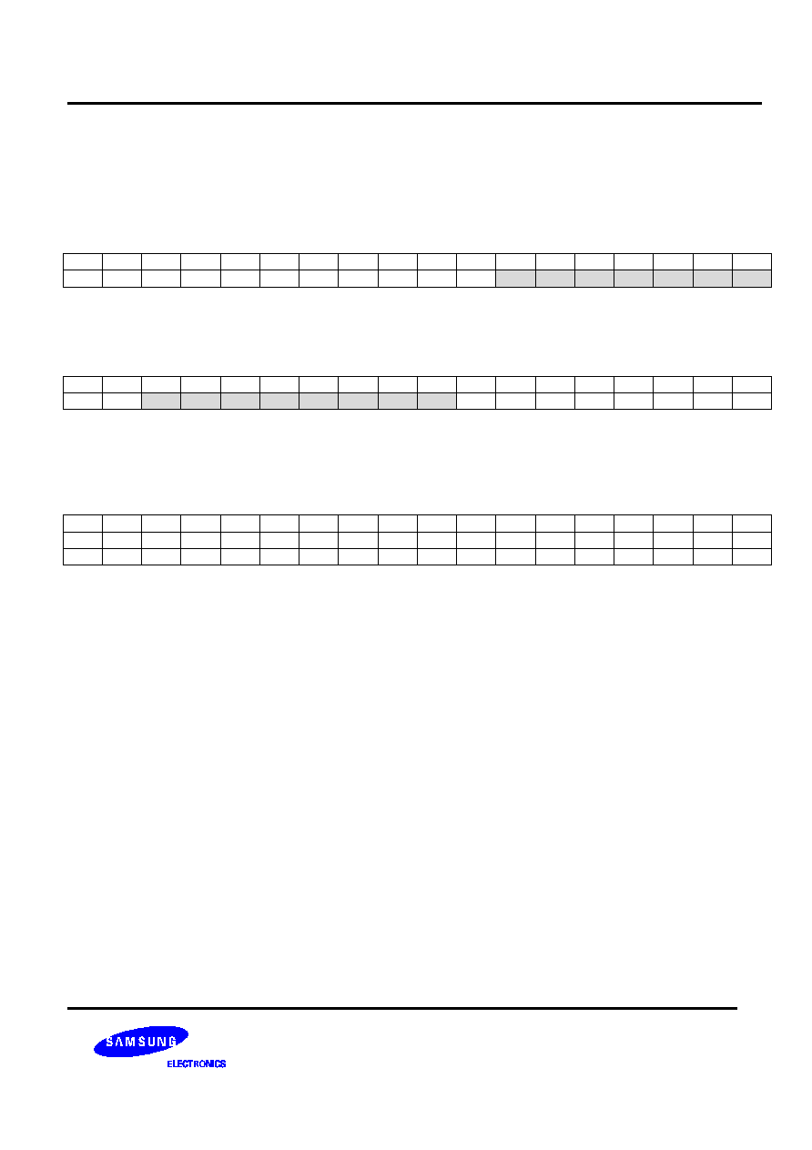
Table 16. Instruction table 2
Reg.
No
R/W
RS
DB
15
DB
14
DB
13
DB
12
DB
11
DB
10
DB
9
DB
8
DB
7
DB
6
DB
5
DB
4
DB
3
DB
2
DB
1
DB
0
Register Name /
Description
R12h
0
1
0
0
0
0
0
0
0
0
0
0
0
0
0
VC2
VC1
VC0
Power control 3 (R12H)/
VC2-0:
R13h
0
1
0
0
0
0
VRL3 VRL2 VRL1 VRL0
0
0
0
PON VRH3 VRH2 VRH1 VRH0
Power control 4 (R13H)/
PON:
VRL3-0:
VRH3-0:
R14h
0
1
0
0
VCO
MG
VDV4 VDV3 VDV2 VDV1 VDV0
0
0
0
VCM4 VCM3 VCM2 VCM1 VCM0
Power control 5 (R14H)/
VCOMG:
VDV4-0:
VCM4-0:
R16h
0
1
HEA7 HEA6 HEA5 HEA4 HEA3 HEA2 HEA1 HEA0 HSA7 HSA6 HSA5 HSA4 HSA3 HSA2 HSA1 HSA0
Horizontal RAM Address position
(R16H)/
HEA7-0:
HSA7-0
R17h
0
1
VEA7 VEA6 VEA5 VEA4 VEA3 VEA2 VEA1 VEA0 VSA7 VSA6 VSA5 VSA4 VSA3 VSA2 VSA1 VSA0
Vertical RAM Address position (R17H)/
HEA7-0:
HSA7-0
R21h
0
1
AD15 AD14 AD13 AD12 AD11 AD10
AD9
AD8
AD7
AD6
AD5
AD4
AD3
AD2
AD1
AD0
RAM address set (R21H)/
AD15-0:
0
1
WD15 WD14 WD13 WD12 WD11 WD10 WD9
WD8
WD7
WD6
WD5
WD4
WD3
WD2
WD1
WD0
Write data to GRAM (R22H)/
WD15-0:
R22h
1
1
RD15 RD14 RD13 RD12 RD11 RD10 RD9
RD8
RD7
RD6
RD5
RD4
RD3
RD2
RD1
RD0
Read data from GRAM (R22H)/
RD15-0:
R23h
0
1
0
0
WM11 WM10 WM9 WM8 WM7 WM6
0
0
WM5
WM4
WM3
WM2
WM1
WM0
RAM write data mask 1 (R23H)/
WM11-0:
R24h
0
1
0
0
0
0
0
0
0
0
0
0
WM17 WM16 WM15 WM14 WM13 WM12
RAM write data mask 2 (R24H)/
WM17-12:
R30h
0
1
0
0
0
0
0
PKP
12
PKP
11
PKP
10
0
0
0
0
0
PKP
02
PKP
01
PKP
00
Gamma control 1 (R30H)/
Adjust Gamma voltage
R31h
0
1
0
0
0
0
0
PKP
32
PKP
31
PKP
30
0
0
0
0
0
PKP
22
PKP
21
PKP
20
Gamma control 2 (R31H)/
Adjust Gamma voltage
R32h
0
1
0
0
0
0
0
PKP
52
PKP
51
PKP
50
0
0
0
0
0
PKP
42
PKP
41
PKP
40
Gamma control 3 (R32H)/
Adjust Gamma voltage
R33h
0
1
0
0
0
0
0
PRP
12
PRP
11
PRP
10
0
0
0
0
0
PRP
02
PRP
01
PRP
00
Gamma control 4 (R33H)/
Adjust Gamma voltage
R34h
0
1
0
0
0
0
0
PKN
12
PKN
11
PKN
10
0
0
0
0
0
PKN
02
PKN
01
PKN
00
Gamma control 5 (R34H)/
Adjust Gamma voltage
R35h
0
1
0
0
0
0
0
PKN
32
PKN
31
PKN
30
0
0
0
0
0
PKN
22
PKN
21
PKN
20
Gamma control 6 (R35H)/
Adjust Gamma voltage
R36h
0
1
0
0
0
0
0
PKN
52
PKN
51
PKN
50
0
0
0
0
0
PKN
42
PKN
41
PKN
40
Gamma control 7 (R36H)/
Adjust Gamma voltage
R37h
0
1
0
0
0
0
0
PRN
12
PRN
11
PRN
10
0
0
0
0
0
PRN
02
PRN
01
PRN
00
Gamma control 8 (R37H)/
Adjust Gamma voltage
R40h
0
1
0
0
0
0
0
0
0
0
0
0
0
SCN4 SCN3 SCN2 SCN1 SCN0
Gate scan position (R40H)/
SCN4-0: scan starting position of gate
R41h
0
1
0
0
0
0
0
0
0
0
VL7
VL6
VL5
VL4
VL3
VL2
VL1
VL0
Vertical scroll control (R41H)/
VL7-0:
R42h
0
1
SE17 SE16 SE15 SE14 SE13 SE12 SE11 SE10 SS17 SS16 SS15 SS14 SS13 SS12 SS11 SS10
1
st
screen driving position (R42H)/
SE17-10:
SS17-10
R43h
0
1
SE27 SE26 SE25 SE24 SE23 SE22 SE21 SE20 SS27 SS26 SS25 SS24 SS23 SS22 SS21 SS20
2
nd
screen driving position (R43H)/
SE27-20:
SS27-20
S6D0114 132-RGB X 176-DOT 1-CHIP DRIVER IC FOR 262,144-COLOR TFT-LCD DISPLAY
Preliminary
31
INSTRUCTION DESCRIPTIONS
Index
The index instruction specifies the RAM control indexes (R00h to R3Fh). It sets the register number in the range of
00000 to 111111 in binary form. However, R40 to R44 are disabled since they are test registers.
R/W
RS
DB15
DB14
DB13
DB12
DB11
DB10
DB9
DB8
DB7
DB6
DB5
DB4
DB3
DB2
DB1
DB0
W
0
*
*
*
*
*
*
*
*
*
ID6
ID5
ID4
ID3
ID2
ID1
ID0
Status Read
The status read instruction read out the internal status of the IC.
R/W
RS
DB15
DB14
DB13
DB12
DB11
DB10
DB9
DB8
DB7
DB6
DB5
DB4
DB3
DB2
DB1
DB0
R
0
L7
L6
L5
L4
L3
L2
L1
L0
0
0
0
0
0
0
0
0
L7�0:
Indicate the driving raster-row position where the liquid crystal display is being driven.
Start Oscillation (R00h)
R/W
RS
DB15
DB14
DB13
DB12
DB11
DB10
DB9
DB8
DB7
DB6
DB5
DB4
DB3
DB2
DB1
DB0
W
1
*
*
*
*
*
*
*
*
*
*
*
*
*
*
*
1
R
1
0
0
0
0
0
0
0
1
0
0
0
1
0
1
0
0
The start oscillation instruction restarts the oscillator from the Halt State in the standby mode. After this instruction,
wait at least 10 ms for oscillation to stabilize before giving the next instruction. (See the Standby Mode section)
If this register is read forcibly, *0114h is read.
132-RGB X 176-DOT 1-CHIP DRIVER IC FOR 262,144-COLOR TFT-LCD DISPLAY
S6D0114
Preliminary
32
Driver Output Control (R01h)
R/W
RS
DB15
DB14
DB13
DB12
DB11
DB10
DB9
DB8
DB7
DB6
DB5
DB4
DB3
DB2
DB1
DB0
W
1
0
0
0
0
EPL
SM
GS
SS
0
0
0
NL4
NL3
NL2
NL1
NL0
GS:
Selects the output shift direction of the gate driver. When GS = 0, G1 shifts to G176. When GS = 1, G176 shifts
to G1.
SM: Select the division drive method of the gate driver. When SM = 0, even/odd division is selected; SM = 1,
upper/lower division drive is selected. Various connections between TFT panel and the IC can be supported with the
combination of SM and GS bit.
SS:
Selects the output shift direction of the source driver. When SS = 0, S1 shifts to S396. When SS = 1, S396 shifts
to S1. In addition, SS and BGR bits should be specified in case of the RGB order is changed. When SS = 0 and BGR
= 0, <R><G><B> are assigned in order from S1 pin. When SS = 1 and BGR = 1, <R><G><B> are assigned in order
from S396. Re-write data to GRAM whenever SS and BGR bit are changed.
EPL: Set the polarity of ENABLE pin while using RGB interface.
EPL = "0": ENABLE = "Low" / write data of PD17-0
ENABLE = "High" / don't write data of PD17-0
EPL = "1": ENABLE = "High" / write data of PD17-0
ENABLE = "Low" / don't write data of PD17-0
Table 17. Relationship between EPL, ENABLE, VLD and RAM access
EPL
ENABLE
VLD
RAM write
RAM address
0
0
0
Valid
Updated
0
0
1
Invalid
Updated
0
1
*
Invalid
Held
1
1
0
Valid
Updated
1
1
1
Invalid
Updated
1
0
*
Invalid
Held

S6D0114 132-RGB X 176-DOT 1-CHIP DRIVER IC FOR 262,144-COLOR TFT-LCD DISPLAY
Preliminary
33
NL4�0:
Specify the number of raster-rows to be driven. The number of raster-row can be adjusted in units of eight.
GRAM address mapping is independent of this setting. The set value should be higher than the panel size.
Table 18. NL bit and Drive Duty (SCN4-0=00000)
NL4
NL3
NL2
NL1
NL0
Display size
Number of LCD driver lines
Gate driver used
0
0
0
0
0
Setting disabled
Setting disabled
Setting disabled
0
0
0
0
1
396 X 16 dots
16
G1 to G16
0
0
0
1
0
396 X 24 dots
24
G1 to G24
0
0
0
1
1
396 X 32 dots
32
G1 to G32
0
0
1
0
0
396 X 40 dots
40
G1 to G40
0
0
1
0
1
396 X 48 dots
48
G1 to G48
0
0
1
1
0
396 X 56 dots
56
G1 to G56
0
0
1
1
1
396 X 64 dots
64
G1 to G64
0
1
0
0
0
396 X 72 dots
72
G1 to G72
0
1
0
0
1
396 X 80 dots
80
G1 to G80
0
1
0
1
0
396 X 88 dots
88
G1 to G88
0
1
0
1
1
396 X 96 dots
96
G1 to G96
0
1
1
0
0
396 X 104 dots
104
G1 to G104
0
1
1
0
1
396 X 112 dots
112
G1 to G112
0
1
1
1
0
396 X 120 dots
120
G1 to G120
0
1
1
1
1
396 X 128 dots
128
G1 to G128
1
0
0
0
0
396 X 136 dots
136
G1 to G136
1
0
0
0
1
396 X 144 dots
144
G1 to G144
1
0
0
1
0
396 X 152 dots
152
G1 to G152
1
0
0
1
1
396 X 160 dots
160
G1 to G160
1
0
1
0
0
396 X 168 dots
168
G1 to G168
1
0
1
0
1
396 X 176 dots
176
G1 to G176
NOTE: A FP (front porch) and BP (back porch) period will be inserted as blanking period (All gates output Vgoff
level) before / after the driver scan through all of the scans.
132-RGB X 176-DOT 1-CHIP DRIVER IC FOR 262,144-COLOR TFT-LCD DISPLAY
S6D0114
Preliminary
34
LCD-Driving-Waveform Control (R02h)
R/W
RS
DB15
DB14
DB13
DB12
DB11
DB10
DB9
DB8
DB7
DB6
DB5
DB4
DB3
DB2
DB1
DB0
W
1
0
0
0
0
FLD
1
FLD
0
B/C
EOR
0
0
NW5
NW4
NW3
NW2
NW1
NW0
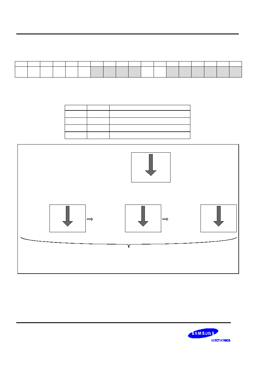
FLD1-0: These bits are for the set up of the interlaced driver's n raster-row. See the following table and figure for the
set up value and field raster-row and scanning method.
Table 19. Association chart for scanning FLD1-0 and n raster-row
FLD1
FLD0
Scanning method
0
0
Set up disabled
0
1
1 field
1
0
Set up disabled
1
1
3 field (interlaced)
G1
4
G2
4
G3
4
..... G174
4
G175
4
G176
TFT Panel
(a) When FLD1-0= 01(normal scanning)
G1
4
G4
4
G7
4
.....
4
G174
TFT Panel
G2
4
G5
4
G8
4
.....
4
G175
G3
4
G6
4
G9
4
.....
4
G176
TFT Panel
TFT Panel
1 frame
Frame 1/3
Frame 2/3
Frame 3/3
(b) When FLD1-0= 11(interlaced scanning)
Figure 6. n raster-row interlaced scanning method
B/C: When B/C = 0, a B-pattern waveform is generated and alternates at every frame. When B/C = 1, an n raster-
row AC waveform is generated and alternates in each raster-row specified by bits EOR and NW4�NW0 in the
LCD-driving-waveform control register (R02h). For details, see the n-raster-row Reversed AC Drive section.

S6D0114 132-RGB X 176-DOT 1-CHIP DRIVER IC FOR 262,144-COLOR TFT-LCD DISPLAY
Preliminary
35
EOR: When the C-pattern waveform is set (B/C = 1) and EOR = 1, the odd/even frame-select signals and the n-
raster-row reversed signals are EORed(Exclusive-OR) for alternating drive. EOR is used when the LCD is not
alternated by combining the set values of the number of the LCD drive raster-row and the n raster-row. For details,
see the n-raster-row Reversed AC Drive section.
NW5�0: Specify the number of raster-rows that will alternate in the C-pattern waveform setting (B/C = 1).
NW4�NW0 alternate for every set value + 1 raster-row, and the first to the 64th raster-rows can be selected.
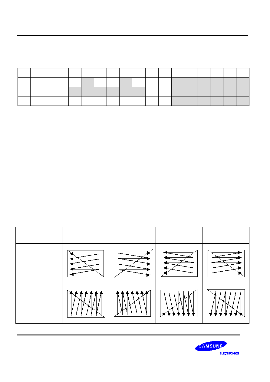
132-RGB X 176-DOT 1-CHIP DRIVER IC FOR 262,144-COLOR TFT-LCD DISPLAY
S6D0114
Preliminary
36
Entry Mode (R03h)
Compare Register 1 (R04h)
Compare Register 2 (R05h)
R/W
RS
DB15
DB14
DB13
DB12
DB11
DB10
DB9
DB8
DB7
DB6
DB5
DB4
DB3
DB2
DB1
DB0
W
1
0
0
0
BGR
0
0
HWM
0
0
0
I/D1
I/D0
AM
LG2
LG1
LG0
W
1
0
0
CP11
CP10
CP9
CP8
CP7
CP6
0
0
CP5
CP4
CP3
CP2
CP1
CP0
W
1
0
0
0
0
0
0
0
0
0
0
CP17
CP16
CP15
CP14
CP13
CP12
The write date sent from MPU is modified in the S6D0114 and written to the GRAM. The display data in the GRAM
can be quickly rewritten to reduce the load of the microcomputer software processing. For details, see the Graphics
Operation Function section.
HWM: When HWM=1, data can be written to the GRAM at high speed. In high-speed write mode, four words of data
are written to the GRAM in a single operation after writing to GRAM four times. Write to RAM four times, otherwise
the four words cannot be written to the GRAM. Thus, set the lower 2 bits to 0 when setting the RAM address.
For details, see the High Speed RAM Write Mode section.
I/D1-0: When I/D1-0 = 1, the address counter (AC) is automatically increased by 1 after the data is written to the
GRAM. When I/D1-0 = 0, the AC is automatically decreased by 1 after the data is written to the GRAM. Automatic
address counter updating is not performed when reading data from GRAM. The increment/decrement setting of the
address counter by I/D1-0 bits is performed independently for the upper (AD15-8) and lower (AD7-0) addresses.
The AM bit sets the direction of moving through the addresses when the GRAM is written.
AM: Set the automatic update method of the AC after the data is written to the GRAM. When AM = 0, the data is
continuously written in parallel. When AM = 1, the data is continuously written vertically. When window address
range is specified, the GRAM in the window address range can be written to according to the I/D1-0 and AM
settings.
Table 20. Address Direction Setting
I/D1-0="00"
H: decrement
V: decrement
I/D1-0="01"
H: increment
V: increment
I/D1-0="10"
H: decrement
V: increment
I/D1-0="11"
H: increment
V: increment
AM=0
Horizontal
0000h
AF83h
0000h
AF83h
0000h
AF83h
0000h
AF83h
AM=1
Vertical
0000h
AF83h
AF83h
0000h
AF83h
0000h
AF83h
0000h
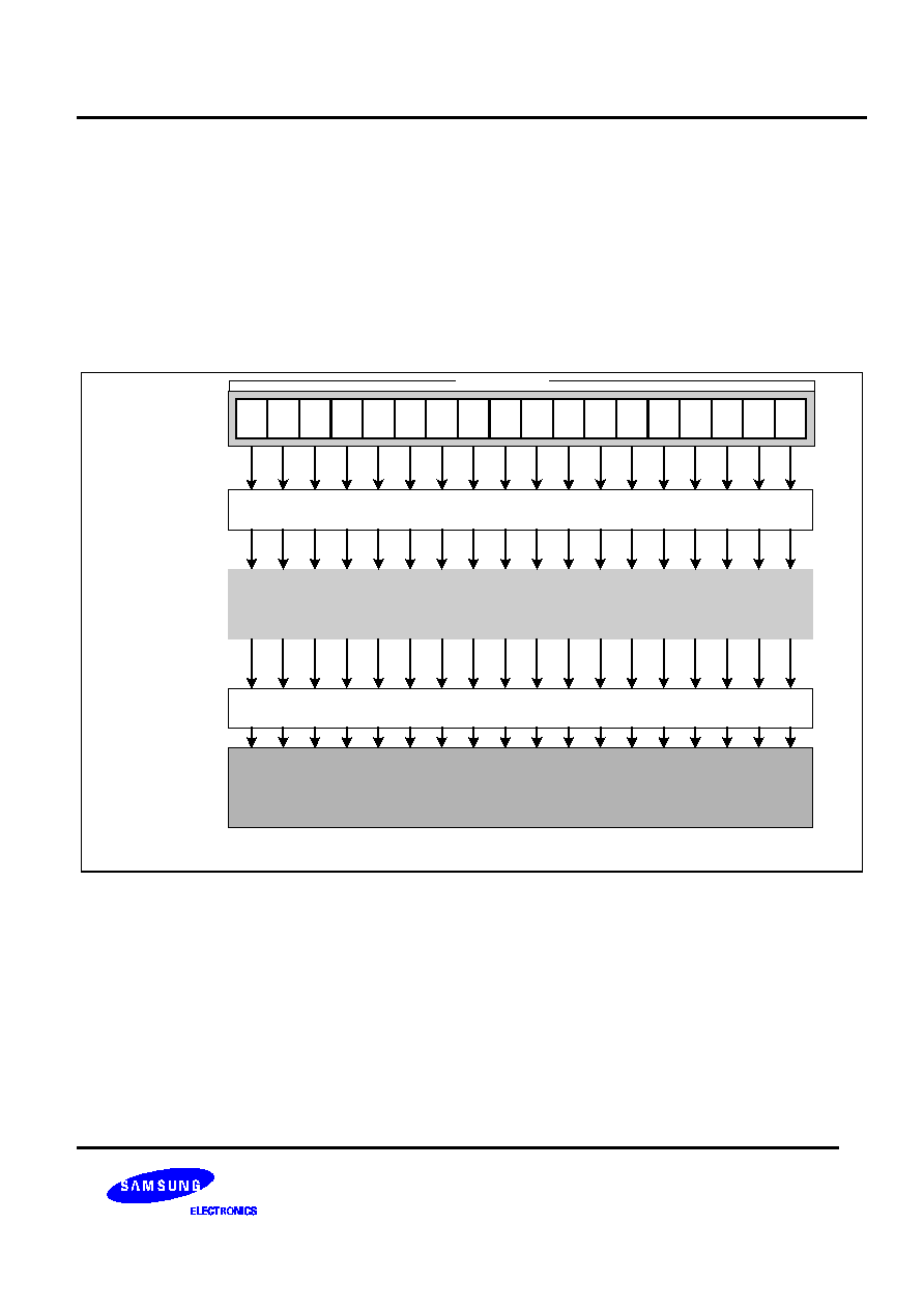
S6D0114 132-RGB X 176-DOT 1-CHIP DRIVER IC FOR 262,144-COLOR TFT-LCD DISPLAY
Preliminary
37
LG2�0: Compare the data read from the GRAM by the microcomputer with the compare registers (CP17�0) by a
compare/logical operation and write the results to GRAM. For details, see the Logical/Compare Operation Function.
CP17�0: Set the compare register for the compare operation with the data read from the GRAM or written by the
microcomputer.
Note: this function is not available when the external display interface (i.e. RGB interface or VSYNC interface) is in use.
Therefore, LG2-0 bits should be set to be "000", respectively.
DB
17
DB
16
DB
15
DB
14
DB
13
DB
12
DB
11
DB
10
DB
9
DB
8
DB
7
DB
6
DB
5
DB
4
DB
3
DB
2
DB
1
DB
0
Write Data to
GRAM *1
write data to
GRAM
Logical/
Compare
operation
18 bits
Conversion of RGB to BGR (vice versa)
Logic operation(write data)
Compare operation (with compare register)
LG2-0 = 000 : Replacement
LG2-0 = 110 : Replacement of matched write data
Write Data Mask (WM17-0)
GRAM
Figure 7. RGB swapping and Logical/compare operation
Note: 1) Data is written to GRAM in 18-bit units. Logical and compare operations are also performed in 18-bit units.
2) The write data mask(WM17-0) is set by the register in the RAM write data mask section
132-RGB X 176-DOT 1-CHIP DRIVER IC FOR 262,144-COLOR TFT-LCD DISPLAY
S6D0114
Preliminary
38
Display Control (R07h)
R/W
RS
DB15
DB14
DB13
DB12
DB11
DB10
DB9
DB8
DB7
DB6
DB5
DB4
DB3
DB2
DB1
DB0
W
1
0
0
0
PT1
PT0
VLE2
VLE1
SPT
0
0
GON
DTE
CL
REV
D1
D0
PT1-0: Normalize the source outputs when non-displayed area of the partial display is driven. For details, see the
Screen-division Driving Function section.
Source Output for Non-display Area
Gate Output for Non-display Area
PT1
PT0
Positive Polarity
Negative Polarity
Gate driver used
0
0
V63
V0
Normal Drive
0
1
V0
V63
Vgoff
1
0
GND
GND
Vgoff
1
1
Hi-z
Hi-z
Vgoff
VLE2�1: When VLE1 = 1, a vertical scroll is performed in the 1st screen. When VLE2 = 1, a vertical scroll is
performed in the 2nd screen. Vertical scrolling on the two screens cannot be controlled at the same time.
VLE2
VLE1
2
nd
Screen
1
st
Screen
0
0
Fixed display
Fixed display
0
1
Fixed display
Scroll
1
0
Scroll
Fixed display
1
1
Setting disabled
Setting disabled
SPT: When SPT = 1, the 2-division LCD drive is performed. For details, see the Screen-division Driving Function
section.
Note: this function is not available when the external display interface (i.e. RGB interface or VSYNC interface) is in use.
GON: Gate off level is set to be VSS when GON = 0.
When GON= 0 and DISPTMG= 0, G1 to G176 output is fixed to VSS level. When GON= 1, G1 to G176 output is
fixed to VGH or Vgoff level. See the instruction set up flow for further description on the display on/off flow.
DTE: DISPTMG output is fixed to VSS when DTE = 0.
GON
Gate output
DTE
DISPTMG output
0
VGH/VSS
0
Halt (VSS)
1
VGH/Vgoff
1
Operation (VDD/VSS)
CL: CL = 1 selects 8-color display mode. For details, see the section on 8-color display mode.
CL
Number of display colors
0
262,144 colors
1
8 colors
S6D0114 132-RGB X 176-DOT 1-CHIP DRIVER IC FOR 262,144-COLOR TFT-LCD DISPLAY
Preliminary
39
REV: Displays all character and graphics display sections with reversal when REV = 1. For details, see the
Reversed Display Function section. Since the grayscale level can be reversed, display of the same data is enabled
on normally white and normally black panels.
1) Combination with the PT1-0 bit
Source output level
Non-display area
Display Area
PT1-0=(0,0)
PT1-0=(0,1)
PT1-0=(1,0)
PT1-0=(1,1)
REV
GRAM
data
Positive
Negative
Positive
Negative
Positive
Negative
Positive
Negative
Positive
Negative
0
18'h00000
:
18'h3FFFF
V63
:
V0
V0
:
V63
V63
V0
V63
V0
VSS
VSS
Hi-z
Hi-z
1
18'h0000
:
18'h3FFFF
V0
:
V63
V63
:
V0
V63
V0
V63
V0
VSS
VSS
Hi-z
Hi-z
D1�0: Display is on when D1 = 1 and off when D1 = 0. When off, the display data remains in the GRAM, and can be
re-displayed instantly by setting D1 = 1. When D1 is 0, the display is off with the entire source outputs set to the VSS
level. Because of this, the S6D0114 can control the charging current for the LCD with AC driving. Control the display
on/off while control GON and DTE. For details, see the Instruction Set Up Flow.
When D1�0 = 01, the internal display of the S6D0114 is performed although the display is off. When D1-0 = 00, the
internal display operation halts and the display is off.
D1
D0
Source
output
S6D0114 internal
display operation
Master/slave signal
(CL1, FLM, M, DISPTMG)
0
0
VSS
Halt
Halt
0
1
VSS
Operate
Operate
1
0
Unlit display
Operate
Operate
1
1
Display
Operate
Operate
Notes:
1. Writing from MCU to GRAM is independent from D1�0.
2. In sleep and standby mode, D1�0 = 00. However, the register contents of D1�0 are not modified
.
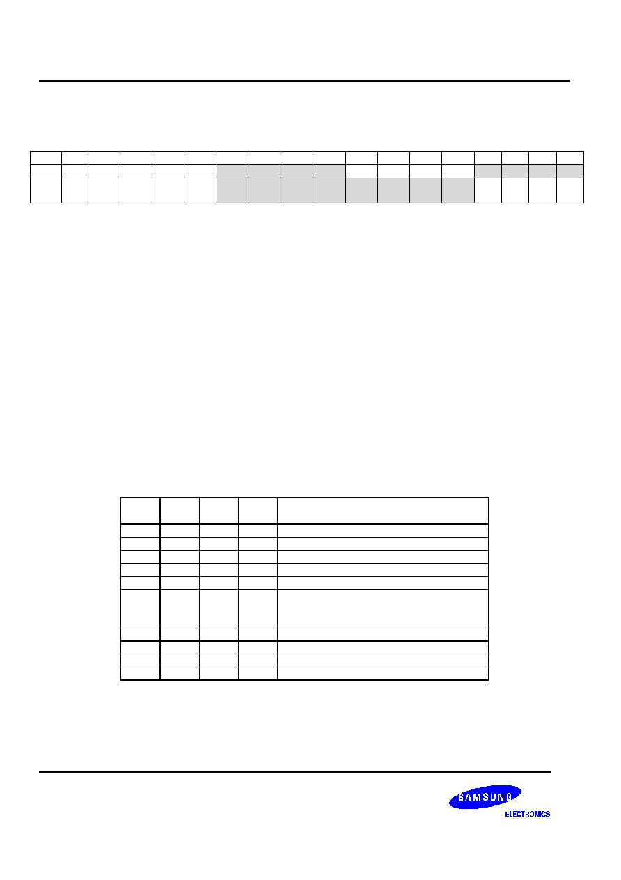
132-RGB X 176-DOT 1-CHIP DRIVER IC FOR 262,144-COLOR TFT-LCD DISPLAY
S6D0114
Preliminary
40
Blanking period control 1 (R08h)
Blanking period control 2 (R09h)
R/W
RS
DB15
DB14
DB13
DB12
DB11
DB10
DB9
DB8
DB7
DB6
DB5
DB4
DB3
DB2
DB1
DB0
W
1
0
0
0
0
FP3
FP2
FP1
FP0
0
0
0
0
BP3
BP2
BP1
BP0
W
1
0
0
0
0
BLP1
3
BLP1
2
BLP1
1
BLP1
0
BLP2
3
BLP2
2
BLP2
1
BLP2
0
0
0
0
0
The blanking period in the front and end of the display area can be defined using this register.
When N-raster-row is driving, a blank period is inserted after all screens are drawn. Front and Back porch can be
adjusted using FP3-0 and BP3-0 bits (R08h). In interlace drive mode, Blank period can be adjusted using BLP13-0
and BLP23-0 bit (R09h). For details, see the Graphics Operation Function section.
FP3-0/BP3-0: Set the periods of blanking (the front and back porch), which are placed at the beginning and end of
the display. FP3-0 are for a front porch and BP3-0 are for a back porch. When front and back porches are set, the
settings should meet the following conditions.
BP + FP = 16 raster-rows
FP
2 raster-rows
BP
2 raster-rows
When the external display interface is in use, the front porch (FP) will start on the falling edge of the VSYNC signal
and display operation commences at the end of the front-porch period. The back porch (BP) will start when data for
the number of raster-rows specified by the NL bits has been displayed. During the period between the completion of
the back-porch period and the next VSYNC signal, the display will remain blank.
NOTE: In the internal clock mode, the blanking periods described above should be BP=0011 (3 raster-rows) and FP=0101 (5 raster-rows)
Table 21. Front/Back Porch
FP3
BP3
FP2
BP2
FP1
BP1
FP0
BP0
# of Raster Periods In the Front Porch
# of Raster Periods In the Back Porch
0
0
0
0
Setting Disabled
0
0
0
1
Setting Disabled
0
0
1
0
2
0
0
1
1
3
0
1
0
0
4
.
.
.
.
.
.
.
.
.
.
.
.
.
.
.
1
1
0
0
12
1
1
0
1
13
1
1
1
0
14
1
1
1
1
Setting Disabled
BLP13-0/BLP23-0: In interlaced drive (3-field) mode, blanking period inserted every 1/3 frame. BLP13-0 and
BLP23-0 bit can/ adjust that blanking period.
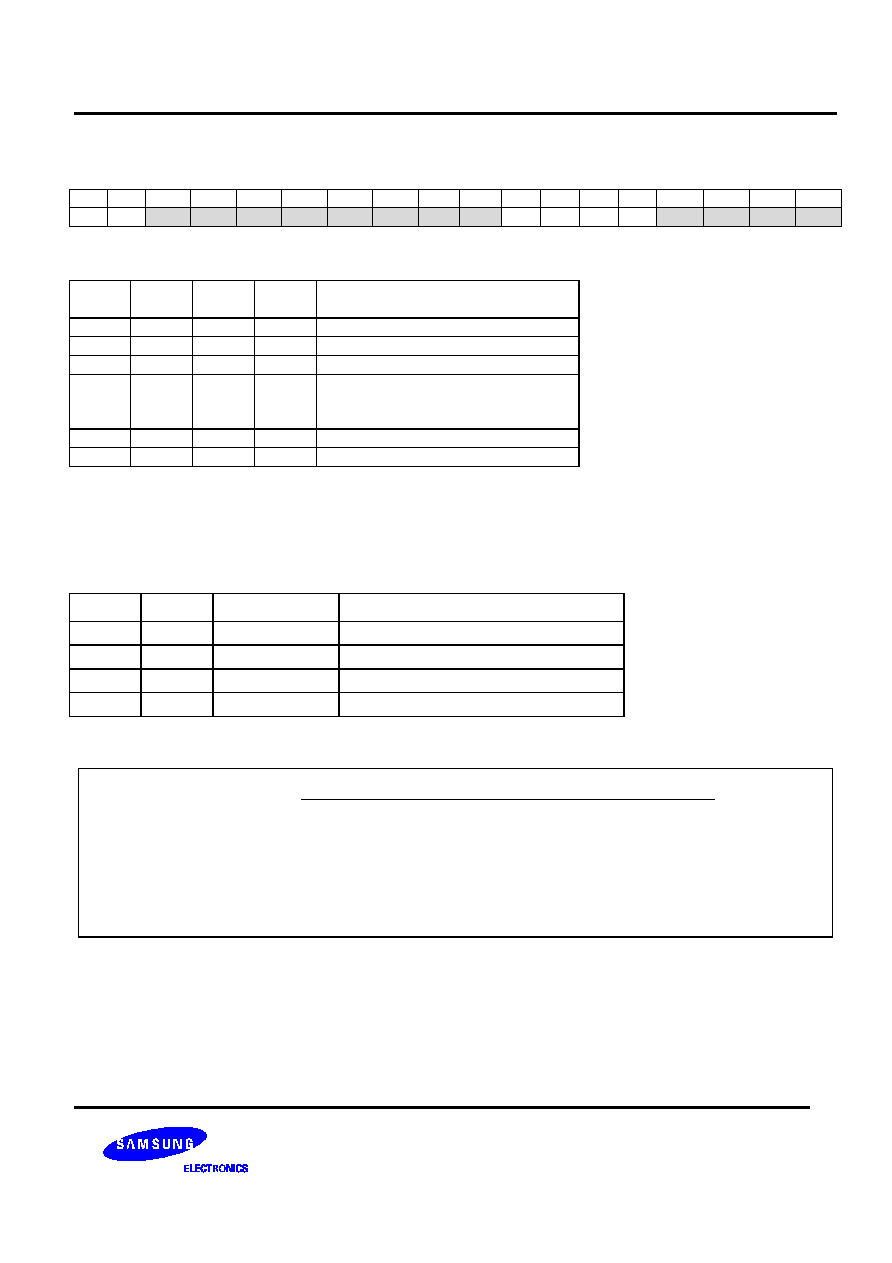
S6D0114 132-RGB X 176-DOT 1-CHIP DRIVER IC FOR 262,144-COLOR TFT-LCD DISPLAY
Preliminary
41
Frame Cycle Control (R0Bh)
R/W
RS
DB15
DB14
DB13
DB12
DB11
DB10
DB9
DB8
DB7
DB6
DB5
DB4
DB3
DB2
DB1
DB0
W
1
NO1
NO0
SDT1
SDT0
EQ1
EQ0
DIV1
DIV0
0
0
0
0
RTN3
RTN2
RTN1
RTN0
RTN3-0: Set the 1H period (1 raster-row).
RTN3
RTN2
RTN1
RTN0
Clock cycles per raster row
0
0
0
0
16
0
0
0
1
17
0
0
1
0
18
.
.
.
.
.
.
.
.
.
.
.
.
.
.
.
1
1
1
0
30
1
1
1
1
31
DIV1-0: Set the division ratio of clocks for internal operation (DIV1-0). Internal operations are driven by clocks, which
are frequency divided according to the DIV1-0 setting. Frame frequency can be adjusted along with the 1H period
(RTN3-0). When changing number of the drive cycle, adjust the frame frequency. For details, see the Frame
Frequency Adjustment Function section.
DIV1
DIV0
Division Ratio
Internal operation clock frequency
0
0
1
fosc/1
0
1
2
fosc/2
1
0
4
fosc/4
1
1
8
fosc/8
*fosc = R-C oscillation frequency
Frame Frequency =
f
OSC
Clock cycles per raster-row x division ratio x (Line+B)
[Hz]
f
OSC
: R-C oscillation frequency
Line: Number of raster-rows (NL bit)
Clock cycles per raster-row: RTN bit
Division ratio: DIV bit
B: Blank period(Back porch + Front Porch)
Figure 8. Formula for the frame frequency
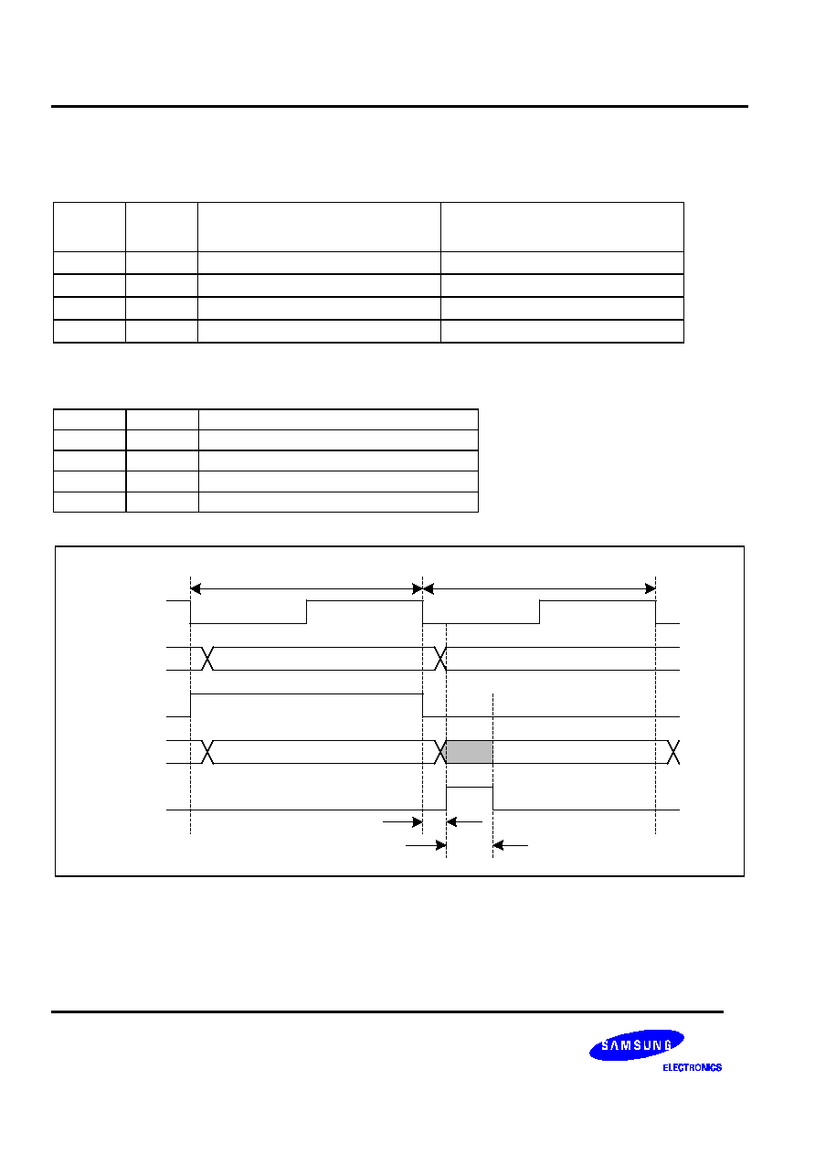
132-RGB X 176-DOT 1-CHIP DRIVER IC FOR 262,144-COLOR TFT-LCD DISPLAY
S6D0114
Preliminary
42
EQ1-0: EQ period is sustained for the number of clock cycle which is set on EQ1-0. When VcomL<0, set these bits
as "00" for preventing the abnormal function.
EQ1
EQ0
EQ period Internal Operation
(synchronized with internal clock)
RGB I/F Operation
(synchronized with DOTCLK)
0
0
No EQ
No EQ
0
1
1 clock cycle
8 clock cycle
1
0
2 clock cycle
16 clock cycle
1
1
3 clock cycle
24 clock cycle
SDT1-0: Set delay amount from gate edge (end) to source output.
SDT1
SDT0
Delay amount of the source output
0
0
1 clock cycle
0
1
2 clock cycle
1
0
3 clock cycle
1
1
4 clock cycle
CL1
M
Gn
Sn
EQ
1H period
1H period
Delay time for source output
Period of Equalizing
Figure 9. Set Delay from Gate Output to Source Output and EQ signal
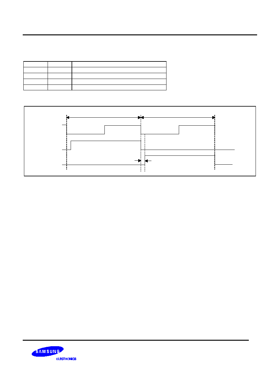
S6D0114 132-RGB X 176-DOT 1-CHIP DRIVER IC FOR 262,144-COLOR TFT-LCD DISPLAY
Preliminary
43
NO1-0: Set amount of non-overlay for the gate output.
NO1
NO0
Amount of non-overlap
0
0
0 clock cycle
0
1
4 clock cycle
1
0
6 clock cycle
1
1
8 clock cycle
Note: The amount of non-overlap time is defined from the falling edge of the CL1
Gn
Gn+1
1H period
1H period
Non-overlap period
CL1
Gn
Gn+1
1H period
1H period
Non-overlap period
CL1
Figure 10. Non-overlap Period
Note: The values specified by the bits of EQ, SDT1-0 and NO1-0 vary in a reference clock for each interface mode.
Internal operation mode: Internal R-C oscillation clock
RGB-I/F mode
: DOTCLK
VSYNC-I/F
: Internal R-C oscillation clock

132-RGB X 176-DOT 1-CHIP DRIVER IC FOR 262,144-COLOR TFT-LCD DISPLAY
S6D0114
Preliminary
44
External Display Control (R0Ch)
R/W
RS
DB15
DB14
DB13
DB12
DB11
DB10
DB9
DB8
DB7
DB6
DB5
DB4
DB3
DB2
DB1
DB0
W
1
0
0
0
0
0
0
0
RM
0
0
DM1
DM2
0
0
RIM1
RIM0
RIM1-0: Specify the RGB interface mode when the RGB interface is used. Specifically, this setting specifies the
mode when the bits of DM and RM are set to RGB interface. These bits should be set before display operation
through the RGB interface and should not be set during operation.
RIM1
RIM0
RGB Interface Mode
0
0
18-bit RGB interface (one transfer/pixel)
0
1
16-bit RGB interface (one transfer /pixel)
1
0
6-bit RGB interface (three transfers /pixel)
1
1
Setting disabled
DM1-0: Specify the display operation mode. The interface can be set based on the bits of DM1-0. This setting
enables switching interface between internal operation and the external display interface.
Switching between two external display interfaces (RGB interface and VSYNC interface) should not be done.
DM1
DM0
RGB Interface Mode
0
0
Internal clock operation
0
1
RGB interface
1
0
VSYNC interface
1
1
Setting disabled
RM: Specifies the interface for RAM accesses. RAM accesses can be performed through the interface specified by
the bits of RM1-0. When the display data is written via the RGB interface, 1 should be set. This bit and the DM bits
can be set independently. The display data can be written via the system interface by clearing this bit while the RGB
interface is used.
RM
Interface for RAM Access
0
System interface / VSYNC interface
1
RGB interface
S6D0114 132-RGB X 176-DOT 1-CHIP DRIVER IC FOR 262,144-COLOR TFT-LCD DISPLAY
Preliminary
45
Depending on the external display interface setting, differnet interfaces for use can be specified to match the display
state. While displaying moving pictures (RGB interface/VSYNC interface), the data for display can be written in
high-speed write mode, which achieves both low power consumption and high-speed access.
Table 22. Display State and Interface
Display State
Operation Mode
RAM Access (RM)
Display Operation Mode
(DM1-0)
Still Pictures
Internal Clock
System interface
(RM=0)
Internal clock
(DM1-0=00)
Motion Pictures
RGB interface (1)
RGB interface
(RM=1)
RGB interface
(DM1-0=01)
Rewrite still picture area while
displaying motion pictures
RGB interface (2)
System interface
(RM=0)
RGB interface
(DM1-0=01)
Motion Picture Display
VSYNC interface
System interface
(RM=0)
VSYNC interface
(DM1-0=10)
NOTE:
1) The instruction register can only be set through the system interface.
2) Switching between RGB interface and VSYNC interface cannot be done.
3) The RGB interface mode should not be set during operation.
4) For the transition flow for each operation mode, see the External Display Interface section.
5) RGB interface and VSYNC interface should be used in high-speed write mode (HWM=1).
Internal Clock Mode
All display operation is controlled by signals generated by the internal clock in internal clock mode.
All inputs through the external display interface are invalid. The internal RAM can be accessed only via the system
interface.
RGB Interface Mode (1)
The display operations are controlled by the frame synchronization clock (VSYNC), raster-row synchronization
signal (VSYNC), and dot clock (DCLK) in RGB interface mode. These signals should be supplied during display
operation in this mode.
The display data is transferred to the internal RAM via PD17-0 for each pixel. Combining the function of the high-
speed write mode and the window address enables display of both the motion picture area and the internal RAM
area simultaneously. In this method, data is only transferred when the screen is updated, which reduces the amount
of data transferred.
The periods of the front (FP), back (BP) porch, and the display are automatically generated in the S6D0114 by
counting the raster-row synchronization signal (HSYNC) based on the frame synchronization signal (VSYNC).
RGB Interface Mode (2)
When RGB interface is in use, data can be written to RAM via the system interface. This write operation should be
performed while data for display is not being transferred via RGB interface (ENABLE = low). Before the next data
transfer for display via RGB interface, the setting above should be changed, and then the address and index (R22h)
should be set.

132-RGB X 176-DOT 1-CHIP DRIVER IC FOR 262,144-COLOR TFT-LCD DISPLAY
S6D0114
Preliminary
46
VSYNC Interface Mode
The internal display operation is synchronized with the frame synchronization signal (VSYNC) in VSYNC interface
mode. When data is written to the internal RAM with the required speed after the falling edge of VSYNC, motion
pictures can be displayed via the conventional interface. There are some limitations on the timing and methods of
writing to RAM. See the section on the external display interface.
In VSYNC interface mode. Only the VSYNC input is valid. The other input signals for the external display interface
are invalid.
The periods of the front and back porch and display period are automatically generated by the frame
synchronization signal (VSYNC) according to the setting of the S6D0114 registers.
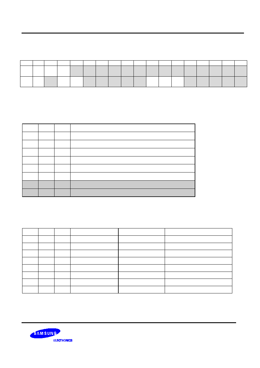
S6D0114 132-RGB X 176-DOT 1-CHIP DRIVER IC FOR 262,144-COLOR TFT-LCD DISPLAY
Preliminary
47
Power Control 1 (R10h)
Power Control 2 (R11h)
R/W
RS
DB15
DB14
DB13
DB12
DB11
DB10
DB9
DB8
DB7
DB6
DB5
DB4
DB3
DB2
DB1
DB0
W
1
0
0
SAP
2
SAP
1
SAP
0
BT2
BT1
BT0
DC2
DC1
DC0
AP2
AP1
AP0
SLP
STB
W
1
CAD
0
0
VRN
4
VRN
3
VRN
2
VRN
1
VRN
0
0
0
0
VRP
4
VRP
3
VRP
2
VRP
1
VRP
0
SAP2-0: Adjust the amount of fixed current from the fixed current source in the operational amplifier for the source
driver. When the amount of fixed current is large, LCD driving ability and the display quality become high, but the
current consumption is increased. Adjust the fixed current considering the display quality and the current
consumption. During non-display, when SAP2-0 = "000", the current consumption can be reduced by ending the
operational amplifier and step-up circuit operation.
SAP2 SAP1 SAP0
Amount of Current in Operational Amplifier
0
0
0
Operation of the operational amplifier and step-up circuit stops.
0
0
1
Small
0
1
0
Small or medium
0
1
1
Medium
1
0
0
Medium or large
1
0
1
Large
1
1
0
Setting disabled
1
1
1
Setting disabled
BT2�0: The output factor of step-up is switched. Adjust scale factor of the step-up circuit by the voltage used. When
the step-up operating frequency is high, the driving ability of the step-up circuit and the display quality become high,
but the current consumption is increased. Adjust the frequency considering the display quality and the current
consumption.
BT2
BT1
BT0
VLOUT1 Output
VLOUT2 Output
Notes*
0
0
0
2 X Vci1
3 X Vci2
VLOUT2 = Vci1 X six times
0
0
1
2 X Vci1
4 X Vci2
VLOUT2 = Vci1 X eight times
0
1
0
3 X Vci1
3 X Vci2
VLOUT2 = Vci1 X nine times
0
1
1
3 X Vci1
2 X Vci2
VLOUT2 = Vci1 X six times
1
0
0
2 X Vci1
Vci1 + 2 X Vci2
VLOUT2 = Vci1 X five times
1
0
1
2 X Vci1
Vci1 + 3 X Vci2
VLOUT2 = Vci1 X seven times
1
1
0
Step-up stopped
3 X Vci2
VLOUT2 = Vci2 X three times
1
1
1
Step-up stopped
4 X Vci2
VLOUT2 = Vci2 X four times
Note: The step-up factors of VLOUT2 are derived from Vci1 when VLOUT1 and Vci2 are shorted. The conditions of VLOUT1 5.5V and VLOUT2
15.0V must be satisfied.
132-RGB X 176-DOT 1-CHIP DRIVER IC FOR 262,144-COLOR TFT-LCD DISPLAY
S6D0114
Preliminary
48
DC2-0: The operating frequency in the step-up circuit is selected. When the step-up operating frequency is high, the
driving ability of the step-up circuit and the display quality become high, but the current consumption is increased.
Adjust the frequency considering the display quality and the current consumption.
DC2
DC1
DC0
Step-up Cycle in Step-up Circuit1
Step-up Cycle in Step-up Circuit 2/3/4
0
0
0
DCCLK / 1
DCCLK / 4
0
0
1
DCCLK / 2
DCCLK / 4
0
1
0
DCCLK / 4
DCCLK / 4
0
1
1
DCCLK / 2
DCCLK / 16
1
0
0
DCCLK
DCCLK / 8
1
0
1
DCCLK / 2
DCCLK / 8
1
1
0
DCCLK / 4
DCCLK / 8
1
1
1
DCCLK / 4
DCCLK / 16
AP2�0: The amount of fixed current in the operational amplifier for the power supply can be adjusted. When the
amount of fixed current is large, the LCD driving ability and the display quality become high, but the current
consumption is increased. Adjust the fixed current considering the display quality and the current consumption.
During no display, when AP2-0 = "000", the current consumption can be reduced by ending the operational amplifier
and step-up circuit operation.
AP2
AP1
AP0
Amount of Current in Operational Amplifier
0
0
0
Operation of the operational amplifier and step-up circuit
stops.
0
0
1
Small
0
1
0
Small or medium
0
1
1
Medium
1
0
0
Medium or large
1
0
1
Large
1
1
0
Setting Inhibited
1
1
1
Setting Inhibited
SLP: When SLP = 1, the S6D0114 enters the sleep mode, where the internal display operations are halted except
for the R-C oscillator, thus reducing current consumption. Only the following instructions can be executed during the
sleep mode.
-
Power control (BT2�0, DC3�0, AP2�0, SLP, STB, VC2-0, CAD, VR3-0, VRL3-0, VRH4-0, VCOMG,
VDV4-0, and VCM4-0 bits)
During the sleep mode, the other GRAM data and instructions cannot be updated although they are retained and G1
to G176 output is fixed to VSS level, and register set-up is protected (maintained).

S6D0114 132-RGB X 176-DOT 1-CHIP DRIVER IC FOR 262,144-COLOR TFT-LCD DISPLAY
Preliminary
49
STB: When STB = 1, the S6D0114 enters the standby mode, where display operation completely stops, halting all
the internal operations including the internal R-C oscillator. Further, no external clock pulses are supplied. For
details, see the Standby Mode section. Only the following instructions can be executed during the standby mode.
-
Standby mode cancel(STB = "0")
-
Start oscillation
CAD: Set this bit according to the structure for the TFT-display retention volume.
CAD = 0: Set this bit when the Cst retention volume is structured. In this case, Vgoff level is fixed to VgoffL level
regardless of the Vcom alternating drive.
CAD = 1: Set this bit when the Cadd retention volume is structured. At the Vcom alternating drive, the Vgoff voltage
is output in the VgoffL voltage reference by the amount of Vcom alternating amplitude.
VRP4-0: Control oscillation (positive polarity) of 64-grayscale. For details, see the Oscillation Adjusting Circuit
section.
VRN4-0: Control oscillation (negative polarity) of 64-grayscale. For details, see the Oscillation Adjusting Circuit
section.
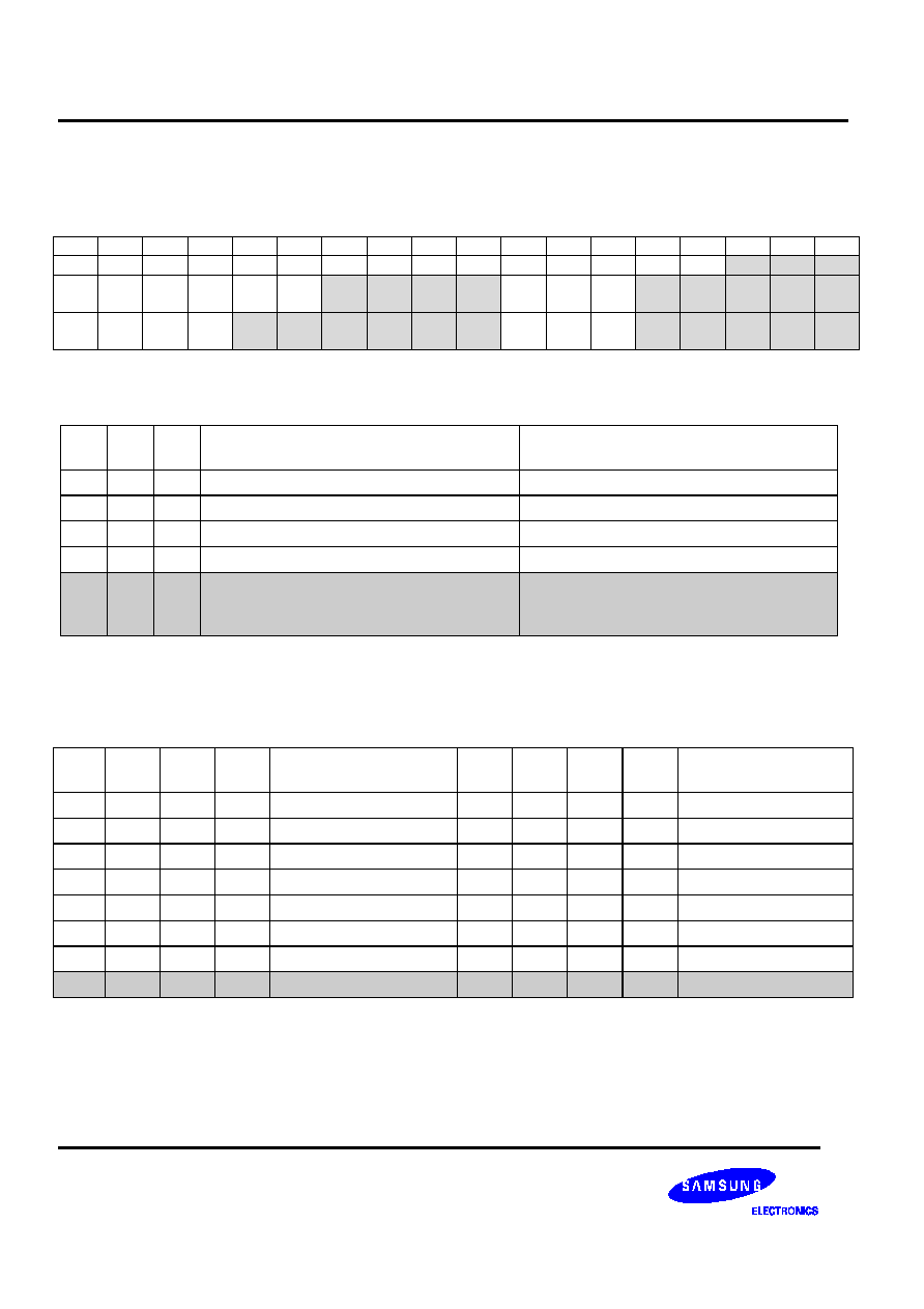
132-RGB X 176-DOT 1-CHIP DRIVER IC FOR 262,144-COLOR TFT-LCD DISPLAY
S6D0114
Preliminary
50
Power Control 3 (R12h)
Power Control 4 (R13h)
Power Control 5 (R14h)
R/W
RS
DB15
DB14
DB13
DB12
DB11
DB10
DB9
DB8
DB7
DB6
DB5
DB4
DB3
DB2
DB1
DB0
W
1
0
0
0
0
0
0
0
0
0
0
0
0
0
VC2
VC1
Vc0
W
1
0
0
0
0
VRL
3
VRL
2
VRL
1
VRL
0
0
0
0
PON
VRH
3
VRH
2
VRH
1
VRH
0
W
1
0
0
VCO
MG
VDV
4
VDV
3
VDV
2
VDV
1
VDV
0
0
0
0
VCM
4
VCM
3
VCM
2
VCM
1
VCM
0
VC2-0: Adjust reference voltage of VREG1, VREG2OUT and Vciout to optional rate of Vci. Also, when VC2 = "1", it
is possible to stop the internal reference voltage generator. This leads to optional power on for VREG1OUT/Vciout
with REGP and VREG2OUT with REGN externally.
VC2 VC1 VC0
Internal Reference Voltage (REGP) of
VREG1OUT and Vciout
Internal Reference Voltage (REGN) of
VREG2OUT
0
0
0
0.92 X Vci
0.08 X Vci
0
0
1
0.83 X Vci
0.17 X Vci
0
1
0
0.73 X Vci
0.27 X Vci
0
1
1
0.68 X Vci
0.32 X Vci
1
*
*
Stops generation of the internal reference
voltages of VREG1OUT and Vciout (REGP
can be input externally)
Stops generation of the internal reference
voltage of VREG2OUT (REGN can be input
externally).
Note: Leave these settings open because the voltage other than that for halting the internal circuit is output for REGP and REGN
.
VRL3- 0: Set magnification of amplification for VREG2OUT voltage (voltage for the reference voltage, VREG2 while
generating Vgoffout.) It allows magnifying the amplification of REGN from 2 to 8.5 times.
VRL
3
VRL
2
VRL
1
VRL
0
VREG2OUT Voltage
VRL
3
VRL
2
VRL
1
VRL
0
VREG2OUT Voltage
0
0
0
0
-(Vci � REGN) X 3.0
1
0
0
0
-(Vci � REGN) X 6.5
0
0
0
1
-(Vci � REGN) X 3.5
1
0
0
1
-(Vci � REGN) X 7.0
0
0
1
0
-(Vci � REGN) X 4.0
1
0
1
1
-(Vci � REGN) X 7.5
0
0
1
1
-(Vci � REGN) X 4.5
1
0
1
0
-(Vci � REGN) X 8.0
0
1
0
0
-(Vci � REGN) X 5.0
1
1
0
1
-(Vci � REGN) X 8.5
0
1
0
1
-(Vci � REGN) X 5.5
1
1
0
0
-(Vci � REGN) X 9.0
0
1
1
0
-(Vci � REGN) X 6.0
1
1
1
0
-(Vci � REGN) X 9.5
0
1
1
1
Stopped
1
1
1
1
Stopped
Note:
1) These settings apply when the internal reference-voltage generation circuit is stopped and the VREG2OUT voltage is
generated specifying REGN as the reference voltage.
2) Adjust the settings between the voltage set by (Vci � VC2-0) or the (Vci � REGN) voltage and VRL0 to VRL3 so that the
VREG2OUT voltage is higher than �16.0 V.
3) The VREG2OUT voltage is the factor when Vci is the reference voltage.
S6D0114 132-RGB X 176-DOT 1-CHIP DRIVER IC FOR 262,144-COLOR TFT-LCD DISPLAY
Preliminary
51
PON: This is an operation-starting bit for the booster circuit 4. PON = 0 is to stop and PON = 1 to start operation. For
further information about timing for adjusting to the PON = 1, please refer to the set up flow of power supply circuit.
VRH3-0: Set the amplified factor of the VREG1OUT voltage (the voltage for the reference voltage, VREG2 while
generating VgoffOUT). It allows to amplify from 1.45 to 2.85 times of REGN input voltage.
VRH
3
VRH
2
VRH
1
VRH
0
VREG1OUT Voltage
VRH
3
VRH
2
VRH
1
VRH
0
VREG1OUT Voltage
0
0
0
0
REGP X 1.45 times
1
0
0
0
REGP X 2.175 times
0
0
0
1
REGP X 1.55 times
1
0
0
1
REGP X 2.325 times
0
0
1
0
REGP X 1.65 times
1
0
1
1
REGP X 2.475 times
0
0
1
1
REGP X 1.75 times
1
0
1
0
REGP X 2.625 times
0
1
0
0
REGP X 1.80 times
1
1
0
1
REGP X 2.700 times
0
1
0
1
REGP X 1.85 times
1
1
0
0
REGP X 2.775 times
0
1
1
0
REGP X 1.90 times
1
1
1
0
REGP X 2.850 times
0
1
1
1
Stopped
1
1
1
1
Stopped
Note:
1) These settings apply when the internal reference-voltage generation circuit is stopped and the VREG1OUT voltage is generated
specifying REGP as the reference voltage.
2) Adjust the settings between the voltage set by VC2-0 or the REGP voltage and VRH0 to VRH3 so that the VREG1OUT voltage is
lower than 5.0 V.
VCOMG: When VCOMG = 1, VcomL voltage can output to negative voltage (-5V).
When VCOMG = 0, VcomL voltage becomes VSS and stops the amplifier of the negative voltage. Therefore, low
power consumption is accomplished. Also, When VCOMG = 0 and when Vcom is driven in A/C, set up of the
VDV4-0 is invalid. In this case, adjustment of Vcom/Vgoff A/C oscillation must be adjusted VcomH with VCM4-0.
VDV4-0: Set the alternating amplitudes of Vcom and Vgoff at the Vcom alternating drive. These bits amplify Vcom
and Vgoff 0.6 to 1.23 times the VREG1 voltage. When the Vcom alternation is not driven, the settings become
invalid.
VDV
4
VDV
3
VDV
2
VDV
1
VDV
0
Vcom
Amplitude
VDV
4
VDV
3
VDV
2
VDV
1
VDV
0
Vcom
Amplitude
0
0
0
0
0
VREG1 X 0.60
1
0
0
0
1
VREG1 X 1.08
0
0
0
0
1
VREG1 X 0.63
1
0
0
1
0
VREG1 X 1.11
0
0
0
1
0
VREG1 X 0.66
1
0
0
1
1
VREG1 X 1.14
:
:
:
:
:
:
1
0
1
0
0
VREG1 X 1.17
0
1
1
0
0
VREG1 X 0.96
1
0
1
0
1
VREG1 X 1.20
0
1
1
0
1
VREG1 X 0.99
1
0
1
1
0
VREG1 X 1.23
0
1
1
1
0
VREG1 X 1.02
1
0
1
1
1
Setting disabled
0
1
1
1
1
Setting disabled
1
1
*
*
*
Setting disabled
1
0
0
0
0
VREG1 X 1.05
Note: Adjust the settings between VREG1 and VDV0 to VDV4 so that the Vcom and Vgoff amplitudes are lower than 6.0 V.
132-RGB X 176-DOT 1-CHIP DRIVER IC FOR 262,144-COLOR TFT-LCD DISPLAY
S6D0114
Preliminary
52
VCM4-0: Set the VcomH voltage (a high-level voltage at the Vcom alternating drive). These bits amplify the VcomH
voltage 0.4 to 0.98 times the VREG1 voltage. When VCOM4-0 = 1, the adjustment of the internal volume stops, and
VcomH can be adjusted from VcomR by an external resistor.
VCM4
VCM3
VCM2
VCM1
VCM0
VcomH Voltage
0
0
0
0
0
VREG1 X 0.40 times
0
0
0
0
1
VREG1 X 0.42 times
0
0
0
1
0
VREG1 X 0.44 times
: : : : : :
0
1
1
0
0
VREG1 X 0.64 times
0
1
1
0
1
VREG1 X 0.66 times
0
1
1
1
0
VREG1 X 0.68 times
0
1
1
1
1
The internal volume stops and VcomH can be adjusted
from VcomR by an external variable resistor.
1
0
0
0
0
VREG1 X 0.70 times
1
0
0
0
1
VREG1 X 0.72 times
1
0
0
1
0
VREG1 X 0.74 times
: : : : : :
1
1
1
0
0
VREG1 X 0.94 times
1
1
1
0
1
VREG1 X 0.96 times
1
1
1
1
0
VREG1 X 0.98 times
1
1
1
1
1
The internal volume stops, and VcomH can be
adjusted from VcomR by an external variable resistor.
Note: Adjust the settings between VREG1 and VCM0 to VCM4 so that the VcomH voltage is lower than GVDD.
S6D0114 132-RGB X 176-DOT 1-CHIP DRIVER IC FOR 262,144-COLOR TFT-LCD DISPLAY
Preliminary
53
RAM Address Set (R21h)
R/W
RS
DB15
DB14
DB13
DB12
DB11
DB10
DB9
DB8
DB7
DB6
DB5
DB4
DB3
DB2
DB1
DB0
W
1
AD15
AD14
AD13
AD12
AD11
AD10
AD9
AD8
AD7
AD6
AD5
AD4
AD3
AD2
AD1
AD0
AD15�0: Initially set GRAM addresses to the address counter (AC). Once the GRAM data is written, the AC is
automatically updated according to the AM and I/D bit settings. This allows consecutive accesses without resetting
address. Once the GRAM data is read, the AC is not automatically updated. GRAM address setting is not allowed in
the standby mode. Ensure that the address is set within the specified window address
When RGB interface is in use (RM=1), AD15-0 will be set at the falling edge of the VSYNC signal.
When the internal clock operation and VSYNC interface (RM=1) are in use, AD15-0 will be set upon execution of an
instruction.
AD15 to AD0
GRAM setting
"0000H" to "0083"H
Bitmap data for G1
"0100H" to "0183"H
Bitmap data for G2
"0200H" to "0283"H
Bitmap data for G3
"0300H" to "0383"H
Bitmap data for G4
:
:
:
:
:
:
"AC00H" to "AC83"H
Bitmap data for G173
"AD00H" to "AD83"H
Bitmap data for G174
"AE00H" to "AE83"H
Bitmap data for G175
"AF00H" to "AF83"H
Bitmap data for G176
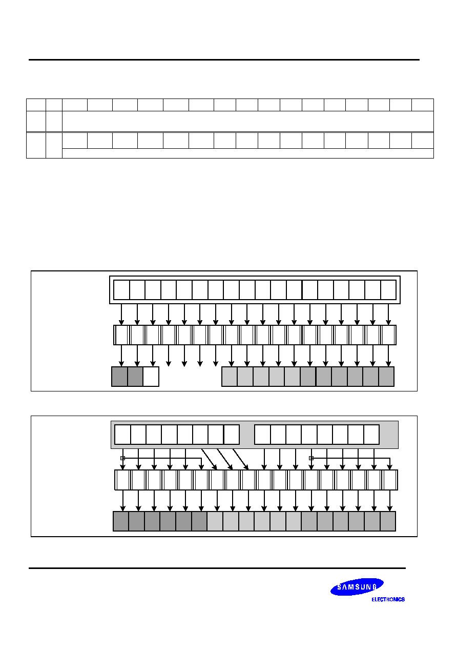
132-RGB X 176-DOT 1-CHIP DRIVER IC FOR 262,144-COLOR TFT-LCD DISPLAY
S6D0114
Preliminary
54
Write Data to Gram (R22h)
R/W
RS
DB15
DB14
DB13
DB12
DB11
DB10
DB9
DB8
DB7
DB6
DB5
DB4
DB3
DB2
DB1
DB0
W
1
RAM write data (WD17-0): Pin assignment varies according to the interface method. (see the following figure for more information)
WD15
WD14
WD13
WD12
WD11
WD10
WD9
WD8
WD7
WD6
WD5
WD4
WD3
WD2
WD1
WD0
W
1
When RGB-interface
WD17-0: Input data for GRAM can be expanded to 18 bits. The expansion format varies according to the interface
method. The input data selects the grayscale level. After a write, the address is automatically updated according to
AM and I/D bit settings. The GRAM cannot be accessed in standby mode. When 16- or 8-bit interface is in use, the
write data is expanded to 18 bits by writing the MSB of the <R><B> data to its LSB.
When data is written to RAM used by RGB interface via the system interface, please make sure that write data
conflicts do not occur.
When the 18-bit RGB interface is in use, 18-bit data is written to RAM via PD17-0 and 262,144-colors are available.
When the 16-bit RGB interface is in use, the MSB is written to its LSB and 65,536-colors are available
INPUT DATA
R5
R4
R3
R2
R1
R0
G5
G4
G3
G2
G1
G0
B5
B4
B3
B2
B1
B0
RGB Arrangement
WD
17
WD
16
WD
15
WD
14
WD
13
WD
12
WD
11
WD
10
WD
9
WD
8
WD
7
WD
6
WD
5
WD
4
WD
3
WD
2
WD
1
WD
0
Write to GRAM
DB
17
DB
16
DB
15
DB
14
DB
13
DB
12
DB
11
DB
10
DB
9
DB
8
DB
7
DB
6
DB
5
DB
4
DB
3
DB
2
DB
1
DB
0
Figure 11. 18-bit System interface (260K-color)
INPUT DATA
R5
R4
R3
R2
R1
R0
G5
G4
G3
G2
G1
G0
B5
B4
B3
B2
B1
B0
RGB Arrangement
WD
17
WD
16
WD
15
WD
14
WD
13
WD
12
WD
11
WD
10
WD
9
WD
8
WD
7
WD
6
WD
5
WD
4
WD
3
WD
2
WD
1
WD
0
Write to GRAM
DB
17
DB
16
DB
15
DB
14
DB
13
DB
12
DB
11
DB
10
DB
8
DB
7
DB
6
DB
5
DB
4
DB
3
DB
2
DB
1
Figure 12. 16-bit System interface (65K-color)
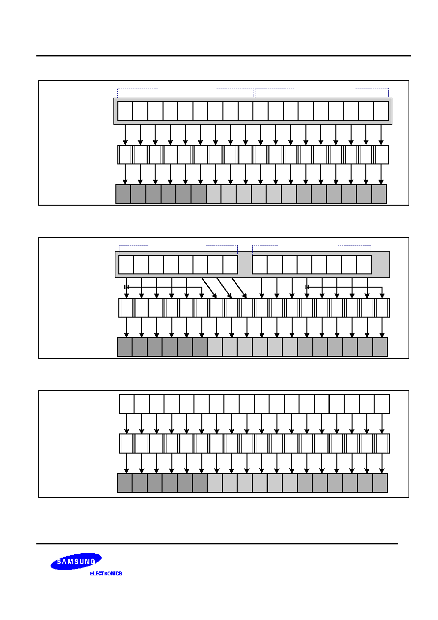
S6D0114 132-RGB X 176-DOT 1-CHIP DRIVER IC FOR 262,144-COLOR TFT-LCD DISPLAY
Preliminary
55
INPUT DATA
R5
R4
R3
R2
R1
R0
G5
G4
G3
G2
G1
G0
B5
B4
B3
B2
B1
B0
RGB Arrangement
WD
17
WD
16
WD
15
WD
14
WD
13
WD
12
WD
11
WD
10
WD
9
WD
8
WD
7
WD
6
WD
5
WD
4
WD
3
WD
2
WD
1
WD
0
Write to GRAM
DB
17
DB
16
DB
15
DB
14
DB
13
DB
12
DB
11
DB
10
DB
9
1st Transmission
DB
8
DB
7
DB
6
DB
5
DB
4
DB
3
DB
2
DB
1
DB
0
2nd Transmission
Figure 13. 9-bit System interface (260K-color)
INPUT DATA
R5
R4
R3
R2
R1
R0
G5
G4
G3
G2
G1
G0
B5
B4
B3
B2
B1
B0
RGB Arrangement
WD
17
WD
16
WD
15
WD
14
WD
13
WD
12
WD
11
WD
10
WD
9
WD
8
WD
7
WD
6
WD
5
WD
4
WD
3
WD
2
WD
1
WD
0
Write to GRAM
DB
17
DB
16
DB
15
DB
14
DB
13
DB
12
DB
11
DB
10
DB
8
DB
7
DB
6
DB
5
DB
4
DB
3
DB
2
DB
1
1st Transmission
2nd Transmission
Figure 14. 8-bit System interface (65K-color)
INPUT DATA
RGB Arrangement
WD
17
WD
16
WD
15
WD
14
WD
13
WD
12
WD
11
WD
10
WD
9
WD
8
WD
7
WD
6
WD
5
WD
4
WD
3
WD
2
WD
1
WD
0
Write to GRAM
R5
R4
R3
R2
R1
R0
G5
G4
G3
G2
G1
G0
B5
B4
B3
B2
B1
B0
PD
17
PD
16
PD
15
PD
14
PD
13
PD
12
PD
11
PD
10
PD
9
PD
8
PD
7
PD
6
PD
5
PD
4
PD
3
PD
2
PD
1
PD
0
Figure 15. 18-bit RGB interface (260K-color)
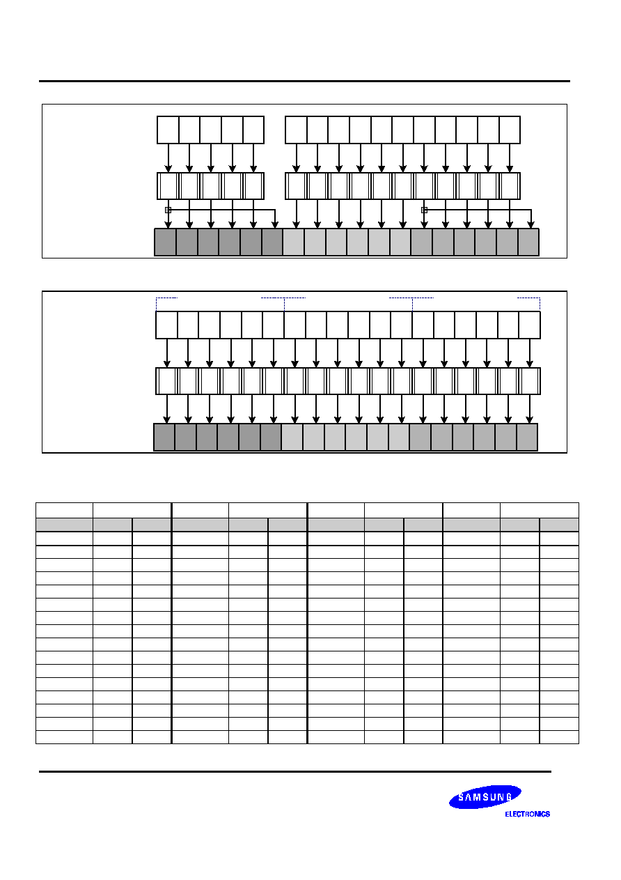
132-RGB X 176-DOT 1-CHIP DRIVER IC FOR 262,144-COLOR TFT-LCD DISPLAY
S6D0114
Preliminary
56
INPUT DATA
RGB Arrangement
WD
17
WD
16
WD
15
WD
14
WD
13
WD
11
WD
10
WD
9
WD
8
WD
7
WD
6
WD
5
WD
4
WD
3
WD
2
WD
1
Write to GRAM
R5
R4
R3
R2
R1
R0
G5
G4
G3
G2
G1
G0
B5
B4
B3
B2
B1
B0
PD
17
PD
16
PD
15
PD
14
PD
13
PD
11
PD
10
PD
9
PD
8
PD
7
PD
6
PD
5
PD
4
PD
3
PD
2
PD
1
Figure 16. 16-bit RGB interface (65K-color)
INPUT DATA
RGB Arrangement
WD
17
WD
16
WD
15
WD
14
WD
13
WD
12
WD
11
WD
10
WD
9
WD
8
WD
7
WD
6
WD
5
WD
4
WD
3
WD
2
WD
1
WD
0
Write to GRAM
R5
R4
R3
R2
R1
R0
G5
G4
G3
G2
G1
G0
B5
B4
B3
B2
B1
B0
PD
17
PD
16
PD
15
PD
14
PD
13
PD
12
PD
11
PD
10
PD
9
PD
8
PD
7
PD
6
PD
5
PD
4
PD
3
PD
2
PD
1
PD
0
1st Transmission
2nd Transmission
3rd Transmission
Figure 17. 6-bit RGB interface (260K-color)
Table 23. GRAM Data and Grayscale Level
GRAM data
Grayscale Polarity
GRAM Data
Grayscale Polarity
GRAM Data
Grayscale Polarity
GRAM Data
Grayscale Polarity
RGB
N
P
RGB
N
P
RGB
N
P
RGB
N
P
000000
V0
V63
010000
V16
V47
100000
V32
V31
110000
V48
V15
000001
V1
V62
010001
V17
V46
100001
V33
V30
110001
V49
V14
000010
V2
V61
010010
V18
V45
100010
V34
V29
110010
V50
V13
000011
V3
V60
010011
V19
V44
100011
V35
V28
110011
V51
V12
000100
V4
V59
010100
V20
V43
100100
V36
V27
110100
V52
V11
000101
V5
V58
010101
V21
V42
100101
V37
V26
110101
V53
V10
000110
V6
V57
010110
V22
V41
100110
V38
V25
110110
V54
V9
000110
V7
V56
010110
V23
V40
100110
V39
V24
110110
V55
V8
001000
V8
V55
011000
V24
V39
101000
V40
V23
111000
V56
V7
001001
V9
V54
011001
V25
V38
101001
V41
V22
111001
V57
V6
001010
V10
V53
011010
V26
V37
101010
V42
V21
111010
V58
V5
001011
V11
V52
011011
V27
V36
101011
V43
V20
111011
V59
V4
001100
V12
V51
011000
V28
V35
101100
V44
V19
111100
V60
V3
001101
V13
V50
011001
V29
V34
101101
V45
V18
111101
V61
V2
001100
V14
V49
011010
V30
V33
101100
V46
V17
111110
V62
V1
001101
V15
V48
011011
V31
V32
101101
V47
V16
111111
V63
V0
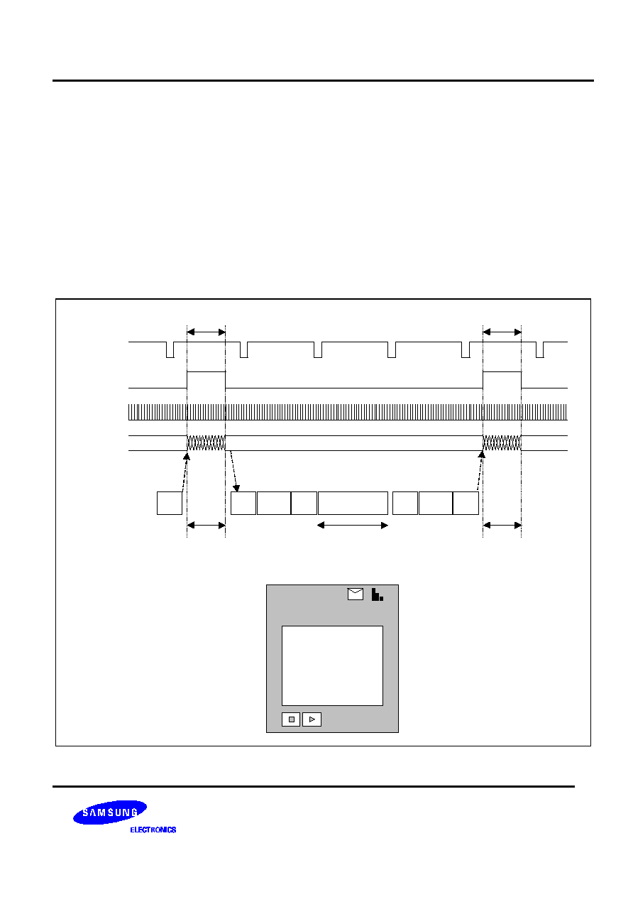
S6D0114 132-RGB X 176-DOT 1-CHIP DRIVER IC FOR 262,144-COLOR TFT-LCD DISPLAY
Preliminary
57
RAM ACCESS via RGB INTERFACE & SYSTEM INTERFACE
All the data for display is written to the internal RAM in the S6D0114 when RGB interface is in use. In this method,
data, including that in both the motion picture area and the screen update frame, can only be transferred via RGB
interface. In addition to using the high-speed write mode (HWM = 1) and the window address function, the power
consumption can be reduced and high-speed access can be achieved while motion pictures are being displayed.
Data for display that is not in the motion picture area or the screen update frame can be written via the system
interface.
RAM can be accessed via the system interface when RGB interface is in use. When data is written to RAM during
RGB interface mode, the ENABLE bit should be low to stop data writing via RGB interface, because RAM writing is
always performed in synchronization with the DOTCLK input when ENABLE is high. After this RAM access via the
system interface, a waiting time is needed for a write/read bus cycle before the next RAM access starts via RGB
interface. When a RAM write conflict occurs, data writing is not guaranteed.
VSYNC
ENABLE
DOTCLK
PD17-0
Serial
interface
RM=0
Index
R22
Address
set
Index
R22
Writing display data
except moving picture
display area
RM=0
Address
set
Index
R22
Moving picture
display area
2001/01/01 00:00
Still picture display area
Writing moving picture
display area
Writing moving picture
display area
Index set
Writing picture
Writing picture
Writing still picture
display area
Figure 18. RAM access via RGB Interface & System Interface

132-RGB X 176-DOT 1-CHIP DRIVER IC FOR 262,144-COLOR TFT-LCD DISPLAY
S6D0114
Preliminary
58
Read Data from GRAM (R22h)
R/W
RS
DB15
DB14
DB13
DB12
DB11
DB10
DB9
DB8
DB7
DB6
DB5
DB4
DB3
DB2
DB1
DB0
R
1
RAM Read data (RD17-0): Pin assignment varies according to the interface method. (see the following figure for more information)
RD17�0: Read 18-bit data from the GRAM. When the data is read to the MCU, the first-word read immediately after
the GRAM address setting is latched from the GRAM to the internal read-data latch. The data on the data bus
(DB15�0) becomes invalid and the second-word read is normal.
When bit processing, such as a logical operation, is performed within the S6D0114, only one read can be processed
since the latched data in the first word is used.
In case of 16-/8-bit interface, the LSB of <R><B> color data will not be read.
This function is not available in RGB interface mode.
OUPUT DATA
R5
R4
R3
R2
R1
R0
G5
G4
G3
G2
G1
G0
B5
B4
B3
B2
B1
B0
GRAM DATA
READ DATA
DB
17
DB
16
DB
15
DB
14
DB
13
DB
12
DB
11
DB
10
DB
9
DB
8
DB
7
DB
6
DB
5
DB
4
DB
3
DB
2
DB
1
DB
0
RD
17
RD
16
RD
15
RD
14
RD
13
RD
12
RD
11
RD
10
RD
9
RD
8
RD
7
RD
6
RD
5
RD
4
RD
3
RD
2
RD
1
RD
0
Figure 19. 18-bit System Interface for GRAM read
R5
R4
R3
R2
R1
R0
G5
G4
G3
G2
G1
G0
B5
B4
B3
B2
B1
B0
DB
17
DB
16
DB
15
DB
14
DB
13
DB
12
DB
11
DB
10
DB
8
DB
7
DB
6
DB
5
DB
4
DB
3
DB
2
DB
1
RD
17
RD
16
RD
15
RD
14
RD
13
RD
12
RD
11
RD
10
RD
9
RD
8
RD
7
RD
6
RD
5
RD
4
RD
3
RD
2
RD
1
RD
0
OUPUT DATA
GRAM DATA
READ DATA
Figure 20. 16-bit System Interface for GRAM read
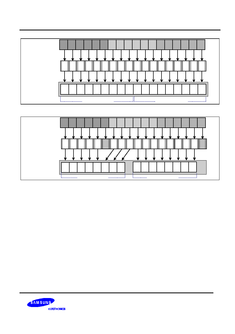
S6D0114 132-RGB X 176-DOT 1-CHIP DRIVER IC FOR 262,144-COLOR TFT-LCD DISPLAY
Preliminary
59
R5
R4
R3
R2
R1
R0
G5
G4
G3
G2
G1
G0
B5
B4
B3
B2
B1
B0
DB
17
DB
16
DB
15
DB
14
DB
13
DB
12
DB
11
DB
10
DB
9
1st Transmission
2nd Transmission
OUPUT DATA
GRAM DATA
READ DATA
RD
17
RD
16
RD
15
RD
14
RD
13
RD
12
RD
11
RD
10
RD
9
RD
8
RD
7
RD
6
RD
5
RD
4
RD
3
RD
2
RD
1
RD
0
DB
17
DB
16
DB
15
DB
14
DB
13
DB
12
DB
11
DB
10
DB
9
Figure 21. 9-bit System Interface for GRAM read
R5
R4
R3
R2
R1
R0
G5
G4
G3
G2
G1
G0
B5
B4
B3
B2
B1
B0
DB
17
DB
16
DB
15
DB
14
DB
13
DB
12
DB
11
DB
10
1st Transmission
2nd Transmission
OUPUT DATA
GRAM DATA
READ DATA
RD
17
RD
16
RD
15
RD
14
RD
13
RD
12
RD
11
RD
10
RD
9
RD
8
RD
7
RD
6
RD
5
RD
4
RD
3
RD
2
RD
1
RD
0
DB
17
DB
16
DB
15
DB
14
DB
13
DB
12
DB
11
DB
10
Figure 22. 8-bit System Interface for GRAM read

132-RGB X 176-DOT 1-CHIP DRIVER IC FOR 262,144-COLOR TFT-LCD DISPLAY
S6D0114
Preliminary
60
Sets the I/D, AM, HAS/HSE,
and VSA/VEA bits
Address: N set
Dummy read (invalid data)
GRAM -> Read data latch
Read (data of address N)
Read-data latch -> DB17-0
Address: M set
Dummy read (invalid data)
GRAM -> Read data latch
Read (data of address M)
Read-data latch -> DB17-0
Sets the I/D, AM, HAS/HSE,
and VSA/VEA bits
Address: N set
Dummy read (invalid data)
GRAM -> Read data latch
Write (data of address N)
DB17-0 -> GRAM
Automatic address update: N+
Dummy read (invalid data)
GRAM -> Read data latch
Write (data of address N+
)
DB17-0 -> GRAM
First word
Second word
First word
Second word
First word
Second word
First word
Second word
i) Data read to the microcomputer
ii) Logical operation processing
Sets the I/D, AM, HAS/HSE,
and VSA/VEA bits
Address: N set
Dummy read (invalid data)
GRAM -> Read data latch
Read (data of address N)
Read-data latch -> DB17-0
Address: M set
Dummy read (invalid data)
GRAM -> Read data latch
Read (data of address M)
Read-data latch -> DB17-0
Sets the I/D, AM, HAS/HSE,
and VSA/VEA bits
Address: N set
Dummy read (invalid data)
GRAM -> Read data latch
Write (data of address N)
DB17-0 -> GRAM
Automatic address update: N+
Dummy read (invalid data)
GRAM -> Read data latch
Write (data of address N+
)
DB17-0 -> GRAM
First word
Second word
First word
Second word
First word
Second word
First word
Second word
i) Data read to the microcomputer
ii) Logical operation processing
in the S6D0114
Figure 23. GRAM read sequence
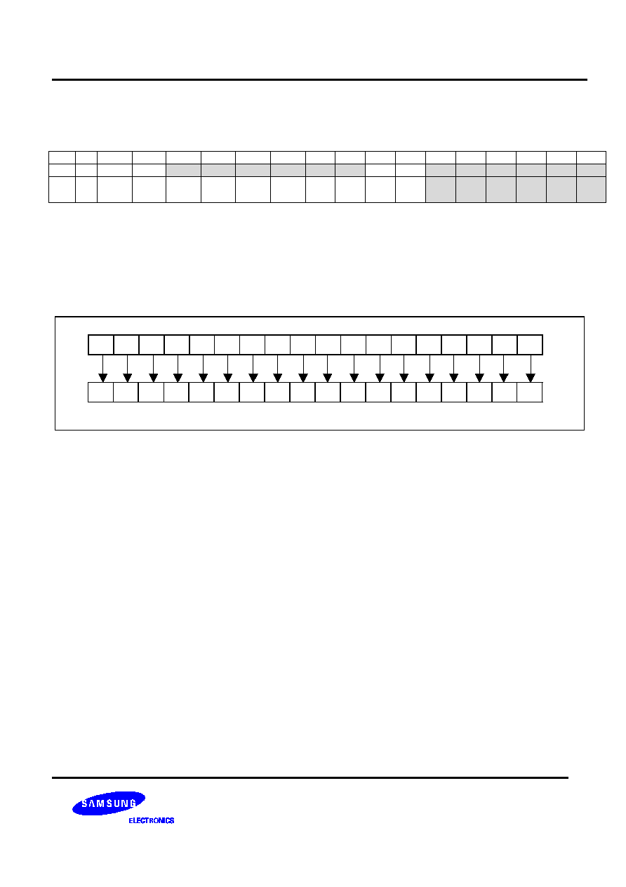
S6D0114 132-RGB X 176-DOT 1-CHIP DRIVER IC FOR 262,144-COLOR TFT-LCD DISPLAY
Preliminary
61
RAM Write Data Mask 1 (R23h)
RAM Write Data Mask 2 (R24h)
R/W
RS
DB15
DB14
DB13
DB12
DB11
DB10
DB9
DB8
DB7
DB6
DB5
DB4
DB3
DB2
DB1
DB0
W
1
0
0
WM11
WM10
WM9
WM8
WM7
WM6
0
0
WM5
WM4
WM3
WM2
WM1
WM0
W
1
0
0
0
0
0
0
0
0
0
0
WM
17
WM
16
WM
15
WM
14
WM
13
WM
12
WM17�0: In writing to the GRAM, these bits mask writing in a bit unit. When WM17 = 1, this bit masks the write data
of DB15 and does not write to the GRAM. Similarly, the WM14 to 0 bits mask the write data of DB14 to 0 in a bit unit.
For details, see the Graphics Operation Function section.
Please make sure the write data to GRAM (18-bit) is masked.
When 8-/16- bit interface is in use, the LSB of <R><B> write data will not be read.
When RGB interface is in use, this function is not available.
WM
17
WM
16
WM
15
WM
14
WM
13
WM
12
WM
11
WM
10
WM
9
WM
8
WM
7
WM
6
WM
5
WM
4
WM
3
WM
2
WM
1
WM
0
R5
R4
R3
R2
R1
R0
G5
G4
G3
G2
G1
G0
B5
B4
B3
B2
B1
B0
1-pixel
WM
17
WM
16
WM
15
WM
14
WM
13
WM
12
WM
11
WM
10
WM
9
WM
8
WM
7
WM
6
WM
5
WM
4
WM
3
WM
2
WM
1
WM
0
R5
R4
R3
R2
R1
R0
G5
G4
G3
G2
G1
G0
B5
B4
B3
B2
B1
B0
1-pixel
Figure 24. Write Mask and RAM Write Data

132-RGB X 176-DOT 1-CHIP DRIVER IC FOR 262,144-COLOR TFT-LCD DISPLAY
S6D0114
Preliminary
62
Gamma Control (R30h to R37h)
R/W
RS
DB15
DB14
DB13
DB12
DB11
DB10
DB9
DB8
DB7
DB6
DB5
DB4
DB3
DB2
DB1
DB0
W
1
0
0
0
0
0
PKP
12
PKP
11
PKP
10
0
0
0
0
0
PKP
02
PKP
01
PKP
00
W
1
0
0
0
0
0
PKP
32
PKP
31
PKP
30
0
0
0
0
0
PKP
22
PKP
21
PKP
20
W
1
0
0
0
0
0
PKP
52
PKP
51
PKP
50
0
0
0
0
0
PKP
42
PKP
41
PKP
40
W
1
0
0
0
0
0
PRP
12
PRP
11
PRP
10
0
0
0
0
0
PRP
02
PRP
01
PRP
00
W
1
0
0
0
0
0
PKN
12
PKN
11
PKN
10
0
0
0
0
0
PKN
02
PKN
01
PKN
00
W
1
0
0
0
0
0
PKN
32
PKN
31
PKN
30
0
0
0
0
0
PKN
22
PKN
21
PKN
20
W
1
0
0
0
0
0
PKN
52
PKN
51
PKN
50
0
0
0
0
0
PKN
42
PKN
41
PKN
40
W
1
0
0
0
0
0
PRN
12
PRN
11
PRN
10
0
0
0
0
0
PRN
02
PRN
01
PRN
00
PKP52�00: The gamma fine adjustment register for the positive polarity output
PRP12-00: The gradient adjustment register for the positive polarity output
PKN52-00: The gamma fine adjustment register for the negative polarity output
PRN12-00: The gradient adjustment register for the negative polarity output
For details, see the Gamma Adjustment Function.
S6D0114 132-RGB X 176-DOT 1-CHIP DRIVER IC FOR 262,144-COLOR TFT-LCD DISPLAY
Preliminary
63
Gate Scan Position (R40h)
R/W
RS
DB15
DB14
DB13
DB12
DB11
DB10
DB9
DB8
DB7
DB6
DB5
DB4
DB3
DB2
DB1
DB0
W
1
0
0
0
0
0
0
0
0
0
0
0
SCN4
SCN3
SCN2
SCN1
SCN0
SCN 4-0: Set the scanning starting position of the gate driver.
Scanning start position
SCN4
SCN3
SCN2
SCN1
SCN0
GS=0
GS=1
0
0
0
0
0
G1
G176
0
0
0
0
1
G9
G168
0
0
0
1
0
G17
G160
:
:
:
:
:
:
:
:
:
:
:
:
:
:
1
0
0
1
1
G153
G24
1
0
1
0
0
G161
G16
1
0
1
0
1
G169
G8
G1
G160
G161
G176
G1
G160
G161
G176
G16
G17
GS = 0
NL = 10010
SCN4-0 = 00000
GS = 1
NL = 10010
SCN4-0 = 00010
Note: Set NL4-0 on the gate scan end that does not exceed value 176
Figure 25. Relationship between NL and SCN set up value
132-RGB X 176-DOT 1-CHIP DRIVER IC FOR 262,144-COLOR TFT-LCD DISPLAY
S6D0114
Preliminary
64
Vertical Scroll Control (R41h)
R/W
RS
DB15
DB14
DB13
DB12
DB11
DB10
DB9
DB8
DB7
DB6
DB5
DB4
DB3
DB2
DB1
DB0
W
1
0
0
0
0
0
0
0
0
VL7
VL6
VL5
VL4
VL3
VL2
VL1
VL0
VL7-0: Specify scroll length at the scroll display for vertical smooth scrolling. Any raster-row from the first to 176
th
can be scrolled for the number of the raster-row. After 176
th
raster-row is displayed, the display restarts from the first
raster-row. The display-start raster-row (VL7-0) is valid when VLE1 = 1 or VLE2 = 1. The raster-row display is fixed
when VLE2-1 = 00.
VL7
VL6
VL5
VL4
VL3
VL2
VL1
VL0
Scroll length
0
0
0
0
0
0
0
0
0 raster-row
0
0
0
0
0
0
0
1
1 raster-row
0
0
0
0
0
0
1
0
2 raster-row
.
.
.
.
.
.
.
.
1
0
1
0
1
1
1
0
174 raster-row
1
0
1
0
1
1
1
1
175 raster-row
Note: Don't set any higher raster-row than 175 ("AF"H)
1
st
Screen Driving Position (R42h)
2
nd
Screen Driving Position (R43h)
R/W
RS
DB15
DB14
DB13
DB12
DB11
DB10
DB9
DB8
DB7
DB6
DB5
DB4
DB3
DB2
DB1
DB0
W
1
SE17
SE16
SE15
SE14
SE13
SE12
SE11
SE10
SS17
SS16
SS15
SS14
SS13
SS12
SS11
SS10
W
1
SE27
SE26
SE25
SE24
SE23
SE22
SE21
SE20
SS27
SS26
SS25
SS24
SS23
SS22
SS21
SS20
SS17�10: Specify the driving start position for the first screen in a line unit. The LCD driving starts from the `set value
+1' gate driver.
SE17�10: Specify the driving end position for the first screen in a line unit. The LCD driving is performed to the 'set
value + 1' gate driver. For instance, when SS17�10 = 07h and SE17�10 = 10h are set, the LCD driving is performed
from G8 to G17, and non-display driving is performed for G1 to G7, G18, and others. Ensure that SS17�10
SE17�10
AFh. For details, see the Screen-division Driving Function section.
SS27�10: Specify the driving start position for the second screen in a line unit. The LCD driving starts from the 'set
value + 1' gate driver. The second screen is driven when SPT = 1.
SE27�20: Specify the driving end position for the second screen in a line unit. The LCD driving is performed to the
'set value + 1' gate driver. For instance, when SPT = 1, SS27�20 = 20h, and SE27�20 = AFh are set, the LCD
driving is performed from G33 to G80. Ensure that SS17�10
SE17�10
SS27�20
SE27�20
AFh. For details,
see the Screen-division Driving Function section.

S6D0114 132-RGB X 176-DOT 1-CHIP DRIVER IC FOR 262,144-COLOR TFT-LCD DISPLAY
Preliminary
65
Horizontal RAM Address Position (R16h)
Vertical RAM Address Position (R17h)
R/W
RS
DB15
DB14
DB13
DB12
DB11
DB10
DB9
DB8
DB7
DB6
DB5
DB4
DB3
DB2
DB1
DB0
W
1
HEA
7
HEA
6
HEA
5
HEA
4
HEA
3
HEA
2
HEA
1
HEA
0
HSA
7
HSA
6
HSA
5
HSA
4
HSA
3
HSA
2
HSA
1
HSA
0
W
1
VEA
7
VEA
6
VEA
5
VEA
4
VEA
3
VEA
2
VEA
1
VEA
0
VSA
7
VSA
6
VSA
5
VSA
4
VSA
3
VSA
2
VSA
1
VSA
0
HSA7-0/HEA7-0: Specify the horizontal start/end positions of a window for access in memory. Data can be written
to the GRAM from the address specified by HEA 7-0 from the address specified by HSA7-0. Note that an address
must be set before RAM is written. Ensure 00h
HSA7-0
HEA7-0
83h.
VSA7-0/VEA7-0: Specify the vertical start/end positions of a window for access in memory. Data can be written to
the GRAM from the address specified by VEA7-0 from the address specified by VSA7-0. Note that an address must
be set before RAM is written. Ensure 00h
VSA7-0
VEA7-0
AFh.
Window address
0000H
AF83H
HSA
HEA
VSA
VEA
GRAM address space
Window address setting range
"00"h
HSA7-0
HEA7-0
"83"h
"00"h
VSA7-0
VEA7-0
"AF"h
NOTE: 1. Ensure that the window address area is within the GRAM address space
2. In high-speed write mode, data are written to GRAM in four-words.
Thus, dummy write operations should be inserted depending on the window address
area. For details, see the High-Speed Burst RAM Write Function section
Figure 26. Window address setting range

132-RGB X 176-DOT 1-CHIP DRIVER IC FOR 262,144-COLOR TFT-LCD DISPLAY
S6D0114
Preliminary
66
RESET FUNCTION
The S6D0114 is internally initialized by RESET input. The reset input must be held for at least 1 ms. Do not access
the GRAM or initially set the instructions until the R-C oscillation frequency is stable after power has been supplied
(10 ms).
Instruction Set Initialization
1. Start oscillation executed
2. Driver output control (NL4�0 = 10101, SS = 0, CS = 0, EPL=0)
3. LCD driving AC control (FLD1-0 = 01, B/C = 0, EOR = 0, NW5�0 = 00000)
4. Power control 1 (SAP2-0 = 000, BT2-0 = 000, DC2�0 = 000, AP2�0 = 000: LCD power off, SLP = 0, STB = 0:
Standby mode off)
5. Power control 2 (CAD = 0, VRN4-0 = 00000, VRP4-0 = 00000)
6. Entry mode set (HWM = 0, I/D1-0 = 11: Increment by 1, AM = 0: Horizontal move, LG2�0 = 000: Replace mode,
BGR=0)
7. Compare register (CP17�0: 00/0000/0000/0000/0000)
8. Display control 1 (PT1-0 = 00, VLE2�1 = 00: No vertical scroll, SPT = 0, GON = 0, DTE = 0, CL = 0: 260K-color
mode, REV = 0, D1�0 = 00: Display off)
9. Display control 2 (FP3-0=0101, BP3-0=0011, BLP13-0=0010, BLP23-0=0010
)
10. Frame cycle control (NO1-0 = 00, SDT1-0 = 00, EQ1-0 = 00: no equalization, DIV1-0 = 00: 1-divided clock,
RTN3-0 = 0000: 16 clock cycle in 1H period)
11. External display interface (RIM1-0=00:18-bit RGB interface, DM1-0=00: operated by internal clock, RM=0:
system interface)
12. Power control 3 (VC2-0 = 000)
13. Power control 4 (VRL3-0 = 0000, PON=0, VRH3-0 = 0000)
14. Power control 5 (VCOMG = 0, VDV4-0 = 00000, VCM4-0 = 00000)
15. RAM address set (AD15�0 = 0000h)
16. RAM write data mask (WM15�0 = 0000h: No mask)
17. Gamma control
(PKP02�00 = 000, PKP12�10 = 000, PKP22�20 = 000, PKP32�30 = 000,
PK42�40 = 000, PKP52�50 = 000, PRP02�00 = 000, PRP12�10 = 000)
(PKN02�00 = 000, PKN12�10 = 000, PKN22�20 = 000, PKN32�30 = 000,
PKN42�40 = 000, PKN52�50 = 000, PRN02�00 = 000, PRN12�10 = 000)
18. Gate scanning starting position (SCN4-0 = 00000)
19. Vertical scroll (VL7�0 = 0000000)
20. 1st screen division (SE17-10 = 11111111, SS17-10 = 00000000)
21. 2nd screen division (SE27-20 = 11111111, SS27-20 = 00000000)
22. Horizontal RAM address position (HEA7-0 = 10000011, HSA7-0 = 00000000)
23. Vertical RAM address position (VEA7-0 = 10101111, VSA7-0 = 00000000)
GRAM Data Initialization
GRAM is not automatically initialized by reset input but must be initialized by software while display is off (D1-0 =
00).
Output Pin Initialization
1. LCD driver output pins (Source output) : Output VSS level
(Gate output) : Output Vgoff level
2. Oscillator output pin (OSC2): Outputs oscillation sign
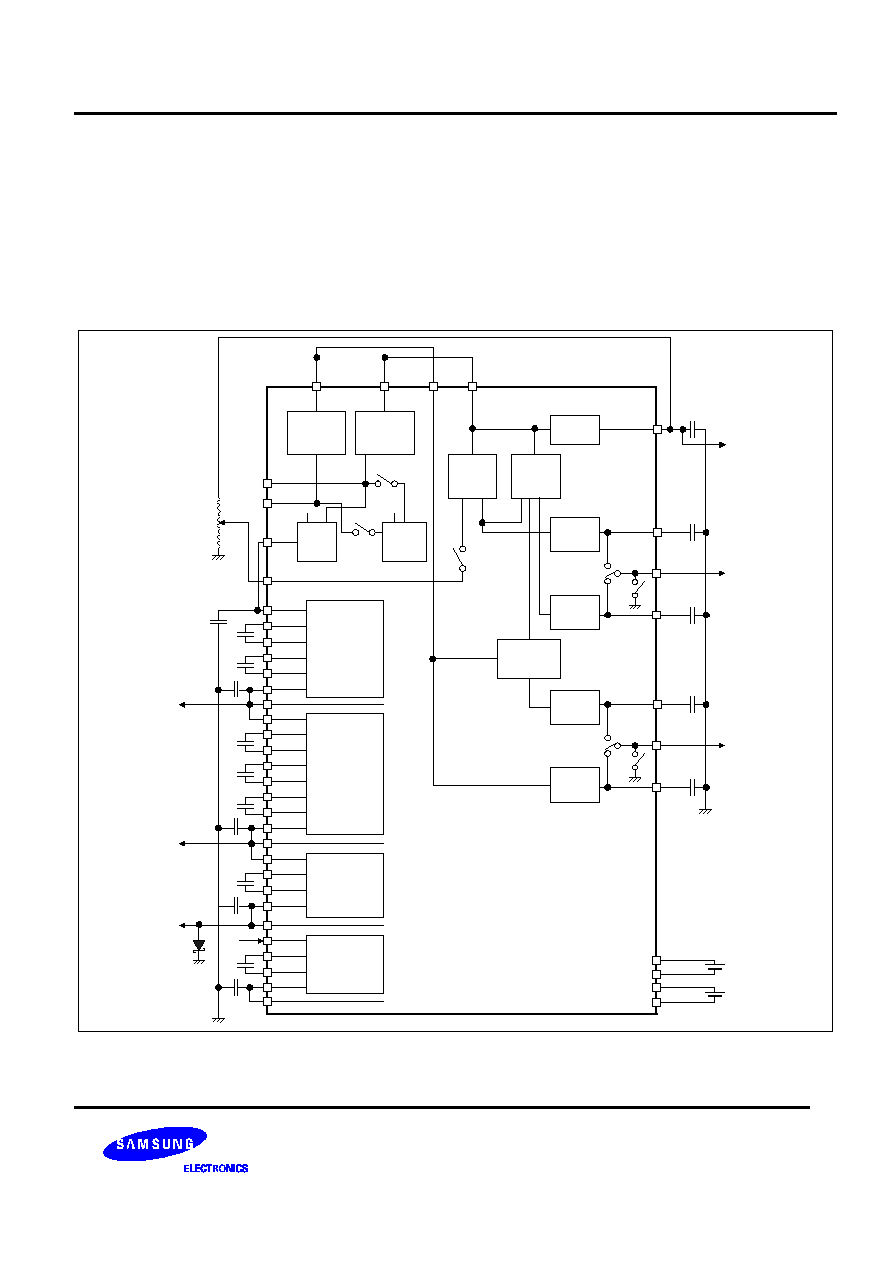
S6D0114 132-RGB X 176-DOT 1-CHIP DRIVER IC FOR 262,144-COLOR TFT-LCD DISPLAY
Preliminary
67
POWER SUPPLY CIRCUIT
The following figure shows a configuration of the voltage generation circuit for S6D0114. The step-up circuits consist
of step-up circuits 1 to 4. Step-up circuit1 doubles or triples the voltage supplied to Vci1, and that voltage is doubled,
tripled, or quadrupled in step-up circuit2. Step-up circuit3 reverses the VGH level with reference to VSS or VBS and
generates the VGL level. Step-up circuit 4 reverses the Vci level with reference to VSS and generates the VCL level.
These step-up circuits generate power supplies AVDD, GVDD, VGH, VGL, Vgoff, and Vcom. Reference voltages
GVDD, Vcom, and Vgoff for the grayscale voltage are amplified in amplification circuits 1 and 2 from the internal-
voltage adjustment circuit or the REGP or REGN voltage, and generate each level depending on that voltage.
Connect Vcom to the TFT panel.
Amplfiication
circuit2
(Vgoff
adjustment)
Amplification
circuit1
(GVDD
adjustment)
VcomH
adjustment
circuit
Vcom
amplitude
adjustment
circuit
GVDD
Voltage
adjustment
circuit
Regulator
Vciout
Vci
Vci
VcomR
GVDD output
amplifier
GVDD
Step-up
circuit 1
Step-up
circuit 2
Step-up
circuit 3
VREG2
OUT
VREG1
OUT
VREG2
VREG1
REGP
REGN
Adjust VcomH
voltage (when
using an external
variable resistor)
Vci
When
using
Vciout
Vci1
C11-
C11+
C12-
C12+
VLOUT1
DDVDH
Vci2
C21-
C21+
C22-
C22+
C23-
C23+
VLOUT2
VGH
Vci3
C31-
C31+
VLOUT3
VGL
Vci4
C41-
C41+
VLOUT4
VCL
VGL
VGH
AVDD
VcomH
output
amplifier
VcomL
output
amplifier
VcomH
Vcom
VcomL
VgoffH
output
amplifier
VgoffL
output
amplifier
VgoffH
Vgoffout
VgoffL
VgoffH
amplitude
adjustment
circuit
Vss
Vss
Vdd
Vci
Step-up
circuit 4
Figure 27. Configuration of the Internal Power-Supply Circuit
Notes:
Use the 1uF capacitor.
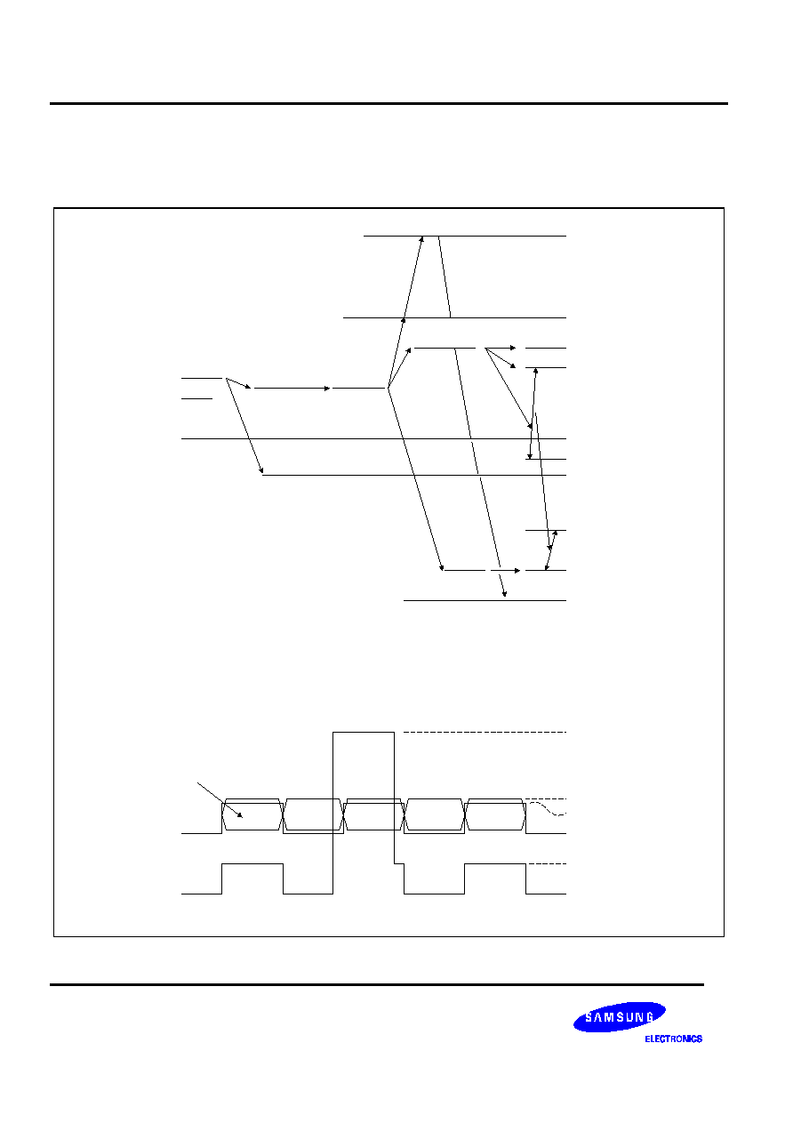
132-RGB X 176-DOT 1-CHIP DRIVER IC FOR 262,144-COLOR TFT-LCD DISPLAY
S6D0114
Preliminary
68
PATTERN DIAGRAMS FOR VOLTAGE SETTING
The following figure shows a pattern diagram for the voltage setting and an example of waveforms.
VGH(+7 ~ +20V)
AVDD(+3.5 ~ +5.5V)
DDVDH
VREG1OUT
GVDD(+3.0 ~ +5.0V)
VDH
VcomH(+3.0 ~ VDH)
VCOM4-0
VDV4-0
BT2-0
VRH3-0
Vci1
(-1 times)
BT2-0
VRL3-0
(-1 times)
VcomL(VCL+0.5 to 1.0V)
VCL
VgoffH(to -5.0V)
VgoffL
(VGL+0.5 to -16.0V)
VGL(-9 to -16.5V)
VREG2OUT
Vci(2.5V ~ 3.3V)
VDD(1.8V ~ 3.3V)
VSS(0V)
VC2-0
Note:
Adjust the conditions of AVDD-GVDD>0.5V, VcomL-VCL>0.5V, and Vgoff-VGL>0.5V with loads because they
differ depending on the display load to be driven. In addition, Vci can be directly input to Vci1.
VGH
GVDD(VDH)
VcomH
VcomL
VgoffH
VgoffL
VCOM
Sn(source output)
Gn(Gate output)
Figure 28. Pattern diagram and an example of waveforms
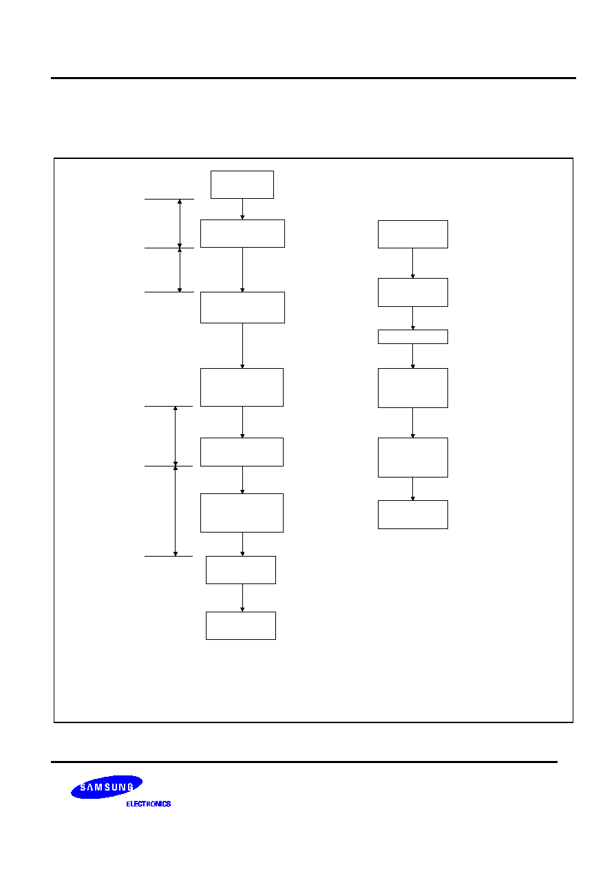
S6D0114 132-RGB X 176-DOT 1-CHIP DRIVER IC FOR 262,144-COLOR TFT-LCD DISPLAY
Preliminary
69
SET UP FLOW OF POWER SUPPLY
Apply the power in a sequence as shown in the following figure. The stable time of the oscillation circuit, step-up
circuit, and operational amplifier depend on the external resistor or capacitance.
10ms or more
(Stable time of the
oscillation circuit)
Power Supply
(Vdd on)
Power-on reset
and display off
1ms
Issues instructions for
power supply setting (1)
Bits for display off.
DTE=0
D1-0=00
GON=0
PON=0
Normal Display
Bits for display
on: DTE =1, D1-
0=11, GON=1
Bits for power-supply
initial
setting: VCOM, VC2-
0, VRH3-
0, CAD, VRL3-
0, VCM4-0, VDV4-
0, VRN4-0, VRP4-0
(setting of the source-
driver grayscale
voltage)
Issues instruction for
power supply setting (2)
Bits for power-supply
operation start
setting: BT2-0, DC2-
0, AP2-0
Bits for source-driver
operational amplifier
operaton-start
setting: SAP2-0
Bits for step-up
circuit3 operation
start PON=1
Issues instruction for
power supply setting (3)
Display off
Bits for display
off: DTE =0, D1-
0=00, GON=0
Instruction for
power supply setting(1)
Bits for source-driver
operational amplifier
operation-stop setting:
SAP2-0
Instruction for
power supply setting(2)
Bits for power supply
stop setting: AP2-0
for operational
amplifier, DC2-0 for
step-up circuit
Display off
sequence*
Power supply
(Vdd off)
Issues instruction for
other mode setting
Display-on
Sequence*
Diplay on
Bits for display
on: DTE =1, D1-
0=11, GON=1
50ms or more
(Stable times of step-up
circuit 1 and 2)
200ms or more
(Stable time of the step-
up operational
amplifier)
Power-on sequence
Power-off sequence
Figure 29. Set up Flow of Power Supply
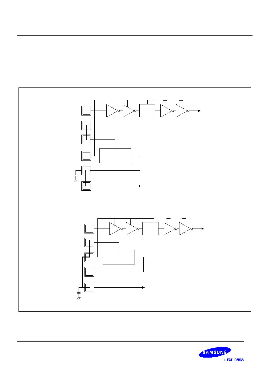
132-RGB X 176-DOT 1-CHIP DRIVER IC FOR 262,144-COLOR TFT-LCD DISPLAY
S6D0114
Preliminary
70
VOLTAGE REGULATION FUNCTION
The S6D0114 have internal voltage regulator. Voltage regulation function is controlled by PregB pin.
If PregB= "H", voltage regulation is stopped. PregB= "L" enables internal voltage regulation function.
By use of this function, internal logic circuit damage can be prohibited. Furthermore, power consumption also be
obtained. Detailed function description and application setup is described in the following diagram.
VOLTAGE
REGULATOR
Internal VDD
(1.9V)
VDD3
(External Power)
Range: 2.5~3.3V
RVDD
PREGB
PregB= 'L' : REGULATOR ON
VDD
INPUT
Level
Shifter
Internal VDD
INTERNAL
LOGIC
GND
(a) Voltage regulation function enabled
VOLTAGE
REGULATOR
Internal VDD
INPUT
PREGB
Level
Shifter
Internal VDD
INTERNAL
LOGIC
VDD
(External Power)
1.8~2.5V
VDD3
RVDD
PregB= 'H' : REGULATOR OFF
(b) Voltage regulation function disabled
Figure 30. Voltage regulation function

S6D0114 132-RGB X 176-DOT 1-CHIP DRIVER IC FOR 262,144-COLOR TFT-LCD DISPLAY
Preliminary
71
INTERFACE SPECIFICATION
The S6D0114 incorporates a system interface, which is used to set instructions, and an external display interface,
which is used to display motion pictures. Selecting these interfaces to match the screen data (motion picture or still
picture) enables efficient transfer of data for display.
The external display interface includes RGB interface and VSYNC interface. This allows flicker-free screen update.
When RGB interface is selected, the synchronization signals (VSYNC, HSYNC, and DOTCLK) are available for use
in operating the display. The data for display (PD17-0) is written according to the values of the data enable signal
(ENABLE) and data valid signal (VLD), in synchronization with the VSYNC, HSYNC, and DOTCLK signals. In
addition, using the window address function enables rewriting only to the internal RAM area to display motion
pictures. Using this function also enables simultaneously display of the motion picture area and the RAM data that
was written.
While displaying motion pictures, the data for display should be written in high-speed write mode, which achieves
both low power consumption and high-speed access via RGB interface or VSYNC interface.
The internal display operation is synchronized with the frame synchronization signal (VSYNC) in VSYNC interface
mode. When writing to the internal RAM is done within the required time after the falling edge of VSYNC, motion
pictures can be displayed via the conventional interface. There are some limitations on the timing and methods of
writing to RAM. See the section on the external display interface.
The S6D0114 has four operation modes for each display state. These settings are specified by control instructions
for external display interface. Transitions between modes should follow the transition flow.
Table 24. Display Operation Mode and RAM Access Selection
Operation Mode
RAM Access Selection
(RM)
Display Operation Mode
(DM1-0)
Internal Clock Operation
(Displaying still picture)
System interface
(RM=0)
Internal clock operation
(DM1-0=00)
RGB interface (1)
(Displaying motion picture)
RGB interface
(RM=1)
RGB interface
(DM1-0=01)
RGB interface (2)
(Rewriting still picture while
displaying motion pictures)
System interface
(RM=0)
RGB interface
(DM1-0=01)
VSYNC interface
(Displaying motion Pictures)
System interface
(RM=0)
VSYNC interface
(DM1-0=10)
NOTES:
1) Instruction registers can only be set via system interface.
2) RGB interface and VSYNC interface cannot be used at the same time.
3) RGB interface mode cannot be set during operations.
4) For mode transitions, see the section on the external display interface.
5) RGB interface VSYNC interface modes should be used in high-speed write mode (HWM = 1).
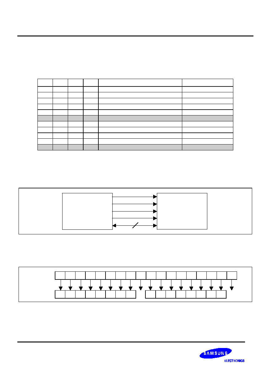
132-RGB X 176-DOT 1-CHIP DRIVER IC FOR 262,144-COLOR TFT-LCD DISPLAY
S6D0114
Preliminary
72
SYSTEM INTERFACE
S6D0114 is enabling to set instruction and access to RAM by selecting IM3/2/1/0 pin in the system interface mode.
Table 25. IM Bits and System Interface
IM3
IM2
IM1
IM0
System Interface
DB Pin
0
0
0
0
68-system 16-bit interface
DB17 to10, 8 to1
0
0
0
1
68-system 8-bit interface
DB17 to10
0
0
1
0
80-system 16-bit interface
DB17 to10, 8 to1
0
0
1
1
80-system 8-bit interface
DB17 to10
0
1
0
*
Serial peripheral interface (SPI)
DB1 to 0
0
1
1
*
Setting disabled
-
1
0
0
0
68-system 18-bit interface
DB17 to 0
1
0
0
1
68-system 9-bit interface
DB17 to 9
1
0
1
0
80-system 18-bit interface
DB17 to 0
1
0
1
1
80-system 9-bit interface
DB17 to 9
1
1
*
*
Setting disabled
-
68/80-SYSTEM 18-BIT BUS INTERFACE
Setting the IM3/2/1/0 (interface mode) to the VDD3/VSS/VSS/vSS level allows 68-system 18-bit parallel data
transfer. Setting the IM3/2/1/0 to the VDD3/GND/VDD3/GND level allows 80-system 18-bit parallel data transfer.
MPU
CSn
A1
/WR
/RD
D17-D0
S6D0114
CSB
RS
/WR
/RD
DB17-DB0
18
Figure 31. Interface with the 18-bit Microcomputer
68/80-SYSTEM 18-bit interface data FORMAT
DB
17
DB
16
DB
15
DB
14
DB
13
DB
12
DB
11
DB
10
DB
9
DB
8
DB
7
DB
6
DB
5
DB
4
DB
3
DB
2
DB
1
DB
0
Input
IB
15
IB
14
IB
13
IB
12
IB
11
IB
10
IB
9
IB
8
IB
7
IB
6
IB
5
IB
4
IB
3
IB
2
IB
1
IB
0
Instruction
Figure 32. Instruction format for 18-bit Interface
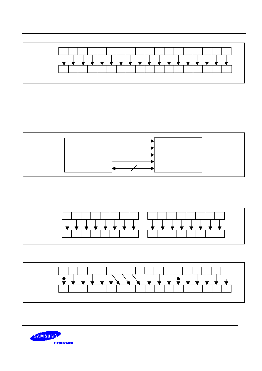
S6D0114 132-RGB X 176-DOT 1-CHIP DRIVER IC FOR 262,144-COLOR TFT-LCD DISPLAY
Preliminary
73
DB
17
DB
16
DB
15
DB
14
DB
13
DB
12
DB
11
DB
10
DB
9
DB
8
DB
7
DB
6
DB
5
DB
4
DB
3
DB
2
DB
1
DB
0
Input
R5
R4
R3
R2
R1
R0
G5
G4
G3
G2
G1
G0
B5
B4
B3
B2
B1
B0
GRAM data
1-pixel
*262,144 -color display is available in 18-bit system interface.
Figure 33. RAM Data Write format for 18-bit Interface
68/80-SYSTEM 16-BIT BUS INTERFACE
Setting the IM3/2/1/0 (interface mode) to the VSS/VSS/VSS/VSS level allows 68-system 16-bit parallel data transfer.
Setting the IM3/2/1/0 to the VSS/VSS/VDD3/VSS level allows 80-system 16-bit parallel data transfer.
MPU
CSn*
A1
HWR*
(RD*)
D15-D0
S6D0114
CSB
/WR
/RD
DB17-10, DB8-1
16
Figure 34. Interface with the 16-bit Microcomputer
68/80-SYSTEM 16-bit interface data FORMAT
Input
DB
17
DB
16
DB
15
DB
14
DB
13
DB
12
DB
11
DB
10
DB
8
DB
7
DB
6
DB
5
DB
4
DB
3
DB
2
DB
1
IB
15
IB
14
IB
13
IB
12
IB
11
IB
10
IB
9
IB
8
IB
7
IB
6
IB
5
IB
4
IB
3
IB
2
IB
1
IB
0
Instruction
Instruction code
Input
DB
17
DB
16
DB
15
DB
14
DB
13
DB
12
DB
11
DB
10
DB
8
DB
7
DB
6
DB
5
DB
4
DB
3
DB
2
DB
1
IB
15
IB
14
IB
13
IB
12
IB
11
IB
10
IB
9
IB
8
IB
7
IB
6
IB
5
IB
4
IB
3
IB
2
IB
1
IB
0
Instruction
Instruction code
Figure 35. Instruction format for 16-bit Interface
Input
DB
17
DB
16
DB
15
DB
14
DB
13
DB
12
DB
11
DB
10
DB
8
DB
7
DB
6
DB
5
DB
4
DB
3
DB
2
DB
1
R5
R4
R3
R2
R1
R0
G5
G4
G3
G2
G1
G0
B5
B4
B3
B2
B1
B0
GRAM data
1-pixel
*65,536-color display is available in the 16-bit system interface.
Figure 36. RAM Data Write format for 16-bit Interface
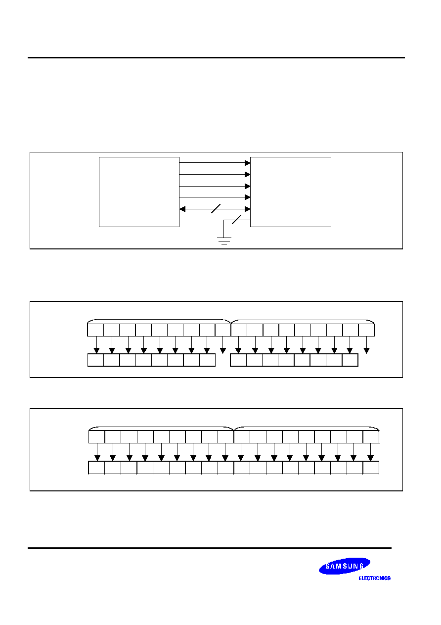
132-RGB X 176-DOT 1-CHIP DRIVER IC FOR 262,144-COLOR TFT-LCD DISPLAY
S6D0114
Preliminary
74
68/80-SYSTEM 9-BIT BUS INTERFACE
Setting the IM3/2/1/0 (interface mode) to the VDD3/VSS/VSS/VDD3 level allows 68-system 9-bit parallel data
transfer using pins DB17�DB9. Setting the IM3/2/1/0 to be VDD3/VSS/VDD3/VDD3 level allows 80-system 9-bit
parallel data transfer. The 16-bit instructions and RAM data are divided into nine upper/lower bits and the transfer
starts from the upper nine bits. Fix unused pins DB8�DB0 to the VDD 3 or VSS level. Note that the upper bytes must
also be written when the index register is written.
MPU
CSn*
A1
HWR*
(RD*)
D15-D0
S6D0101
CS*
RS
WR*
(RD*)
DB17-DB9
9
DB8-DB0
9
MPU
CSn*
A1
HWR*
(RD*)
D15-D0
S6D0101
CS*
RS
WR*
(RD*)
DB17-DB9
9
DB8-DB0
9
Figure 37. Interface to 9-bit Microcomputer
68/80-SYSTEM 9-bit interface data FORMAT
Input
IB
15
IB
14
IB
13
IB
12
IB
11
IB
10
IB
9
IB
8
IB
7
IB
6
IB
5
IB
4
IB
3
IB
2
IB
1
IB
0
Instruction
Instruction code
1st transfer(upper)
2nd transfer(lower)
DB
17
DB
16
DB
15
DB
14
DB
13
DB
12
DB
11
DB
10
DB
9
DB
17
DB
16
DB
15
DB
14
DB
13
DB
12
DB
11
DB
10
DB
9
Input
IB
15
IB
14
IB
13
IB
12
IB
11
IB
10
IB
9
IB
8
IB
7
IB
6
IB
5
IB
4
IB
3
IB
2
IB
1
IB
0
Instruction
Instruction code
1st transfer(upper)
2nd transfer(lower)
DB
17
DB
16
DB
15
DB
14
DB
13
DB
12
DB
11
DB
10
DB
9
DB
17
DB
16
DB
15
DB
14
DB
13
DB
12
DB
11
DB
10
DB
9
Figure 38. Instruction format for 9-bit Interface
Input
R5
R4
R3
R2
R1
R0
G5
G4
G3
G2
G1
G0
B5
B4
B3
B2
B1
B0
GRAM data
1-pixel
*262,144-color display is available in the 9-bit system interface
1st transfer(upper)
2nd transfer(lower)
DB
17
DB
16
DB
15
DB
14
DB
13
DB
12
DB
11
DB
10
DB
9
DB
17
DB
16
DB
15
DB
14
DB
13
DB
12
DB
11
DB
10
DB
9
Figure 39. RAM Data Write format for 9-bit Interface

S6D0114 132-RGB X 176-DOT 1-CHIP DRIVER IC FOR 262,144-COLOR TFT-LCD DISPLAY
Preliminary
75
NOTE: Transfer synchronization function for a 9-bit bus interface
The S6D0114 supports the transfer synchronization function, which resets the upper/lower counter to count
upper/lower 9-bit data transfer in the 9-bit bus interface. Noise causing transfer mismatch between the nine upper
and lower bits can be corrected by a reset triggered by consecutively writing a "00"H instruction four times. The next
transfer starts from the upper nine bits. Executing synchronization function periodically can recover any runaway in
the display system.
"00"H
"00"H
"00"H
"00"H
Upper or
Lower
Upper
Lower
RS
RD
WR
DB17
~DB9
(1)
(2)
(3)
(4)
9-bit transfer sync.
"00"H
"00"H
"00"H
"00"H
Upper or
Lower
Upper
Lower
RS
RD
WR
DB17
~DB9
(1)
(2)
(3)
(4)
9-bit transfer sync.
Figure 40. 9-bit Transfer Synchronization
68/80-SYSTEM 8-BIT BUS INTERFACE
Setting the IM3/2/1/0 (interface mode) to the VSS/vSS/VSS/VDD3 level allows 68-system 8-bit parallel data transfer.
Setting the IM3/2/1/0 to the VSS/VSS/VDD3/VDD3 level allows 80-system 8-bit parallel data transfer. The 16-bit
instructions and RAM data are divided into eight upper/lower bits and the transfer starts from the upper eight bits. Fix
unused pins DB9�DB0 to the VDD3 or VSS level. Note that the upper bytes must also be written when the index
register is written.
MPU
CSn
A1
/WR
/RD
D7-D0
S6D0114
CSB
RS
/WR
/RD
DB15-DB8
8
DB7-DB0
8
Figure 41. Interface with the 8-bit Microcomputer
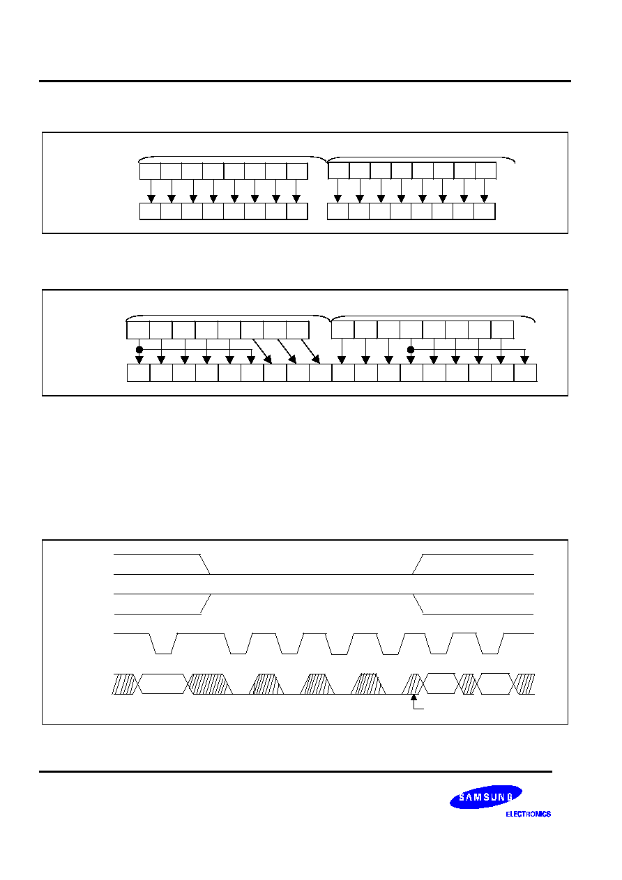
132-RGB X 176-DOT 1-CHIP DRIVER IC FOR 262,144-COLOR TFT-LCD DISPLAY
S6D0114
Preliminary
76
68/80-SYSTEM 8-bit interface data FORMAT
Input
DB
17
DB
16
DB
15
DB
14
DB
13
DB
12
DB
11
DB
10
IB
15
IB
14
IB
13
IB
12
IB
11
IB
10
IB
9
IB
8
IB
7
IB
6
IB
5
IB
4
IB
3
IB
2
IB
1
IB
0
Instruction
Instruction code
1st transfer(upper)
2nd transfer(lower)
DB
17
DB
16
DB
15
DB
14
DB
13
DB
12
DB
11
DB
10
Input
DB
17
DB
16
DB
15
DB
14
DB
13
DB
12
DB
11
DB
10
IB
15
IB
14
IB
13
IB
12
IB
11
IB
10
IB
9
IB
8
IB
7
IB
6
IB
5
IB
4
IB
3
IB
2
IB
1
IB
0
Instruction
Instruction code
1st transfer(upper)
2nd transfer(lower)
DB
17
DB
16
DB
15
DB
14
DB
13
DB
12
DB
11
DB
10
Figure 42. Instruction format for 8-bit Interface
Input
DB
17
DB
16
DB
15
DB
14
DB
13
DB
12
DB
11
DB
10
R5
R4
R3
R2
R1
R0
G5
G4
G3
G2
G1
G0
B5
B4
B3
B2
B1
B0
GRAM data
1-pixel
1st transfer(upper)
2nd transfer(lower)
DB
17
DB
16
DB
15
DB
14
DB
13
DB
12
DB
11
DB
10
Figure 43. RAM Data Write format for 8-bit Interface
NOTE: Transfer synchronization function for an 8-bit bus interface
The S6D0114 supports the transfer synchronization function, which resets the upper/lower counter to count
upper/lower 8-bit data transfer in the 8-bit bus interface. Noise causing transfer mismatch between the eight upper
and lower bits can be corrected by a reset triggered by consecutively writing a "00"H instruction four times. The next
transfer starts from the upper eight bits. Executing synchronization function periodically can recover any runaway in
the display system
"00"H
"00"H
"00"H
"00"H
Upper or
Lower
Upper
Lower
RS
RD
WR
DB17
~DB10
(1)
(2)
(3)
(4)
8-bit transfer sync.
"00"H
"00"H
"00"H
"00"H
Upper or
Lower
Upper
Lower
RS
RD
WR
DB17
~DB10
(1)
(2)
(3)
(4)
8-bit transfer sync.
Figure 44. 8-bit Transfer Synchronization
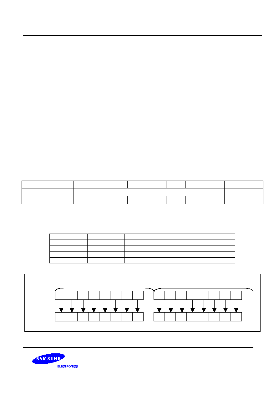
S6D0114 132-RGB X 176-DOT 1-CHIP DRIVER IC FOR 262,144-COLOR TFT-LCD DISPLAY
Preliminary
77
SERIAL DATA TRANSFER
Setting the IM3 pin to the VSS level allows serial peripheral interface (SPI) transfer, using the chip select line (CS*),
serial transfer clock line (SCL), serial input data (SDI), and serial output data (SDO). For a serial interface, the
IM0/ID pin function uses an ID pin. If the chip is set up for serial interface, the DB17-2 pins that are not used must be
fixed at VDD3 or VSS.
The S6D0114 initiates serial data transfer by transferring the start byte at the falling edge of CSB input. It ends serial
data transfer at the rising edge of CSB input.
The S6D0114 is selected when the 6-bit chip address in the start byte matches the 6-bit device identification code
that is assigned to the S6D0114. When selected, the S6D0114 receives the subsequent data string. The LSB of the
identification code can be determined by the ID pin. The five upper bits must be 01110. Two different chip addresses
must be assigned to a single S6D0114 because the seventh bit of the start byte is used as a register select bit (RS):
that is, when RS = 0, data can be written to the index register or status can be read, and when RS = 1, an instruction
can be issued or data can be written to or read from RAM. Read or write is selected according to the eighth bit of the
start byte (R/W bit). The data is received when the R/W bit is 0, and is transmitted when the R/W bit is 1.
After receiving the start byte, the S6D0114 receives or transmits the subsequent data byte-by-byte. The data is
transferred with the MSB first. All S6D0114 instructions are 16 bits. Two bytes are received with the MSB first (DB17
to 0), then the instructions are internally executed. After the start byte has been received, the first byte is fetched as
the upper eight bits of the instruction and the second byte is fetched as the lower eight bits of the instruction.
Four bytes of RAM read data after the start byte are invalid. The S6D0114 starts to read correct RAM data from the
fifth byte.
Table 26. Start Byte Format
Transfer bit
S
1
2
3
4
5
6
7
8
Device ID code
RS
R/W
Start byte format
Transfer start
0
1
1
1
0
ID
NOTE: ID bit is selected by the IM0/ID pin.
Table 27. RS and R/W Bit Function
RS
RW
Function
0
0
Set index register
0
1
Read status
1
0
Writes instruction or RAM data
1
1
Reads instruction or RAM data
IB
15
IB
14
IB
13
IB
12
IB
11
IB
10
IB
9
IB
8
IB
7
IB
6
IB
5
IB
4
IB
3
IB
2
IB
1
IB
0
Instruction
Instruction code
D15
D14
D13
D12
D11
D10
D9
D8
D7
D6
D5
D4
D3
D2
D1
D0
Input
1st transfer(upper)
2nd transfer(lower)
IB
15
IB
14
IB
13
IB
12
IB
11
IB
10
IB
9
IB
8
IB
7
IB
6
IB
5
IB
4
IB
3
IB
2
IB
1
IB
0
Instruction
Instruction code
D15
D14
D13
D12
D11
D10
D9
D8
D7
D6
D5
D4
D3
D2
D1
D0
Input
1st transfer(upper)
2nd transfer(lower)
Figure 45. Instruction format for Serial Data Transfer
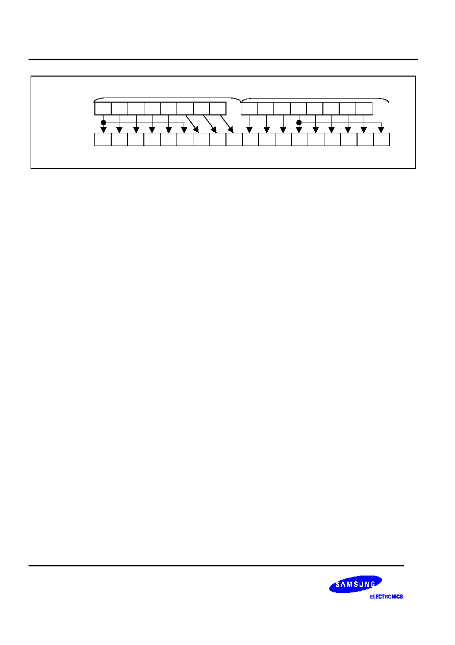
132-RGB X 176-DOT 1-CHIP DRIVER IC FOR 262,144-COLOR TFT-LCD DISPLAY
S6D0114
Preliminary
78
Input
R5
R4
R3
R2
R1
R0
G5
G4
G3
G2
G1
G0
B5
B4
B3
B2
B1
B0
GRAM data
1-pixel
*65,536-color display is possible using the serial interface.
1st transfer(upper)
2nd transfer(lower)
D15
D14
D13
D12
D11
D10
D9
D8
D7
D6
D5
D4
D3
D2
D1
D0
Input
R5
R4
R3
R2
R1
R0
G5
G4
G3
G2
G1
G0
B5
B4
B3
B2
B1
B0
GRAM data
1-pixel
*65,536-color display is possible using the serial interface.
1st transfer(upper)
2nd transfer(lower)
D15
D14
D13
D12
D11
D10
D9
D8
D7
D6
D5
D4
D3
D2
D1
D0
Figure 46. RAM Data Write format for Serial Data Transfer

S6D0114 132-RGB X 176-DOT 1-CHIP DRIVER IC FOR 262,144-COLOR TFT-LCD DISPLAY
Preliminary
79
1 2 3 4 5 6 7 8 9 10 11 12 13 14 15 16 17 18 19 20 21 22 23 24
0 1 1 1 0 ID R RW
DB DB DB DB DB DB DB DB DB DB DB DB DB DB DB DB
15 14 13 12 11 10 9 8 7 6 5 4 3 2 1 0
Device ID
RS R/W
Start byte
Index register setting instruction RAM data write
DB DB DB DB DB DB DB DB DB DB DB DB DB DB DB DB
15 14 13 12 11 10 9 8 7 6 5 4 3 2 1 0
Status read instruction read RAM data read
A) Timing Basic Data Transfer through Clock Synchronized Serial Bus Interface
Transfer start
Transfer end
B) Timing of Consecutive Data-Transfer through Clock-synchronized serial Bus Interface
Start byte
Instruction 1: upper
Instruction 2: lower
Instruction 2: upper
1 2 3 4 5 6 7 8 9 10 11 12 13 14 15 16 17 18 19 20 21 22 23 24 25 26 27 28 29 30 31 32
Instruction 1: execution time
End
Start
NOTE: The first byte after the start byte is always the upper eight bits.
SCL
(input)
SDI
(input)
SDO
(output)
SCL
(input)
SDI
(input)
CS*
(input)
CS*
(input)
C) RAM-Data Read-Transfer Timing
Start byte
RS=1
R/W=1
Dummy
read 1
Dummy
read 2
Dummy
read 3
Dummy
read 4
Dummy
read 5
RAM read:
upper 8-bits
RAM read:
lower 8-bits
Start
End
NOTE: 5-byte of RAM read data after the start byte are invalid.
The S6D0114 starts to read the correct RAM data from sixth byte
SCL
(input)
SDI
(input)
SDO
(output)
CS*
(input)
Figure 47. Procedure for transfer on clock synchronized serial bus interface

132-RGB X 176-DOT 1-CHIP DRIVER IC FOR 262,144-COLOR TFT-LCD DISPLAY
S6D0114
Preliminary
80
CS*
(input)
Start byte
RS=1
R/W=1
SDI
(input)
Dummy
read 1
Status read
upper 8-bit
Status read
lower 8-bit
Start
End
NOTE: 2-byte of the RAM read after the start byte is invalid.
The S6D0114 starts to read the correct RAM data from the third data.
D) Status Read/Instruction Read
SDO
(output)
Figure 48. Procedure for transfer on clock synchronized serial bus interface (continued)
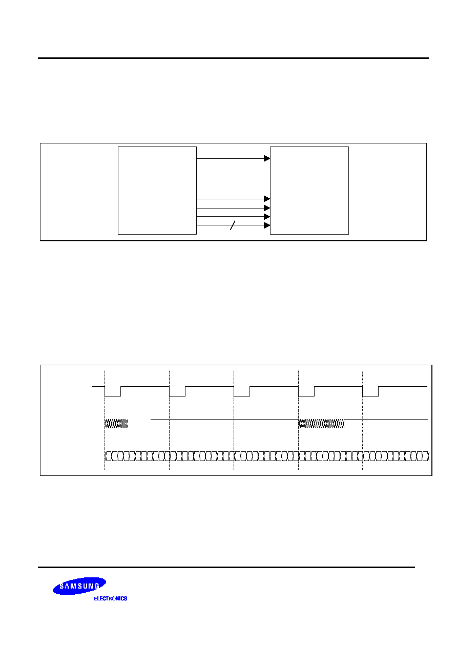
S6D0114 132-RGB X 176-DOT 1-CHIP DRIVER IC FOR 262,144-COLOR TFT-LCD DISPLAY
Preliminary
81
VSYNC INTERFACE
The S6D0114 incorporates VSYNC interface, which enables motion pictures to be displayed with only the
conventional system interface and the frame synchronization signal (VSYNC). This interface requires minimal
changes from the conventional system to display motion pictures.
LCDC
/MPU
S6D0114
VSYNC
CSB
RS
/WR
DB17-10, 8-1
16
Figure 49. VSYNC Interface
When DM1-0="10" and RM="0", VSYNC interface is available. In this interface the internal display operation is
synchronized with VSYNC. Data for display is written to RAM via the system interface with higher speed than for
internal display operation. This method enables flicker-free display of motion pictures with the conventional
interface.
Display operation can be achieved by using the internal clock generated by the internal oscillator and the VSYNC
input. Because all the data for display is written to RAM, only the data to be rewritten is transferred. This method
reduces the amount of data transferred during motion picture display operation.
The higher-speed write mode (HWM="1") achieves both low power consumption and high-speed access.
Writing to screen
Writing to screen
VSYNC
GRAM data write
via system interface
Displaying operation in
synchronization with the
Internal clock
Figure 50. Moving Picture Data Transfer via VSYNC Interface
VSYNC interface requires taking the minimum speed for RAM writing via the system interface and the frequency of
the internal clock into consideration. RAM writing should be performed with higher speed than the result obtained
from the calculation shown below.

132-RGB X 176-DOT 1-CHIP DRIVER IC FOR 262,144-COLOR TFT-LCD DISPLAY
S6D0114
Preliminary
82
-------------------------------------------------------------------------------------------------------------------------------------------------------
Internal clock frequency (fosc) [Hz] = Frame freq.
�
(Display raster-row (NL) + Front porch (FP) + Back porch (BP))
�
16-Clock
�
Fluctuation
Minimum speed for RAM writing [Hz] > 176
�
Display raster-row (NL)
/ {((Back porch (BP) + Display raster-row (NL) � Margin)
�
16 Clock) / fosc}
NOTE: When RAM writing does not start immediately after the falling edge of VSYNC, the time between the falling edge of VSYNC and the RAM
writing start timing must also be considered.
-------------------------------------------------------------------------------------------------------------------------------------------------------
An example is shown below.
Example
Display size
132RGB
�
176 raster-rows
Display line number
176 raster-row (NL=10101)
Back/Front porch
3/5 raster-rows (BP=0011/FP=0101)
Frame Frequency
60Hz
Internal clock frequency (fosc) [Hz]= 60 Hz
�
(176 + 2 + 14)
�
16 clock
�
1.1 / 0.9 = 216 kHz
NOTES:
1. Calculating the internal clock frequency requires considering the fluctuation. In the above case a 10%
Fluctuation within the VSYNC period is assumed.
2. The fluctuation includes LSI production variation and air temperature fluctuation. Other fluctuations,
including those for the external resistors and the supplied power, are not included in this example. Please keep in mind that a
margin for these factors is also needed.
Minimum speed for RAM writing [Hz] > 132
�
176 / {((3 + 176 � 5) raster-rows
�
16 clock) / 216kHz} = 1.8 MHz
NOTES:
3. In this case RAM writing starts immediately after the falling edge of VSYNC.
4. The margin for display raster-row should be two raster-rows or more at the completion of RAM writing
for one frame.
Therefore, when RAM writing starting immediately after the falling edge of VSYNC is performed at 1.8 MHz or more,
the data for display can be rewritten before display operation starts. This means that flicker-free display operation is
achieved.
Display
(176-line)
Blanking period
Back porch (5-line)
Front porch (3-line)
RAM
write
Displaying
operation
VSYNC
[Line]
176
0
executed
line
2.32
12.90
13.04
16.74
(60Hz)
Back porch
14H
VSYNC
RAM write(10MHz)
23232 times
RAM write
1.8MHz
Displaying
operation
RC oscillation
�
10%
Displaying
operation
Figure 51. Operation for VSYNC Interface

S6D0114 132-RGB X 176-DOT 1-CHIP DRIVER IC FOR 262,144-COLOR TFT-LCD DISPLAY
Preliminary
83
Usage on VSYNC interface
1. The Example above is a calculated value. Please keep in mind that a margin for these factors is also
needed. Because production variation of the internal oscillator requires consideration.
2. The Example above is a calculated value of rewriting the whole screen. A limitation of the motion picture
area generates a margin for the RAM write speed.
(20-line)
(20-line)
Moving picture
display
(200-line)
Example: moving picture display area(20~156-line)
Back porch (3-line)
Front porch (5-line)
RAM
write
[Line]
176
0
executed
line
16.74
(60Hz)
[ms]
Back porch
14H
VSYNC
RAM write
1.8MHz
Displaying
operation
RC oscillation
�
10%
Displaying
operation
156
9.97
13.04
20
Figure 52. Limitation of Motion picture Area
3. During the period between the completion of displaying one frame data and the next VSYNC signal, the
display will remain front porch period.
4. Transition between the internal operating clock mode (DM1-0="00") and VSYNC interface mode will be
valid after the completion of the screen, which is displayed when the instruction is set.

132-RGB X 176-DOT 1-CHIP DRIVER IC FOR 262,144-COLOR TFT-LCD DISPLAY
S6D0114
Preliminary
84
HWM=1, AM=0
Address setting
VSYNC interface mode setting
(DM1-0=10, RM=0)
Index register setting(R22h)
Wait more than 1 frame
VSYNC interface
RAM data writing
VSYNC interface
Operation
Internal clock mode setting
(DM1-0=00, RM=0)
Wait more than 1 frame
Internal clock operation
Internal clock operation
Display operation in
synchronization with
the internal clock
The value set in DM1-
0 and RM will be valid
after completion of 1-
frame display.
Display operation in
synchronization with
VSYNC
Note: When the interface mode is switched,
VSYNC should be input before setting
DM1-0 and RM bit.
Internal clock operation =>VSYNC interface
Wait more than 1 frame
Internal clock mode setting
(DM1-0=00, RM=0)
Internal clock operation
VSYNC interface operation
Display operation in
synchronization with
VSYNC
The value set in DM1-
0 and RM will be valid
after completion of 1-
frame display.
Display operation in
synchronization with
the internal clock
Note: When switching to internal clock mode,
Please keep supplying VSYNC signal for
more than 1 frame.
VSYNC interface => Internal clock operation
Figure 53. Transition between the Internal Operating Clock Mode and VSYNC Interface Mode
5. Partial display, vertical scroll, and interlaced driving functions are not available on VSYNC interface mode.
6. The VSYNC interface is performed by the method above, therefore, AM bit should be 0.
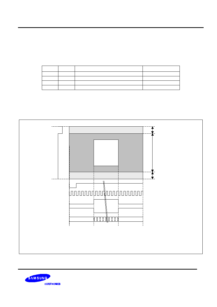
S6D0114 132-RGB X 176-DOT 1-CHIP DRIVER IC FOR 262,144-COLOR TFT-LCD DISPLAY
Preliminary
85
EXTERNAL DISPLAY INTERFACE
The following interfaces are available as external display interface. It is determined by bit setting of RIM1-0. RAM
accesses can be performed via the RGB interface.
Table 28. RIM Bits
RIM1
RIM0
RGB Interface
PD Pin
0
0
18-bit RGB interface
PD17 to 0
0
1
16-bit RGB interface
PD17 to13, 11 to 1
1
0
6-bit RGB interface
PD17 to12
1
1
Setting disabled
RGB INTERFACE
The RGB interface is performed in synchronization with VSYNC, HSYNC, and DOTCLK. Combining the function of
the high-speed write mode and the window address enables transfer only the screen to be updated and reduce the
power consumption.
Moving
picture
display
area
Moving
picture
display
area
RAM data display area
VSYNC
Back porch period
Front porch period
Display period (NL4-0)
HSYNC
DOTCLK
ENABLE
VLD
PD17-0
VSYNC : Frame synchronized signal
HSYNC : Line synchronized signal
DOTCLK : Dot clock
ENABLE : Data enable signal
VLD : Valid data signal
PD17-0 : RGB(6:6:6) display data
Back porch period(BPP) : 14H
BP3-0
2H
Front porch period(FPP) : 14H
FP3-0
2H
FPP+BPP=16H
Display period(DP) : NL4-0
176H
A number of line of 1-frame : FPP+DP+BPP
Figure 54. RGB Interface
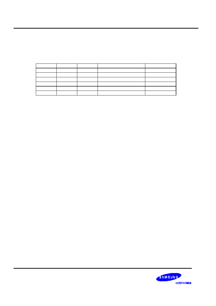
132-RGB X 176-DOT 1-CHIP DRIVER IC FOR 262,144-COLOR TFT-LCD DISPLAY
S6D0114
Preliminary
86
VLD AND ENABLE SIGNALS
The relationship between VLD and ENABLE signals is shown below. When ENABLE is active, the address is not
updates. When VLD is active and ENABLE is active, the address is updated.
Table 29. Relationship between VLD and ENABLE
EPL
ENABLE
VLD
RAM WRITE
RAM ADDRESS
0
0
0
Valid
Updated
0
0
1
Invalid
Updated
0
1
*
Invalid
Hold
1
0
*
Invalid
Hold
1
1
0
Valid
Update
1
1
1
Invalid
Updated
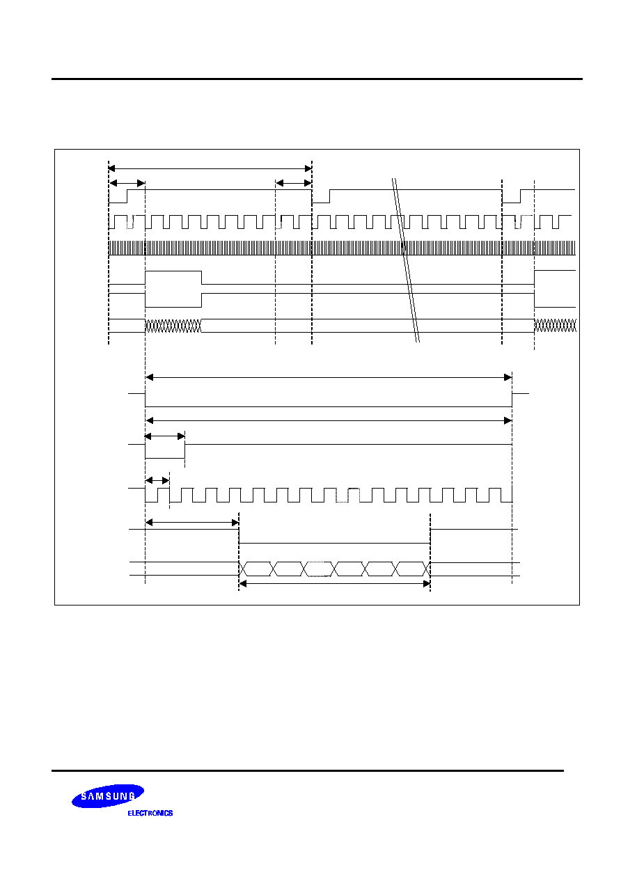
S6D0114 132-RGB X 176-DOT 1-CHIP DRIVER IC FOR 262,144-COLOR TFT-LCD DISPLAY
Preliminary
87
RGB INTERFACE TIMING
Time chart for RGB interface is shown below.
VSYNC
HSYNC
DOTCLK
ENABLE
PD17-0
1-frame
Back porch period
Front porch period
1H
HLW
1CLK
1CLK
DTST
HLW
VSYNC
HSYNC
DOTCLK
ENABLE
VLD
PD17-0
Valid data
1H
VLD
Figure 55. 16-/18-bit RGB Interface Timing
VLW: The period in which VSYNC is "Low" level
HLW: The period in which HSYNC is "Low" level
DTST: Set up time of data transfer
NOTE: Data for display should be written in the high-speed write mode (HWM="1") in VSYNC is in use.
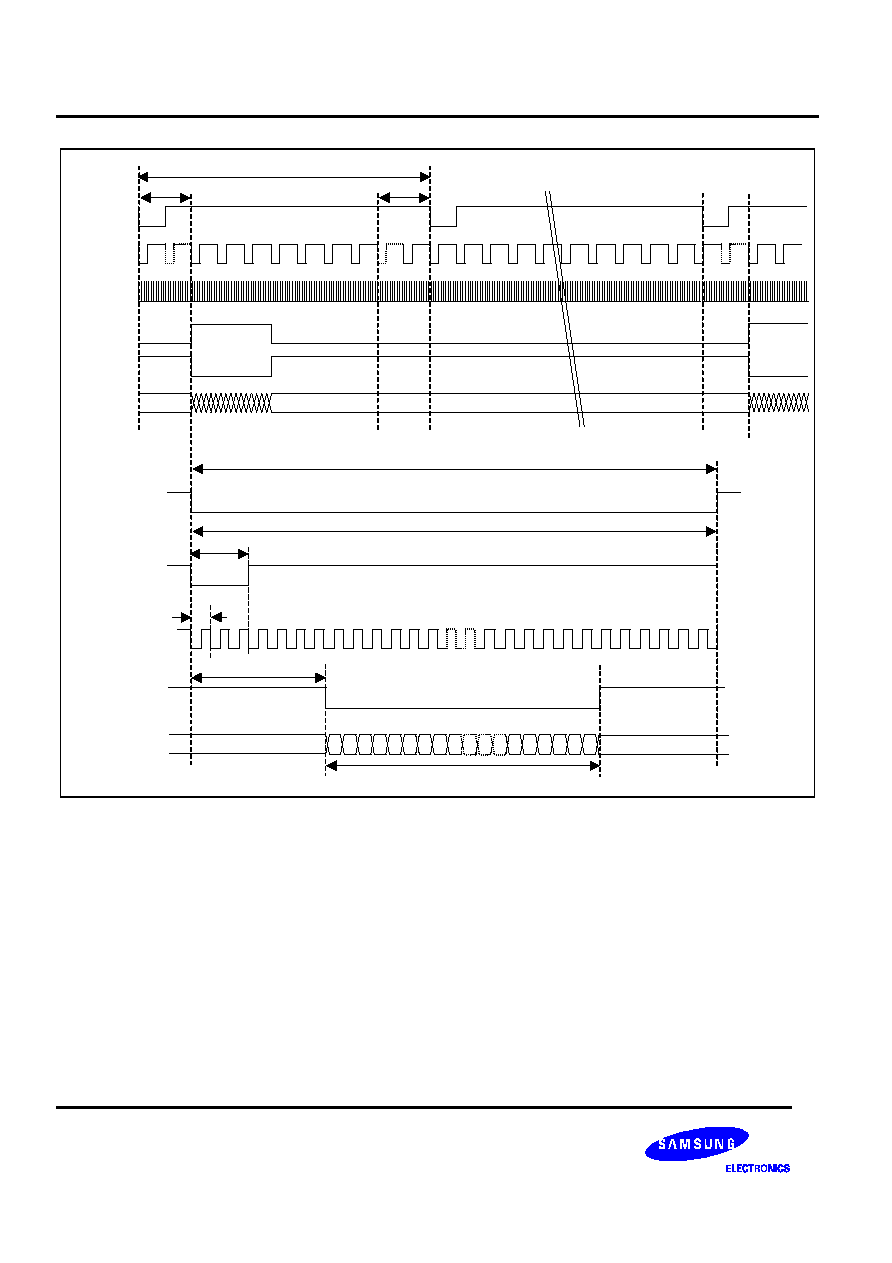
132-RGB X 176-DOT 1-CHIP DRIVER IC FOR 262,144-COLOR TFT-LCD DISPLAY
S6D0114
Preliminary
88
1H
HLW
3CLK
1CLK
DTST
HLW
VSYNC
HSYNC
DOTCLK
ENABLE
VLD
PD17-0
Valid data
1H
R G B R G B R G B R G B R G B
VSYNC
HSYNC
DOTCLK
ENABLE
PD17-0
1-frame
Back porch period
Front porch period
VLD
Figure 56. 6-bit RGB Interface Timing
VLW: The period in which VSYNC is "Low" level
HLW: The period in which HSYNC is "Low" level
DTST: Set up time of data transfer
NOTES:
1. Three clocks are regarded as one clock for transfer when data is transferred in 6-bit interface.
2. VSYNC, HSYNC, ENABLE, DOTCLK, VLD, and PD17-2 should be transferred in units of three clocks.
3. Data for display should be written in the high-speed write mode (HWM="1") in VSYNC interface is in
use.
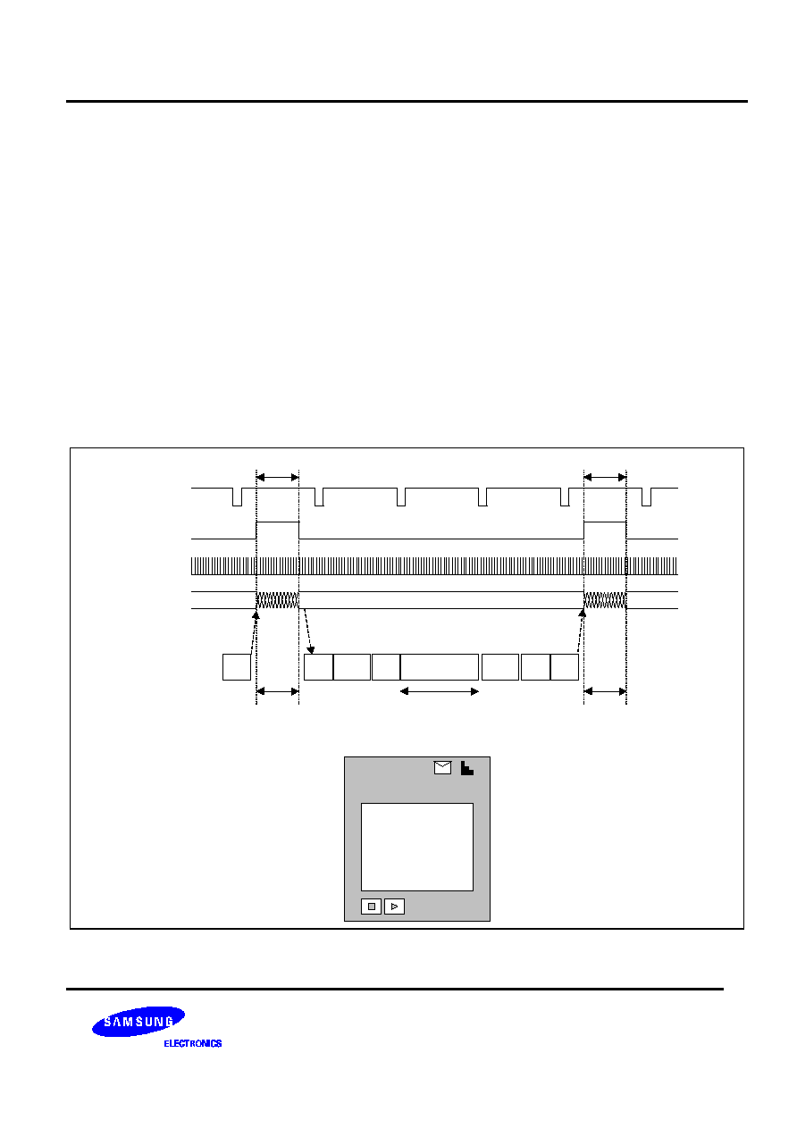
S6D0114 132-RGB X 176-DOT 1-CHIP DRIVER IC FOR 262,144-COLOR TFT-LCD DISPLAY
Preliminary
89
MOVING PICTURE DISPLAY
The S6D0114 incorporates RGB interface to display motion pictures and RAM to store data for display.
For displaying motion pictures, the S6D0114 has the following features.
- Motion picture area can only be transferred by the window address function.
- The high-speed write mode achieves both low power consumption and high-speed access.
- Motion picture area to be rewritten can only be transferred.
- Reducing the amount of data transferred enables reduce the power consumption to the whole system.
- Still picture area, such as an icon, can be updated while displaying motion pictures combining with the system
interface.
RAM ACCESS VIA RGB INTERFACE AND SYSTEM INTERFACE
RAM can be accessed via the system interface when RGB interface is in use. When data is written to RAM during
RGB interface mode, the ENABLE bit should be low to stop data writing via RGB interface, because RAM writing is
always performed in synchronization with the DOTCLK input when ENABLE is high. After this RAM access via the
system interface, a waiting time is needed for a write/read bus cycle before the next RAM access starts via RGB
interface. When a RAM write conflict occurs, data writing is not guaranteed.
Example of display motion picture via RGB-I/F and updating still picture via the system interface are shown below.
VSYNC
ENABLE
DOTCLK
PD17-0
System
interface
RM=0
Index
R22
Address
set
Index
R22
Writing display data
except moving picture
display area
RM=1
Address
set
Index
R22
Moving picture
display area
2002/01/14 00:00
Still picture display area
Writing moving picture
display area
Writing moving picture
display area
Index set
Writing picture
Writing picture
Writing still picture
display area
Figure 57. Example of Updating Still Picture Area during Displaying Motion Picture
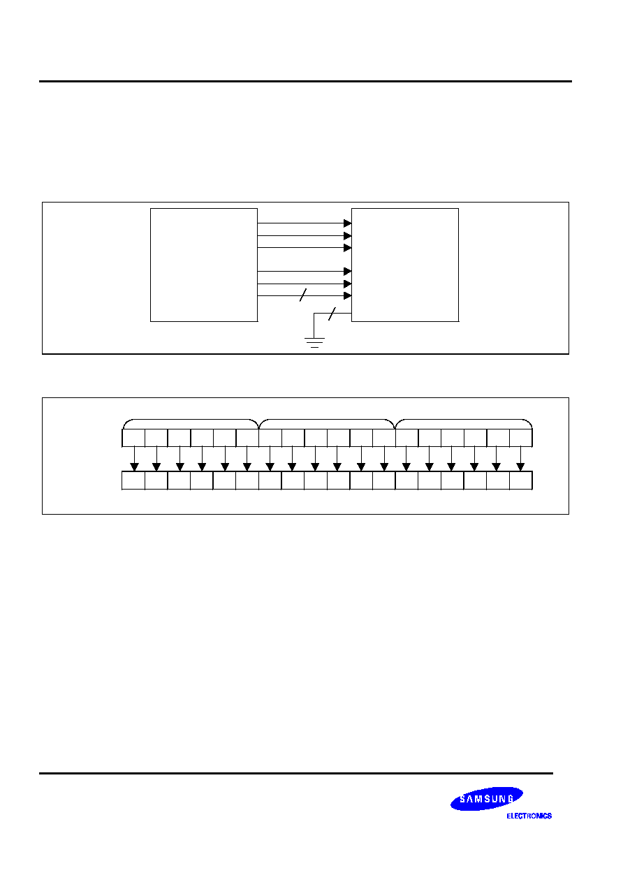
132-RGB X 176-DOT 1-CHIP DRIVER IC FOR 262,144-COLOR TFT-LCD DISPLAY
S6D0114
Preliminary
90
6-BIT RGB INTERFACE
6-bit RGB interface can be used by setting RIM1-0 pins to "00". Display operation is synchronized with VSYNC,
HSYNC, and DOTCLK signals. Data for display is transferred to the internal RAM via 6-bit RGB data bus (PD17 to
12), the data valid signal (VLD), and the data enable signal (ENABLE). Unused pins must be fixed to the VDD3 or
GND level.
LCDC
S6D0114
VSYNC
HSYNC
DOTCLK
VLD
ENABLE
PD17-12
6
12
Figure 58. 6-bit RGB Interface
R5
R4
R3
R2
R1
R0
G5
G4
G3
G2
G1
G0
B5
B4
B3
B2
B1
B0
1-pixel
PD
17
PD
16
PD
15
PD
14
PD
13
PD
12
PD
17
PD
16
PD
15
PD
14
PD
13
PD
12
PD
17
PD
16
PD
15
PD
14
PD
13
PD
12
1st transfer
2nd transfer
3rd transfer
*262,144-color display is available in the 6-bit RGB interface
Input
GRAM write data
Figure 59. GRAM Write Data format for 6-bit RGB Interface Mode
NOTE: Transfer synchronization function for an 6-bit bus interface. The S6D0114 has the transfer counter to count 1st, 2nd and 3rd data transfer
in the 6-bit bus interface. The transfer counter is reset on the falling edge of VSYNC and enters the 1st data transmission state. Transfer
mismatch can be corrected transfer restarts correctly. In this method, when data is consecutively transferred such as displaying motion pictures,
the effect of transfer mismatch will be reduced and recover normal operation.
NOTE: The internal display is operated in units of three DOTCLK. When the DOTCLK is not input in units of pixels, click mismatch occurs and the
frame, which is operated, and the next frame are not display correctly.
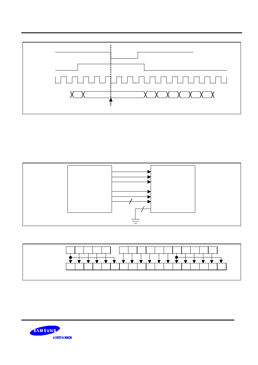
S6D0114 132-RGB X 176-DOT 1-CHIP DRIVER IC FOR 262,144-COLOR TFT-LCD DISPLAY
Preliminary
91
Transfer sync.
2nd
transfer
2nd
transfer
1st
transfer
3rd
transfer
1st
transfer
2nd
transfer
3rd
transfer
VSYNC
ENABLE
DOTCLK
PD17-0
Transfer sync.
2nd
transfer
2nd
transfer
1st
transfer
3rd
transfer
1st
transfer
2nd
transfer
3rd
transfer
VSYNC
ENABLE
DOTCLK
PD17-0
Figure 60. Transfer Synchronization Function when 6-bit RGB Interface
16-BIT RGB INTERFACE
16-bit RGB interface can be used by setting RIM1-0 pins to 01. Display operation is synchronized with VSYNC,
HSYNC, and DOTCLK signals. Data for display is transferred to the internal RAM via 6-bit RGB data bus (PD17-13
and 11-1), The data valid signal (VLD). Instruction should be set via the system interface.
LCDC
S6D0114
VSYNC
HSYNC
DOTCLK
VLD
ENABLE
PD17-13, 11-1
16
2
Figure 61. 16-bit RGB Interface to System
R5
R4
R3
R2
R1
R0
G5
G4
G3
G2
G1
G0
B5
B4
B3
B2
B1
B0
Input
GRAM write data
PD
17
PD
16
PD
15
PD
14
PD
13
PD
11
PD
10
PD
9
PD
8
PD
7
PD
6
PD
5
PD
4
PD
3
PD
2
PD
1
1-pixel
R5
R4
R3
R2
R1
R0
G5
G4
G3
G2
G1
G0
B5
B4
B3
B2
B1
B0
Input
GRAM write data
PD
17
PD
16
PD
15
PD
14
PD
13
PD
11
PD
10
PD
9
PD
8
PD
7
PD
6
PD
5
PD
4
PD
3
PD
2
PD
1
1-pixel
Figure 62. GRAM Write Data in the 16-bit RGB Interface Mode
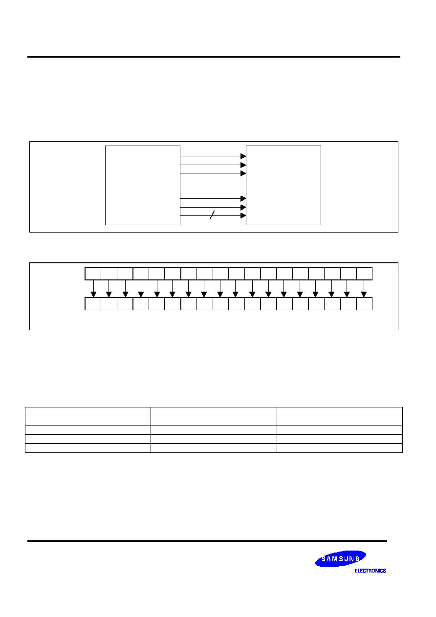
132-RGB X 176-DOT 1-CHIP DRIVER IC FOR 262,144-COLOR TFT-LCD DISPLAY
S6D0114
Preliminary
92
18-BIT RGB INTERFACE
18-bit RGB interface can be used by setting MIF1-0 pins to 01. Display operation is synchronized with VSYNC,
HSYNC, and DOTCLK signals. Data for display is transferred to the internal RAM via 6-bit RGB data bus (PD17-0),
the data valid signal (VLD).
LCDC
S6D0114
VSYNC
HSYNC
DOTCLK
VLD
ENABLE
PD17-13, 11-1
18
Figure 63. 18-bit RGB Interface to System
Input
PD
17
PD
16
PD
15
PD
14
PD
13
PD
12
PD
11
PD
10
PD
9
PD
8
PD
7
PD
6
PD
5
PD
4
PD
3
PD
2
PD
1
PD
0
R5
R4
R3
R2
R1
R0
G5
G4
G3
G2
G1
G0
B5
B4
B3
B2
B1
B0
GRAM write data
*262,144-color display is available in the 18-bit RGB interface
1-pixel
Figure 64. GRAM Write Data format for 18-bit RGB Interface Mode
USAGE ON EXTERNAL DISPLAY INTERFACE
1. When external display interface is in use, the following functions are not available.
Table 30. External Display Interface and Internal Display Operation
Function
External Display Interface
Internal Display Operation
Partial Display
Cannot be used
Can be used
Scroll Function
Cannot be used
Can be used
Interlaced Driving
Cannot be used
Can be used
Graphics Operation Function
Cannot be used
Can be used
2. VSYNC, HSYNC, and DOTCLK signals should be supplied during display operation via RGB interface.
3. Please make sure that when setting bits of NO1-0, SDT1-0, and EQ1-0 in RGB interface, the clock on which
operations are based changes from the internal operating clock to DCLK.
4. RGB data are transferred for three clock cycles in 6-bit RGB interface. Data transferred, therefore, should be
transferred in units of RGB.

S6D0114 132-RGB X 176-DOT 1-CHIP DRIVER IC FOR 262,144-COLOR TFT-LCD DISPLAY
Preliminary
93
5. Interface signals, VSYNC, HSYNC, DOTCL, ENABLE, VLD, and PD17-0 should be set in units of RGB (pixels) to
match RGB transfer.
6. Transitions between internal operation mode and external display interface should follow the mode transition
sequence shown below.
7. During the period between the completion of displaying one frame data and the next VSYNC signal, the display
will remain front porch period.
8. RGB interface should be used in high-speed write mode (HWM="1").
9. An address set is done on the falling edge of VSYNC every frame in RGB interface.
HWM=1, AM=0
Address setting
RGB interface mode setting
(DM1-0=01, RM=1)
Index register setting(R22h)
Wait more than 1 frame
RGB interface
RAM data writing
VSYNC interface
Operation
Internal clock operation
Display operation in
synchronization with
the internal clock
The value set in DM1-
0 and RM will be valid
after completion of 1-
frame display.
Display operation in
synchronization with
RGB signal
Note: When the interface mode is switched,
VSYNC, HSYNC, DOTCLK and ENABLE
should be input before setting DM1-0 and
RM bit.
Internal clock operation =>RGB interface(1)
Wait more than 1 frame
Internal clock mode setting
(DM1-0=00, RM=0)
Internal clock operation
RGB interface operation
Display operation in
synchronization with
the RGB signal
The value set in DM1-
0 and RM will be valid
after completion of 1-
frame display.
Display operation in
synchronization with
the internal clock
Note: When switching to RGB interface,
Please input RGB interface signal(VSYNC,
HSYNC, DOTCLK, ENABLE) before DM1-0,
RM bit setting.
RGB Interface (1) => Internal clock operation
Figure 65. Transition between the Internal Operating Clock Mode and RGB Interface Mode

132-RGB X 176-DOT 1-CHIP DRIVER IC FOR 262,144-COLOR TFT-LCD DISPLAY
S6D0114
Preliminary
94
HIGH-SPEED BURST RAM WRITE FUNCTION
The S6D0114 has a high-speed burst RAM-write function that can be used to write data to RAM in one-fourth the
access time required for an equivalent standard RAM-write operation. This function is especially suitable for
applications that require the high-speed rewriting of the display data, for example, display of color animations, etc.
When the high-speed RAM-write mode (HWM) is selected, data for writing to RAM is once stored to the S6D0114
internal register. When data is selected four times per word, all data is written to the on-chip RAM. While this is
taking place, the next data can be written to an internal register so that high-speed and consecutive RAM writing can
be executed for animated displays, etc.
Microcomputer
Register 1
Register 2
Register 3
Register 4
18
72
"0000"H
"0001"H
"0002"H
"0003"H
GRAM
Address
counter
(AC)
16
a) High-speed burst RAM write operation flow
CSB
(input)
b) Example of the operation of high-speed consecutive writing to RAM
1 2 3 4 1 2 3 4 1 2 3 4
Index
(R22)
RAM
data
1
RAM
data
2
RAM
data
3
RAM
data
4
RAM
data
5
RAM
data
6
RAM
data
7
RAM
data
8
RAM
data
9
RAM
data
10
RAM
data
11
RAM
data
12
Index
RAM write
execution time
RAM write
execution time
RAM write
execution time*
RAM
data 1 to 4
RAM
data 5 to 8
RAM
data 9 to 12
E
(input)
DB17-0
(input/output)
RAM write data
(72 bit)
RAM address
(AC 15-0)
"0000"H
"0004"H
"0008"H
"000A"H
NOTE: The lower two bits of the address must be set in the following way in high-speed write mode.
ID0=0: The lower 2 bits of the address must be set to 11.
ID0=1: The lower 2 bits of the address must be set to 00.
When a high speed RAM write is canceled, the next instruction must only be executed
after the RAM write execution time has elapsed.
Figure 66. Example of the operation of high-speed consecutive writing to RAM
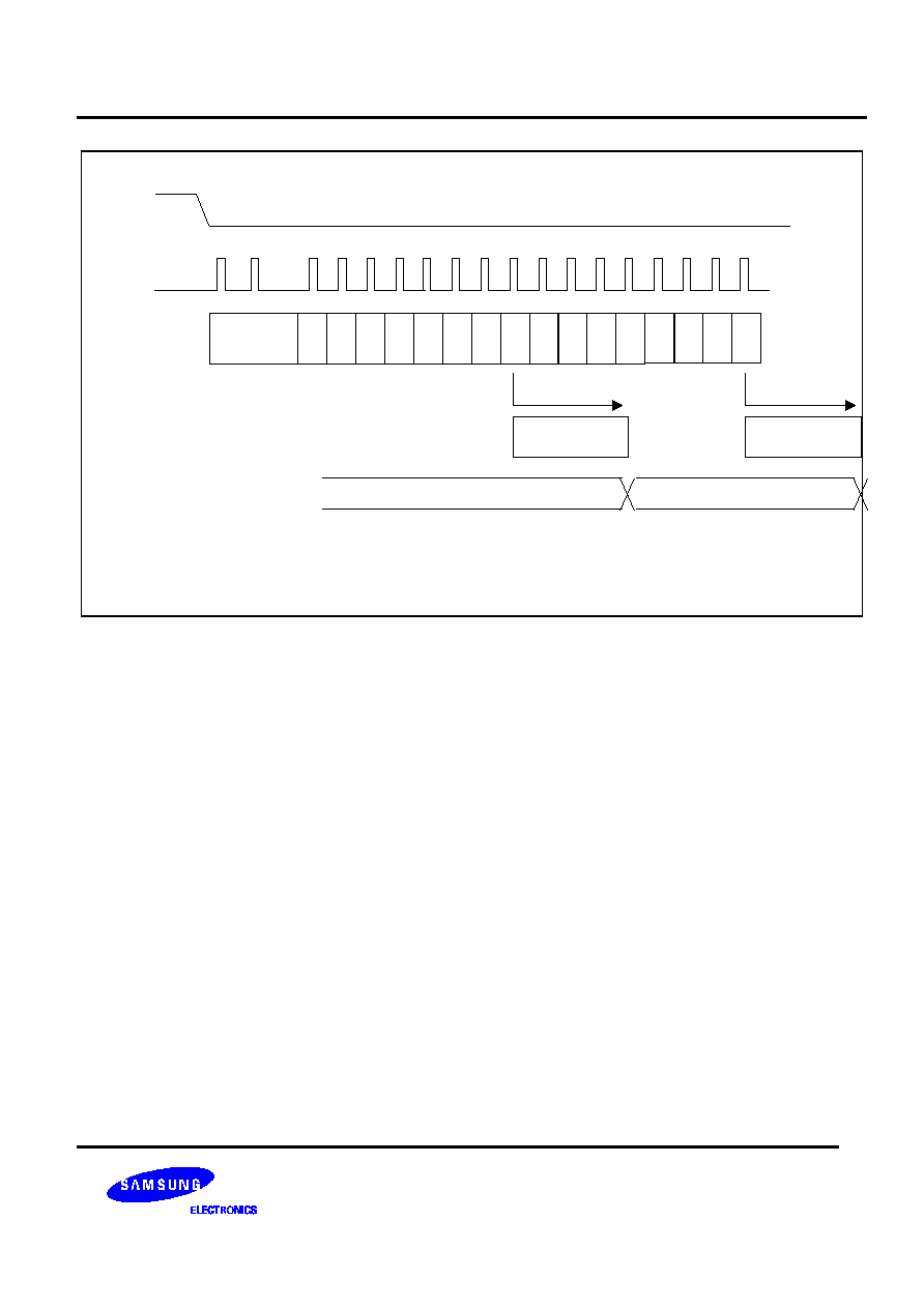
S6D0114 132-RGB X 176-DOT 1-CHIP DRIVER IC FOR 262,144-COLOR TFT-LCD DISPLAY
Preliminary
95
CSB
(input)
c) Example of the operation of high-speed consecutive writing to RAM (when 8-bit interface is used)
1 2 3 4 5 6 7 8 1 2 3 4 5 6 7 8
E
(input)
Index
(R22)
RAM
data
1
upper
RAM
data
1
lower
RAM
data
2
upper
RAM
data
2
lower
RAM
data
3
upper
RAM
data
3
lower
RAM
data
4
upper
RAM
data
4
lower
RAM
data
1
upper
RAM
data
1
lower
RAM
data
2
upper
RAM
data
2
lower
DB15-0
(input/output)
RAM
data
3
upper
RAM
data
3
lower
RAM
data
4
upper
RAM
data
4
lower
RAM write
execution time
RAM write
execution time
RAM write data
(64 bits)
RAM
data 1 to 4
RAM
data 5 to 8
RAM address
(AC 15-0)
"0000"H
"0004"H
NOTE: The lower two bits of the address must be set in the following way in high-speed write mode.
ID0=0: The lower 2 bits of the address must be set to 11.
ID0=1: The lower 2 bits of the address must be set to 00.
Writing is executed every 4 words in the high speed RAM write mode. Therefore, MM writing is executed
every 8 writing operations when 8-bit interface is used.
Figure 67. Example of the operation of high-speed consecutive writing to RAM (8-bit interface)

132-RGB X 176-DOT 1-CHIP DRIVER IC FOR 262,144-COLOR TFT-LCD DISPLAY
S6D0114
Preliminary
96
When high-speed write mode is used, note the following.
1. The logical and compare operations cannot be used.
2. Data is written to RAM each four words. When an address is set, the lower two bits in the address must be set to
the following values.
*When ID0=0, the lower two bits in the address must be set to 11 and be written to RAM.
*When ID0=1, the lower two bits in the address must be set to 00 and be written to RAM.
3. Data is written to RAM each four words. If less than four words of data is written to RAM, the last data will not be
written to RAM.
4. When the index register and RAM data write (R22h) have been selected, the data is always written first. RAM
cannot be written to and read from at the same time. HWM must be set to 0 while RAM is being read.
5. High-speed and normal RAM write operations cannot be executed at the same time. The mode must be switched
and the address must then be set.
6. When high-speed RAM write is used with a window address-range specified, dummy write operation may be
required to suit the window address range-specification. Refer to the High-Speed RAM Write in the Window Address
section.
Table 31. Comparison between Normal and High-speed RAM Write Operations
Normal RAM Write
(HWM=0)
High-speed RAM Write
(HWM=1)
Logical operation function
Can be used
Cannot be used
Compare operation function
Can be used
Cannot be used
BGR function (RGB swap)
Can be used
Can be used
Write mask function
Can be used
Can be used
RAM address set
Can be specified by word
ID0 bit=0: Set the lower two bits to 11
ID0 bit=1: Set the lower two bits to 00
RAM read
Can be read by word
Cannot be used
RAM write
Can be written by word
Dummy write operations may have to
be inserted according to a window
address-range specification
Window address
Can be set by word
The horizontal range(HAS/HSE):
More than four words
The number of horizontal writing:
4N(N 2)
External display interface
Can be used
Can be used
AM setting
AM=1/0
AM=0
NOTE: 1 word = 2 byte.
S6D0114 132-RGB X 176-DOT 1-CHIP DRIVER IC FOR 262,144-COLOR TFT-LCD DISPLAY
Preliminary
97
HIGH-SPEED RAM WRITE IN THE WINDOW ADDRESS
When a window address range is specified, GRAM data that is in an optional window area can be updated quickly
and continuously by use of dummy write operation. So that the number of RAM access become 4N as shown in the
table below.
Dummy write operation must be inserted at the first or last of a row of data, depending on the horizontal window-
address range specification bits (HSA1 to 0, HEA1 to 0). Numbers of dummy write operations of a row must be 4N.
Table 32. Number of Dummy Write Operations in High-Speed RAM Write (HSA bits)
HSA1
HSA0
Number of dummy write operations to be inserted at the start of a row
0
0
0
0
1
1
1
0
2
1
1
3
Table 33. Table 34. Number of Dummy Write Operations in High-Speed RAM Write (HEA bits)
HEA1
HEA0
Number of dummy write operations to be inserted at the end of a row
0
0
3
0
1
2
1
0
1
1
1
0
NOTE: Each row of access must consist of 4 X N operations, including the dummy writes.
Horizontal access count = first dummy write count + write data count + last dummy write count = 4 X N

132-RGB X 176-DOT 1-CHIP DRIVER IC FOR 262,144-COLOR TFT-LCD DISPLAY
S6D0114
Preliminary
98
An example of high-speed RAM write with a window address-range specified is shown below.
The window address-range can be accessed consecutively and quickly by inserting two dummy writes at the start of
a row and three dummy writes at the end of a row, as determined by using the window address-range specification
bits (HSA1 to 0=10, HEA1 to 0=00).
Writing in the horizontal direction
AM=0, ID0=1
Window address-range setting
HSA=h12, HEA=h30
VSA=h08, VEA=hA0
High-speed RAM write mode
setting HWM=1
Address set
AD=h0810*
Dummy RAM write X 2
RAM write X 31
Dummy RAM write X 3
X 153
h0000
hAF83
Window address
range specification
(rewritable area)
h0812
hA030
Window address-range setting
HSA=h12, HEA=h30
VSA=h08, VEA=hA0
NOTE: The address set for the high-speed RAM write must be 00 or 11 according to the value of the ID0 bit.
Only pre-specified window address-range will be overwritten.
GRAM address map
Figure 68. Example of High-speed RAM Write with a window address-range specification
S6D0114 132-RGB X 176-DOT 1-CHIP DRIVER IC FOR 262,144-COLOR TFT-LCD DISPLAY
Preliminary
99
WINDOW ADDRESS FUNCTION
When data is written to the on-chip GRAM, a window address-range which is specified by the horizontal address
register (start: HSA7-0, end: HEA 7-0) and vertical address register (start: VSA7-0, end: VEA7-0) can be updated
consecutively
.
Data is written to addresses in the direction specified by the AM and ID1-0bit. When image data, etc. is being written,
data can be written consecutively without thinking a data wrap by doing this.
The window must be specified to be within the GRAM address area described as following example. Addresses
must be set within the window address.
[Restriction on window address-range settings]
(horizontal direction) 00H
HSA7-0
HEA7-0
83H
(vertical direction) 00H
VSA7-0
VEA7-0
AFH
[Restriction on address settings during the window address]
(RAM address) HSA7-0
AD7-0
HEA7-0
VSA7-0
AD15-8
VEA7-0
Note: In high-speed RAM-write mode, the lower two bits of the address must be set as shown below according to the
value of the ID0 bit.
ID0=0: The lower two bits of the address must be set to 11.
ID0=1: The lower two bits of the address must be set to 00.
GRAM address map
"0000"H
"0083"H
"AF00"H
"AF83"H
"2010"H
"2110"H
"5F10"H
"202F"H
"212F"H
"5F2F"H
Window address-range specification area
HSA7-0 = "10"H, HSE7-0 = "2F"H
I/D = 1 (increment)
VSA7-0 = "20"H, VEA7-0 = "5F"H
AM = 0 (horizontal writing)
Figure 69. Example of address operation in the window address specification
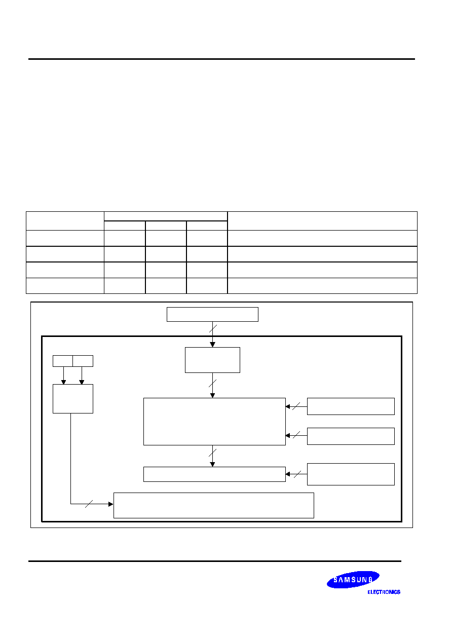
132-RGB X 176-DOT 1-CHIP DRIVER IC FOR 262,144-COLOR TFT-LCD DISPLAY
S6D0114
Preliminary
100
GRAPHICS OPERATION FUNCTION
The S6D0114 can greatly reduce the load of the microcomputer graphics software processing through the 16-bit bus
architecture and internal graphics-bit operation function. This function supports the following:
1. A write data mask function that selectively rewrites some of the bits in the 18-bit write data.
2. A logical operation write function that writes the data sent from the microcomputer and the original
RAM data by a logical operation.
3. A conditional write function that compares the original RAM data or write data and the compare-bit data and
writes the data sent from the microcomputer only when the conditions match.
Even if the display size is large, the display data in the graphics RAM (GRAM) can be quickly rewritten.
The graphics bit operation can be controlled by combining the entry mode register, the bit set value of the RAM-
write-data mask register, and the read/write from the microcomputer.
Table 35. Graphics Operation
Bit setting
Operation mode
I/D
AM
LG2-0
Operation and usage
Write mode 1
0/1
0
000
Horizontal data replacement
Write mode 2
0/1
1
000
Vertical data replacement
Write mode 3
0/1
0
110 111
Conditional horizontal data replacement
Write mode 4
0/1
1
110 111
Conditional vertical data replacement
Microcomputer
Write-data latch
Logical/Compare operation (LG2- 0):
000:replacement,001:OR,010:AND,011:EOR,
110:replacement with matched write,
111:replacement with unmatched write
Logical operation bit (LG2=0)
Compare bit (CP17-0)
Write-mask register
(WM17-0)
Write bit mask
Graphic RAM (GRAM)
Address
counter
(AC)
+1/-1 +256
16
16
18
18
18
18
3
Figure 70. Data processing flow of graphic operation
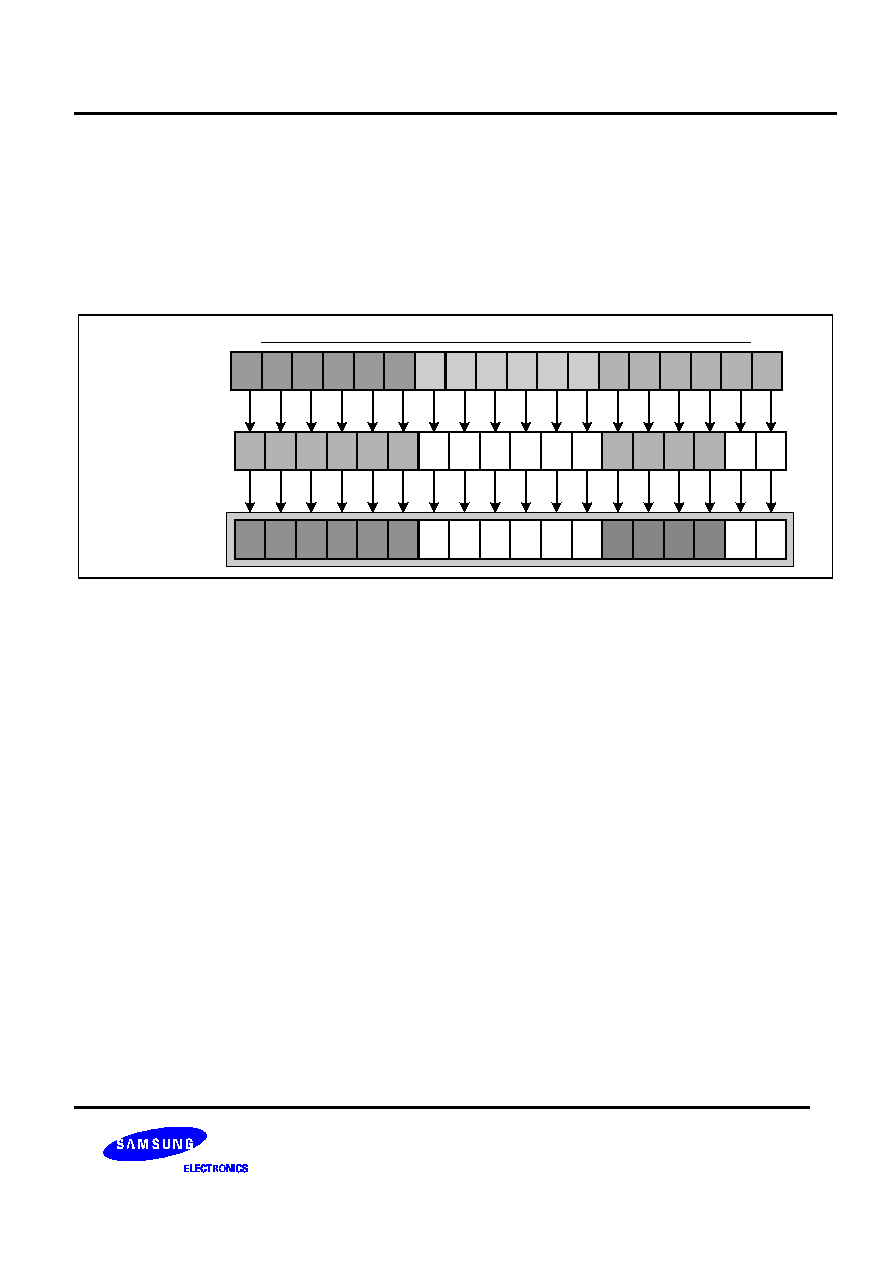
S6D0114 132-RGB X 176-DOT 1-CHIP DRIVER IC FOR 262,144-COLOR TFT-LCD DISPLAY
Preliminary
101
WRITE-DATA MASK FUNCTION
The S6D0114 has a bit-wise write-data mask function that controls writing the two-byte data from the microcomputer
to the GRAM. Bits that are 0 in the write-data mask register (WM17�0) cause the corresponding DB bit to be written
to the GRAM. Bits that are 1 prevent writing to the corresponding GRAM bit to the GRAM; the data in the GRAM is
maintained. This function can be used when only one-pixel data is rewritten or the particular display color is
selectively rewritten.
GRAM DATA
R5
R4
R3
R2
R1
R0
G5
G4
G3
G2
G1
G0
B5
B4
B3
B2
B1
B0
Data written by the
microcomputer
Write data Mask
*
*
*
*
*
*
G5
G4
G3
G2
G1
G0
*
*
*
*
B1
B0
1
R5
DB17
DB0
1
1
1
1
1
0
0
0
0
0
0
1
1
1
1
0
0
0
17
Figure 71. Example of write-data mask function operation
Note: Data is expanded to 18 bits when 16-/8-bit system and 16-bit RGB interface is in use.

132-RGB X 176-DOT 1-CHIP DRIVER IC FOR 262,144-COLOR TFT-LCD DISPLAY
S6D0114
Preliminary
102
GRAPHICS OPERATION PROCESSING
1. Write mode 1: AM = 0, LG2�0 = 000
This mode is used when the data is horizontally written at high speed. It can also be used to initialize the graphics
RAM (GRAM) or to draw borders. The write-data mask function (WM17�0) is also enabled in these operations.
After writing, the address counter (AC) automatically increments by 1 (I/D = 1) or decrements by 1 (I/D = 0), and
automatically jumps to the counter edge one-raster-row below after it has reached the left or right edge of the
GRAM.
WM17
WM0
DB17
DB0
Operation Examples:
1) I/D = "1", AM = "0", LG2-0 = "000"
2) WM17-0 = "007FF'H
3) AC = "0000"H
Write data mask:
Write data (1):
Write data (2):
"0000"H
"0001"H
"0002"H
Write data (1)
Write data (2)
GRAM
NOTE: The bits in the GRAM, * 's, are not changed
0
0
0
0
0
0
1
1
1
1
1
1
1
1
1
1
1
1
1
0
0
1
1
1
1
1
1
1
0
0
1
0
1
0
0
0
1
1
0
0
0
1
0
0
0
0
0
1
1
0
0
0
0
0
1
0
0
1
1
1
* * * * * * * * * * * *
1
1
0
0
0
1
* * * * * * * * * * * *
NOTE: When 8/16-bit system interface or 16-bit RGB interface is used,
the data is expanded to internal 18-bit.
NOTE: <G><B> frame write mask
Figure 72. Writing operation of write mode 1
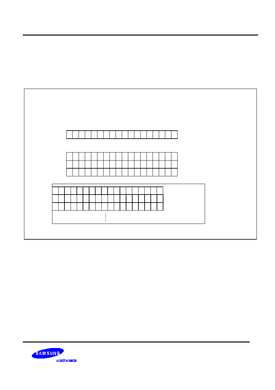
S6D0114 132-RGB X 176-DOT 1-CHIP DRIVER IC FOR 262,144-COLOR TFT-LCD DISPLAY
Preliminary
103
2. Write mode 2: AM = 1, LG2-0 = 000
This mode is used when the data is vertically written at high speed. It can also be used to initialize the GRAM,
develop the font pattern in the vertical direction, or draw borders. The write-data mask function (WM17�0) is also
enabled in these operations. After writing, the address counter (AC) automatically increments by 256, and
automatically jumps to the upper-right edge (I/D = 1) or upper-left edge (I/D = 0) following the I/D bit after it has
reached the lower edge of the GRAM.
Operation Examples:
1) I/D = "1", AM = "1", LG2-0 = "000"
2) WM17-0 = "007FF'H
3) AC = "0000"H
Write data mask:
Write data (1):
Write data (2):
"0000"H
"0100"H
"0200"H
Write data (1)
Write data (2)
GRAM
Write data (3)
Write data (3):
NOTE: 1. The bits in the GRAM, * `s, are not changed.
2. After writing to address "AF00"H, the AC jumps to "0001"H
WM17
WM0
DB17
DB0
0
0
0
0
0
0
1
1
1
1
1
1
1
1
1
1
1
1
1
0
0
1
1
1
1
1
1
1
0
0
1
0
1
0
0
0
1
1
0
0
0
1
0
0
0
0
0
1
1
0
0
0
0
0
0
1
1
1
1
0
1
0
0
0
1
0
0
0
0
0
1
1
1
0
0
1
1
1
* * * * * * * * * * * *
1
1
0
0
0
1
* * * * * * * * * * * *
0
1
1
1
1
0
* * * * * * * * * * * *
NOTE: When 8/16-bit system interface or 16-
bit RGB interface is used,
the data is expanded to internal 18-bit.
Figure 73. Writing operation of write mode 2
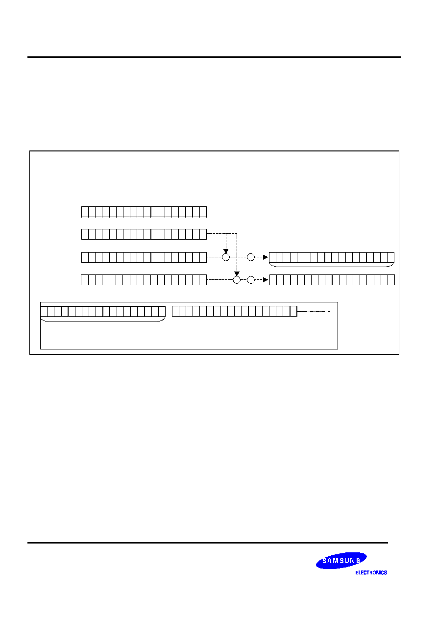
132-RGB X 176-DOT 1-CHIP DRIVER IC FOR 262,144-COLOR TFT-LCD DISPLAY
S6D0114
Preliminary
104
3. Write mode 3: AM = 0, LG2-0 = 110/111
This mode is used when the data is horizontally written by comparing the write data and the set value of the
compare register (CP15�0). When the result of the comparison in a byte unit satisfies the condition, the write data
sent from the microcomputer is written to the GRAM. In this operation, the write-data mask function (WM15�0) is
also enabled. After writing, the address counter (AC) automatically increments by 1 (I/D = 1) or decrements by 1
(I/D = 0), and automatically jumps to the counter edge one-raster-row below after it has reached the left or right
edge of the GRAM.
Operation Examples:
1) I/D = "1", AM = "0", LG2-0 = "110"
2) CP15-0 = "02860"H
3) WM15-0 = "00000"H
4) AC = "0000"H
Write data mask:
WM17
WM0
Compare register:
CP17
CP0
Write data (1):
Write data (2):
DB17
DB0
DB17
DB0
(Matched)
(Unmatched)
C
R
C
R
Compare
operation
Compare
operation
Conditional
replacement
Conditional
replacement
Replacement
"0000"H
"0001"H
GRAM
Matched replacement of write data (1)
0 0 0 0 0 0 0 0 0 0 0 0 0 0 0 0 0 0
* * * * * * * * * * * * * * * * * *
0 0 0 0 0 0 1 1 1 1 1 1 0 0 0 0 0 0
* * * * * * * * * * * * * * * * * *
0 0 1 0 1 0 0 0 0 0 1 1 0 0 0 0 0 0
0 0 1 0 1 0 0 0 0 0 1 1 0 0 0 0 0 0
0 0 1 0 1 0 0 0 0 0 1 1 0 0 0 0 0 0
0 0 1 0 1 0 0 0 0 0 1 1 0 0 0 0 0 0
Figure 74. Writing operation write mode 3

S6D0114 132-RGB X 176-DOT 1-CHIP DRIVER IC FOR 262,144-COLOR TFT-LCD DISPLAY
Preliminary
105
4. Write mode 4: AM =1, LG2-0 = 110/111
This mode is used when a vertical comparison is performed between the write data and the set value of the compare
register (CP15�0) to write the data. When the result by the comparison in a byte unit satisfies the condition, the write
data sent from the microcomputer is written to the GRAM. In this operation, the write-data mask function (WM15�
0) are also enabled. After writing, the address counter (AC) automatically increments by 256, and automatically
jumps to the upper-right edge (I/D = 1) or upper-left edge (I/D = 0) after it has reached the lower edge of the GRAM.
0 0 1 0 1 0 0 0 0 0 1 1 0 0 0 0 0 0
Operation Examples:
1) I/D = "1", AM = "1", LG2-0 = "111"
2) CP17-0 = "02860"H
3) WM17-0 = "00000"H
4) AC = "0000"H
Write data mask:
WM17
WM0
Compare register:
CP17
CP0
Write data (1):
Write data (2):
DB17
DB0
DB17
DB0
(Unmatched)
(Matched)
C
R
C
R
Compare
operation
Compare
operation
Conditional
replacement
Conditional
replacement
Replacement
"0000"H
"0100"H
"AF00"H
Write data (1)
Write data (2)
GRAM
NOTE: 1. The bits in the GRAM, * `s, are not changed.
2. After writing to address "AF00"H, the AC jumps to "0001"H
"0000"H
"0001"H
0 0 0 0 0 0 0 0 0 0 0 0 0 0 0 0 0 0
0 0 1 0 1 0 0 0 0 0 1 1 0 0 0 0 0 0
1 0 0 1 1 1 0 0 1 1 0 0 1 1 1 1 1 1
1 0 0 1 1 1 0 0 1 1 0 0 1 1 1 1 1 1
* * * * * * * * * * * * * * * * * *
* * * * * * * * * * * * * * * * * *
1 0 0 1 1 1 0 0 1 1 0 0 1 1 1 1 1 1
Figure 75. Writing operation of write mode 4
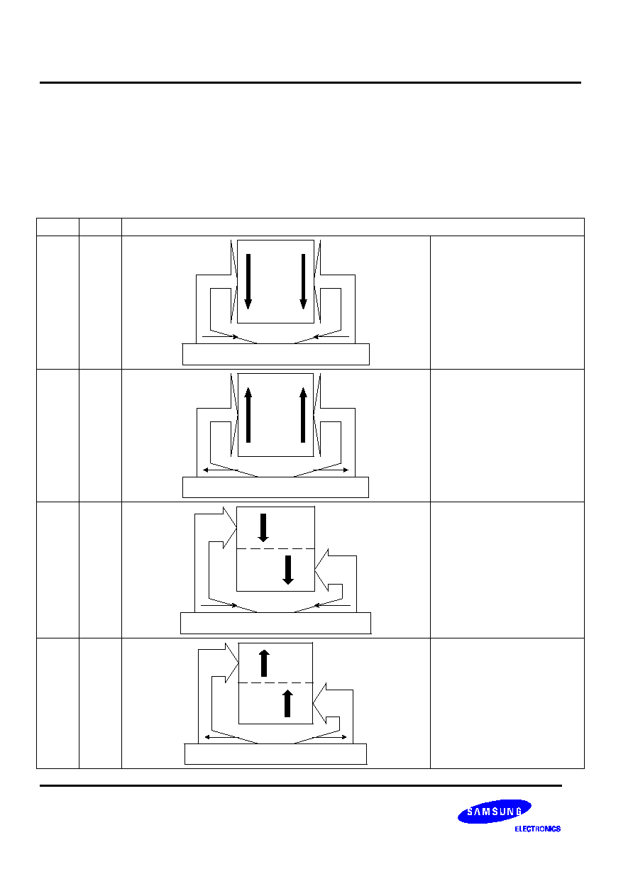
132-RGB X 176-DOT 1-CHIP DRIVER IC FOR 262,144-COLOR TFT-LCD DISPLAY
S6D0114
Preliminary
106
GATE DRIVER SCAN MODE SETTING
Gate scan mode of S6D0114 is set by SM and GS bit. GS bit determines the scan direction whether the gate driver
scans forward or reverse direction. SM bit determines the method of display division (Even/Odd or Upper/Lower
division drive). Using this function, various connections between S6D0114 and the liquid crystal panels can be
accomplished
Figure 76. Scan mode setting
SM
GS
Scan Mode
0
0
G1
G175
G2
G176
ODD
EVEN
TFT
Panel
G1
G175
G176
G2
S6D0110
G1
�
G2
�
G3
�
G4
�
����
�
G173
�
G174
�
G175
�
G176
0
1
S6D0110
G1
G175
G176
G2
G1
G175
G2
G176
ODD
EVEN
TFT
Panel
G174
�
G175
�
G176
G173
�
����
�
G4
�
G1
�
G2
�
G3
�
1
0
G1
G175
G2
G176
TFT
Panel
G1
G175
G176
G2
S6D0110
G1
�
G3
�
G5
�
����
�
G173
�
G175
G2
�
G4
�
G6
�
����
�
G174
�
G176
1
1
G1
G175
G2
G176
TFT
Panel
G1
G175
G176
G2
S6D0110
G176
�
G174
�
G172
�
����
�
G4
�
G2
G175
�
G173
�
G171
�
����
�
G3
�
G1
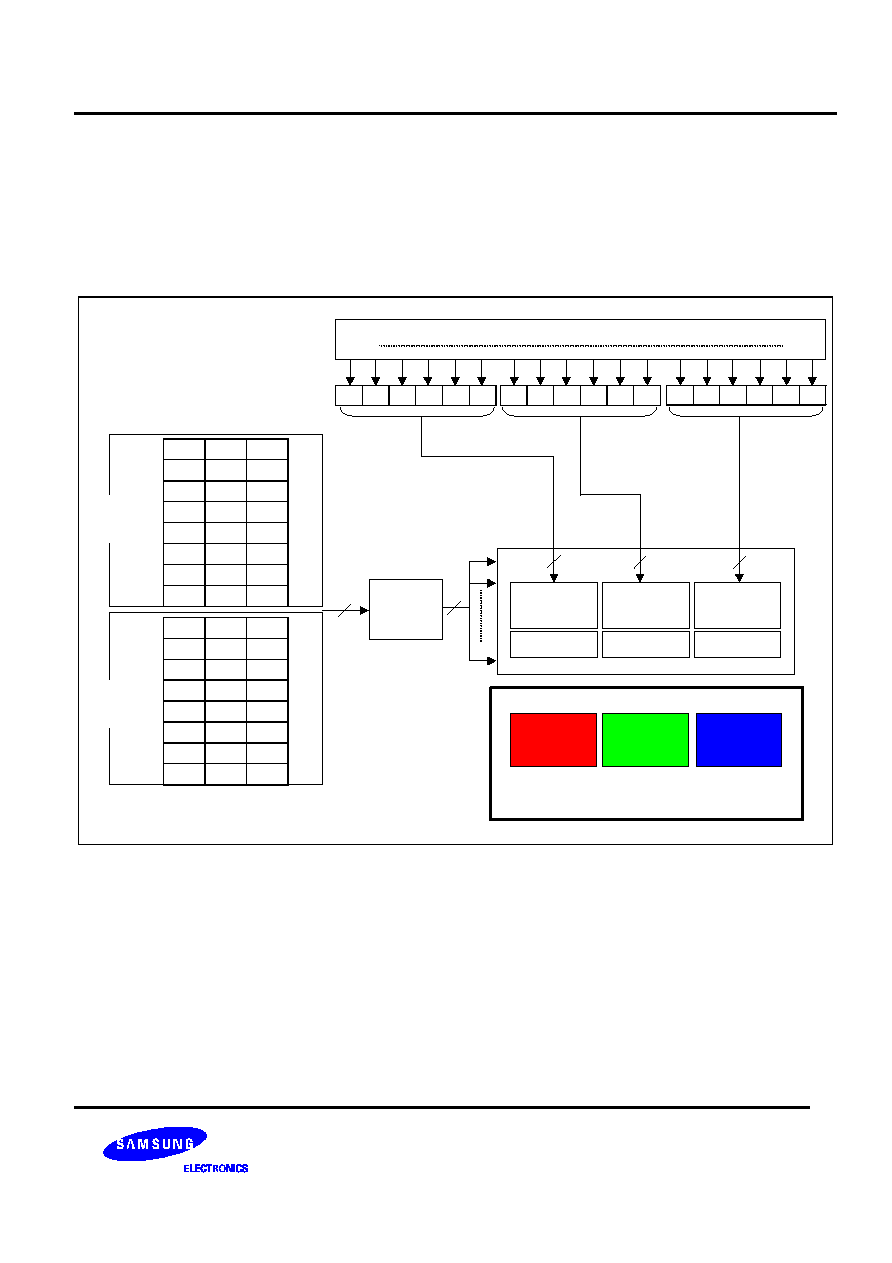
S6D0114 132-RGB X 176-DOT 1-CHIP DRIVER IC FOR 262,144-COLOR TFT-LCD DISPLAY
Preliminary
107
GAMMA ADJUSTMENT FUNCTION
The S6D0114 provides the gamma adjustment function to display 262,144 colors simultaneously. The gamma
adjustment executed by the gradient adjustment register and the micro-adjustment register that determines 8
grayscale levels. Furthermore, since the gradient adjustment register and the micro-adjustment register have the
positive polarities and negative polarities, adjust them to match LCD panel respectively.
G05
G04
G03
G02
G01
G00
Graphics RAM (GRAM)
MSB LSB
64-grayscale
control
<R>
64-grayscale
control
<G>
64-grayscale
control
<B>
LCD driver
LCD driver
LCD driver
R
G
B
LCD
Grayscale
amplifier
64
V0
V63
PKP02
PKP01
PKP00
PKP12
PKP11
PKP10
PKP22
PKP21
PKP20
PKP32
PKP31
PKP30
PKP42
PKP41
PKP40
PKP52
PKP51
PKP50
PRP02
PRP01
PRP00
PRP12
PRP11
PRP10
PKN02
PKN01
PKN00
PKN12
PKN11
PKN10
PKN22
PKN21
PKN20
PKN32
PKN31
PKN30
PKN42
PKN41
PKN40
PKN52
PKN51
PKN50
PRN02
PRN01
PRN00
PRN12
PRN11
PRN10
Positive
polarity
register
Negative
polarity
register
8
6
6
6
V1
R05
R04
R03
R02
R01
R00
B05
B04
B03
B02
B01
B00
Figure 77. Grayscale control

132-RGB X 176-DOT 1-CHIP DRIVER IC FOR 262,144-COLOR TFT-LCD DISPLAY
S6D0114
Preliminary
108
STRUCTURE OF GRAYSCALE AMPLIFIER
The structure of the grayscale amplifier is shown as below. Determine 8-level (VIN0-VIN7) by the gradient adjuster
and the micro adjustment register. Each level is split by the internal ladder resistance and level between V0 to V63
is generated.
Gradient adjustment
register
Micro adjustment register (6 X 3 bits)
PRP/N0 PRP/N1
PKP/N0 PKP/N1 PKP/N2 PKP/N3 PKP/N4 PKP/N5
Oscillation adjustment
register
VRP/VRN
8 to 1
selector
VDH
8 to 1
selector
8 to 1
selector
8 to 1
selector
8 to 1
selector
VGS
Ladder
resistance
Grayscale
amplifier
8 to 1
selector
3
3
3
3
3
3
3
3
5
VINP0/VINN0
VINP1/VINN1
VINP2/VINN2
VINP3/VINN3
VINP4/VINN4
VINP5/VINN5
VINP6/VINN6
VINP7/VINN7
V0
V1
V2
V3
V8
V9
V20
V21
V43
V44
V55
V56
V57
V62
V63
Figure 78. Structure of grayscale amplifier

S6D0114 132-RGB X 176-DOT 1-CHIP DRIVER IC FOR 262,144-COLOR TFT-LCD DISPLAY
Preliminary
109
8 to1
SEL
8 to1
SEL
8 to1
SEL
8 to1
SEL
8 to1
SEL
8 to1
SEL
KVP1
KVP2
KVP3
KVP4
KVP5
KVP6
KVP7
KVP8
KVP9
KVP10
KVP11
KVP12
KVP13
KVP14
KVP15
KVP16
KVP17
KVP18
KVP19
KVP20
KVP21
KVP22
KVP23
KVP24
KVP25
KVP26
KVP27
KVP28
KVP29
KVP30
KVP31
KVP32
KVP33
KVP34
KVP35
KVP36
KVP37
KVP38
KVP39
KVP40
KVP41
KVP42
KVP43
KVP44
KVP45
KVP46
KVP47
KVP48
v
v
v
v
v
v
VINP0
VINP1
VINP2
VINP3
VINP4
VINP5
VINP6
VINP7
KVP49
KVP0
PKP0[2:0]
PKP1[2:0]
PKP2[2:0]
PKP3[2:0]
PKP4[2:0]
PKP5[2:0]
PRP0[2:0]
PRP1[2:0]
VRP[2:0]
5R
4R
1R
1R
1R
1R
4R
5R
8R
VRP
0 to 31R
VRLP
0 to 28R
5R
16R
5R
VRHP
0 to 28R
RP0
RP1
RP2
RP3
RP4
RP5
RP6
RP7
RP8
RP9
RP10
RP11
RP12
RP13
RP14
RP15
RP16
RP17
RP18
RP19
RP20
RP21
RP22
RP23
RP24
RP25
RP26
RP27
RP28
RP29
RP30
RP31
RP32
RP33
RP34
RP35
RP36
RP37
RP38
RP39
RP40
RP41
RP42
RP43
RP44
RP45
RP46
RP47
8 to1
SEL
8 to1
SEL
8 to1
SEL
8 to1
SEL
8 to1
SEL
8 to1
SEL
KVN1
KVN2
KVN3
KVN4
KVN5
KVN6
KVN7
KVN8
KVN9
KVN10
KVN11
KVN12
KVN13
KVN14
KVN15
KVN16
KVN17
KVN18
KVN19
KVN20
KVN21
KVN22
KVN23
KVN24
KVN25
KVN26
KVN27
KVN28
KVN29
KVN30
KVN31
KVN32
KVN33
KVN34
KVN35
KVN36
KVN37
KVN38
KVN39
KVN40
KVN41
KVN42
KVN43
KVN44
KVN45
KVN46
KVN47
KVN48
v
v
v
v
v
v
VINN0
VINN1
VINN2
VINN3
VINN4
VINN5
VINN6
VINN7
KVN49
KVN0
PKN0[2:0]
PKN1[2:0]
PKN2[2:0]
PKN3[2:0]
PKN4[2:0]
PKN5[2:0]
PRN0[2:0]
PRN1[2:0]
VRN[2:0]
5R
4R
1R
1R
1R
1R
4R
5R
8R
VRN
0 to 31R
VRLN
0 to 28R
5R
16R
5R
VRHN
0 to 28R
RN0
RN1
RN2
RN3
RN4
RN5
RN6
RN7
RN8
RN9
RN10
RN11
RN12
RN13
RN14
RN15
RN16
RN17
RN18
RN19
RN20
RN21
RN22
RN23
RN24
RN25
RN26
RN27
RN28
RN29
RN30
RN31
RN32
RN33
RN34
RN35
RN36
RN37
RN38
RN39
RN40
RN41
RN42
RN43
RN44
RN45
RN46
RN47
EXVR
( )
VDH
Figure 79. Structure of Ladder / 8 to 1 selector

132-RGB X 176-DOT 1-CHIP DRIVER IC FOR 262,144-COLOR TFT-LCD DISPLAY
S6D0114
Preliminary
110
GAMMA ADJUSTMENT REGISTER
This block has the register to set up the grayscale voltage adjusting to the gamma specification of the LCD panel.
These registers can independently set up to positive/negative polarities and there are 3 types of register groups to
adjust gradient and oscillation on number of the grayscale, characteristics of the grayscale voltage. (average
<R><G><B> are common.) The following figure indicates the operation of each adjusting register.
Grayscale Number
Grayscale Voltage
a) Gradient adjustment
Grayscale Number
Grayscale Voltage
Grayscale Number
Grayscale Voltage
b) Oscillation adjustment
c) Micro-adjustment
Figure 80. The operation of adjusting register
a) Gradient adjustment resistor
The gradient adjustment resistors are used to adjust the gradient in the middle of the grayscale characteristics for
the voltage without changing the dynamic range. To accomplish the adjustment, it controls the variable resistor
(VRHP (N) / VRL (N)) of the ladder resistor for the grayscale voltage generator. Also, there is an independent
resistor on the positive/negative polarities in order for corresponding to asymmetry drive.
b) Oscillation adjustment resistor
The oscillation-adjusting resistor is to adjust oscillation of the grayscale voltage. To accomplish the adjustment, it
controls the variable resistor (VRP (N)) of the ladder resistor for the grayscale voltage generator located at lower
side of the ladder resistor. (Adjust upper side by input GVDD level.) Also, there is an independent resistor on the
positive/negative polarities as well as the gradient adjusting resistor.
c) Micro adjustment resistor
The micro adjustment resistor is to make subtle adjustment of the grayscale voltage level. To accomplish the
adjustment, it controls the each reference voltage level by the 8 to 1 selector towards the 8-leveled reference voltage
generated from the ladder resistor. Also, there is an independent resistor on the positive/negative polarities as well
as other adjusting resistors.

S6D0114 132-RGB X 176-DOT 1-CHIP DRIVER IC FOR 262,144-COLOR TFT-LCD DISPLAY
Preliminary
111
Table 36. Gamma correction registers
Register
Positive polarity
Negative polarity
Set-up contents
PRP0[2:0]
PRN0[2:0]
Variable resistor VRHP(N)
Gradient adjustment
PRP1[2:0]
PRN1[2:0]
Variable resistor VRLP(N)
Oscillation adjustment
VRP[4:0]
VRN[4:0]
Variable resistor VRP(N)
PKP0[2:0]
PKN0[2:0]
The voltage of grayscale number 1 is
selected by the 8 to 1 selector
PKP1[2:0]
PKN1[2:0]
The voltage of grayscale number 8 is
selected by the 8 to 1 selector
PKP3[2:0]
PKN3[2:0]
The voltage of grayscale number 20 is
selected by the 8 to 1 selector
PKP4[2:0]
PKN4[2:0]
The voltage of grayscale number 43 is
selected by the 8 to 1 selector
PKP5[2:0]
PKN5[2:0]
The voltage of grayscale number 55 is
selected by the 8 to 1 selector
Micro-adjustment
PKP6[2:0]
PKN6[2:0]
The voltage of grayscale number 62 is
selected by the 8 to 1 selector
132-RGB X 176-DOT 1-CHIP DRIVER IC FOR 262,144-COLOR TFT-LCD DISPLAY
S6D0114
Preliminary
112
LADDER RESISTOR/8 TO 1 SELECTOR
This block outputs the reference voltage of the grayscale voltage. There are two ladder resistors including the
variable resistor and the 8 to 1 selector selecting voltage generated by the ladder resistance voltage. The variable
and 8 to 1 resistors are controlled by the gamma resistor. Also, there are pins that connect to the external volume
resistor. And it allows to compensate the dispersion of length between one panel to another.
VARIABLE RESISTOR
There are 2 types of the variable resistors that is for the gradient adjustment (VRHP (N) / VRLP (N)) and for the
oscillation adjustment (VRP (N)). The resistance value is set by the gradient adjusting resistor and the oscillation
adjustiment resistor as below.
Table 37. Gradient Adjustment
Register value PRP(N) [2:0]
Resistance value PRP(N)
000
0R
001
4R
010
8R
011
12R
100
16R
101
20R
110
24R
111
28R
Table 38. Oscillation Adjustment
Register value VRP(N) [2:0]
Resistance value VRP(N)
00000
0R
00001
1R
00010
2R
.
.
.
.
.
.
11101
29R
11110
30R
11111
31R
S6D0114 132-RGB X 176-DOT 1-CHIP DRIVER IC FOR 262,144-COLOR TFT-LCD DISPLAY
Preliminary
113
THE 8 TO 1 SELECTOR
In the 8 to 1 selector, the voltage level must be selected given by the ladder resistance and the micro-adjusting
register. And output the voltage the six types of the reference voltage, the VIN1- to VIN6.
Following figure explains the relationship between the micro-adjusting register and the selecting voltage.
Table 39. Relationship between Micro-adjustment Register and Selected Voltage
Selected voltage
Register value
PKP(N) [2:0]
VINP(N)1
VINP(N)2
VINP(N)3
VINP(N)4
VINP(N)5
VINP(N)6
000
KVP(N)1
KVP(N)9
KVP(N)17
KVP(N)25
KVP(N)33
KVP(N)41
001
KVP(N)2
KVP(N)10
KVP(N)18
KVP(N)26
KVP(N)34
KVP(N)42
010
KVP(N)3
KVP(N)11
KVP(N)19
KVP(N)27
KVP(N)35
KVP(N)43
011
KVP(N)4
KVP(N)12
KVP(N)20
KVP(N)28
KVP(N)36
KVP(N)44
100
KVP(N)5
KVP(N)13
KVP(N)21
KVP(N)29
KVP(N)37
KVP(N)45
101
KVP(N)6
KVP(N)14
KVP(N)22
KVP(N)30
KVP(N)38
KVP(N)46
110
KVP(N)7
KVP(N)15
KVP(N)23
KVP(N)31
KVP(N)39
KVP(N)47
111
KVP(N)8
KVP(N)16
KVP(N)24
KVP(N)32
KVP(N)40
KVP(N)48

132-RGB X 176-DOT 1-CHIP DRIVER IC FOR 262,144-COLOR TFT-LCD DISPLAY
S6D0114
Preliminary
114
Table 40. Gamma Adjusting Voltage Formula (Positive polarity) 1
Pins
Formula
Micro-adjusting
register value
Reference
voltage
KVP0
GVDD
-
VINP0
KVP1
GVDD-
V*5R/SUMRP
PKP02-00 = "000"
KVP2
GVDD-
V*9R/SUMRP
PKP02-00 = "001"
KVP3
GVDD-
V*13R/SUMRP
PKP02-00 = "010"
KVP4
GVDD-
V*17R/SUMRP
PKP02-00 = "011"
KVP5
GVDD-
V*21R/SUMRP
PKP02-00 = "100"
KVP6
GVDD-
V*25R/SUMRP
PKP02-00 = "101"
KVP7
GVDD-
V*29R/SUMRP
PKP02-00 = "110"
KVP8
GVDD-
V*33R/SUMRP
PKP02-00 = "111"
VINP1
KVP9
GVDD-
V*(33R+VRHP)/SUMRP
PKP12-10 = "000"
KVP10
GVDD-
V*(34R+VRHP)/SUMRP
PKP12-10 = "001"
KVP11
GVDD-
V*(35R+VRHP)/SUMRP
PKP12-10 = "010"
KVP12
GVDD-
V*(36R+VRHP)/SUMRP
PKP12-10 = "011"
KVP13
GVDD-
V*(37R+VRHP)/SUMRP
PKP12-10 = "100"
KVP14
GVDD-
V*(38R+VRHP)/SUMRP
PKP12-10 = "101"
KVP15
GVDD-
V*(39R+VRHP)/SUMRP
PKP12-10 = "110"
KVP16
GVDD-
V*(40R+VRHP)/SUMRP
PKP12-10 = "111"
VINP2
KVP17
GVDD-
V*(45R+VRHP)/SUMRP
PKP22-20 = "000"
KVP18
GVDD-
V*(46R+VRHP)/SUMRP
PKP22-20 = "001"
KVP19
GVDD-
V*(47R+VRHP)/SUMRP
PKP22-20 = "010"
KVP20
GVDD-
V*(48R+VRHP)/SUMRP
PKP22-20 = "011"
KVP21
GVDD-
V*(49R+VRHP)/SUMRP
PKP22-20 = "100"
KVP22
GVDD-
V*(50R+VRHP)/SUMRP
PKP22-20 = "101"
KVP23
GVDD-
V*(51R+VRHP)/SUMRP
PKP22-20 = "110"
KVP24
GVDD-
V*(52R+VRHP)/SUMRP
PKP22-20 = "111"
VINP3
KVP25
GVDD-
V*(68R+VRHP)/SUMRP
PKP32-30 = "000"
KVP26
GVDD-
V*(69R+VRHP)/SUMRP
PKP32-30 = "001"
KVP27
GVDD-
V*(70R+VRHP)/SUMRP
PKP32-30 = "010"
KVP28
GVDD-
V*(71R+VRHP)/SUMRP
PKP32-30 = "011"
KVP29
GVDD-
V*(72R+VRHP)/SUMRP
PKP32-30 = "100"
KVP30
GVDD-
V*(73R+VRHP)/SUMRP
PKP32-30 = "101"
KVP31
GVDD-
V*(74R+VRHP)/SUMRP
PKP32-30 = "110"
KVP32
GVDD-
V*(75R+VRHP)/SUMRP
PKP32-30 = "111"
VINP4
KVP33
GVDD-
V*(80R+VRHP)/SUMRP
PKP42-40 = "000"
KVP34
GVDD-
V*(81R+VRHP)/SUMRP
PKP42-40 = "001"
KVP35
GVDD-
V*(82R+VRHP)/SUMRP
PKP42-40 = "010"
KVP36
GVDD-
V*(83R+VRHP)/SUMRP
PKP42-40 = "011"
KVP37
GVDD-
V*(84R+VRHP)/SUMRP
PKP42-40 = "100"
KVP38
GVDD-
V*(85R+VRHP)/SUMRP
PKP42-40 = "101"
KVP39
GVDD-
V*(86R+VRHP)/SUMRP
PKP42-40 = "110"
KVP40
GVDD-
V*(87R+VRHP)/SUMRP
PKP42-40 = "111"
VINP5
KVP41
GVDD-
V*(87R+VRHP+VRLP)/SUMRP
PKP52-50 = "000"
KVP42
GVDD-
V*(91R+VRHP+VRLP)/SUMRP
PKP52-50 = "001"
KVP43
GVDD-
V*(95R+VRHP+VRLP)/SUMRP
PKP52-50 = "010"
KVP44
GVDD-
V*(99R+VRHP+VRLP)/SUMRP
PKP52-50 = "011"
KVP45
GVDD-
V*(103R+VRHP+VRLP)/SUMRP
PKP52-50 = "100"
KVP46
GVDD-
V*(107R+VRHP+VRLP)/SUMRP
PKP52-50 = "101"
KVP47
GVDD-
V*(111R+VRHP+VRLP)/SUMRP
PKP52-50 = "110"
KVP48
GVDD-
V*(115R+VRHP+VRLP)/SUMRP
PKP52-50 = "111"
VINP6
KVP49
GVDD-
V*(120R+VRHP+VRLP)/SUMRP
-
VINP7
SUMRP: Total of the positive polarity ladder resistance = 128R + VRHP + VRLP + VRP
SUMRP: Total of the negative polarity ladder resistance = 128R + VRHN + VRLN + VRN
V: Potential difference between KV0 and KV49 = GVDD*SUMRP*SUMRN / [SUMRP*SUMRN+EXVR*(SUMRP+SUMRN)]
S6D0114 132-RGB X 176-DOT 1-CHIP DRIVER IC FOR 262,144-COLOR TFT-LCD DISPLAY
Preliminary
115
Table 41. Gamma Voltage Formula (Positive Polarity) 2
Grayscale voltage
Formula
Grayscale voltage
Formula
V0
VINP0
V32
V43+(V20-V43)*(11/23)
V1
VINP1
V33
V43+(V20-V43)*(10/23)
V2
V3+(V1-V3)*(8/24)
V34
V43+(V20-V43)*(9/23)
V3
V8+(V1-V8)*(450/800)
V35
V43+(V20-V43)*(8/23)
V4
V8+(V3-V8)*(16/24)
V36
V43+(V20-V43)*(7/23)
V5
V8+(V3-V8)*(12/24)
V37
V43+(V20-V43)*(6/23)
V6
V8+(V3-V8)*(8/24)
V38
V43+(V20-V43)*(5/23)
V7
V8+(V3-V8)*(4/24)
V39
V43+(V20-V43)*(4/23)
V8
VINP2
V40
V43+(V20-V43)*(3/23)
V9
V20+(V8-V20)*(22/24)
V41
V43+(V20-V43)*(2/23)
V10
V20+(V8-V20)*(20/24)
V42
V43+(V20-V43)*(1/23)
V11
V20+(V8-V20)*(18/24)
V43
VINP4
V12
V20+(V8-V20)*(16/24)
V44
V55+(V43-V55)*(22/24)
V13
V20+(V8-V20)*(14/24)
V45
V55+(V43-V55)*(20/24)
V14
V20+(V8-V20)*(12/24)
V46
V55+(V43-V55)*(18/24)
V15
V20+(V8-V20)*(10/24)
V47
V55+(V43-V55)*(16/24)
V16
V20+(V8-V20)*(8/24)
V48
V55+(V43-V55)*(14/24)
V17
V20+(V8-V20)*(6/24)
V49
V55+(V43-V55)*(12/24)
V18
V20+(V8-V20)*(4/24)
V50
V55+(V43-V55)*(10/24)
V19
V20+(V8-V20)*(2/24)
V51
V55+(V43-V55)*(8/24)
V20
VINP3
V52
V55+(V43-V55)*(6/24)
V21
V43+(V20-V43)*(22/23)
V53
V55+(V43-V55)*(4/24)
V22
V43+(V20-V43)*(21/23)
V54
V55+(V43-V55)*(2/24)
V23
V43+(V20-V43)*(20/23)
V55
VINP5
V24
V43+(V20-V43)*(19/23)
V56
V60+(V55-V60)*(20/24)
V25
V43+(V20-V43)*(18/23)
V57
V60+(V55-V60)*(16/24)
V26
V43+(V20-V43)*(17/23)
V58
V60+(V55-V60)*(12/24)
V27
V43+(V20-V43)*(16/23)
V59
V60+(V55-V60)*(8/24)
V28
V43+(V20-V43)*(15/23)
V60
V62+(V55-V62)*(350/800)
V29
V43+(V20-V43)*(14/23)
V61
V62+(V60-V62)*(16/24)
V30
V43+(V20-V43)*(13/23)
V62
VINP6
V31
V43+(V20-V43)*(12/23)
V63
VINP7
132-RGB X 176-DOT 1-CHIP DRIVER IC FOR 262,144-COLOR TFT-LCD DISPLAY
S6D0114
Preliminary
116
Table 42. Gamma Adjusting Voltage Formula (Negative polarity) 1
Pins
Formula
Micro-adjusting
register value
Reference
voltage
KVN0
GVDD
-
VINN0
KVN1
GVDD-
V*5R/SUMRN
PKN02-00 = "000"
KVN2
GVDD-
V*9R/SUMRN
PKN02-00 = "001"
KVN3
GVDD-
V*13R/SUMRN
PKN02-00 = "010"
KVN4
GVDD-
V*17R/SUMRN
PKN02-00 = "011"
KVN5
GVDD-
V*21R/SUMRN
PKN02-00 = "100"
KVN6
GVDD-
V*25R/SUMRN
PKN02-00 = "101"
KVN7
GVDD-
V*29R/SUMRN
PKN02-00 = "110"
KVN8
GVDD-
V*33R/SUMRN
PKN02-00 = "111"
VINN1
KVN9
GVDD-
V*(33R+VRHN)/SUMRN
PKN12-10 = "000"
KVN10
GVDD-
V*(34R+VRHN)/SUMRN
PKN12-10 = "001"
KVN11
GVDD-
V*(35R+VRHN)/SUMRN
PKN12-10 = "010"
KVN12
GVDD-
V*(36R+VRHN)/SUMRN
PKN12-10 = "011"
KVN13
GVDD-
V*(37R+VRHN)/SUMRN
PKN12-10 = "100"
KVN14
GVDD-
V*(38R+VRHN)/SUMRN
PKN12-10 = "101"
KVN15
GVDD-
V*(39R+VRHN)/SUMRN
PKN12-10 = "110"
KVN16
GVDD-
V*(40R+VRHN)/SUMRN
PKN12-10 = "111"
VINN2
KVN17
GVDD-
V*(45R+VRHN)/SUMRN
PKN22-20 = "000"
KVN18
GVDD-
V*(46R+VRHN)/SUMRN
PKN22-20 = "001"
KVN19
GVDD-
V*(47R+VRHN)/SUMRN
PKN22-20 = "010"
KVN20
GVDD-
V*(48R+VRHN)/SUMRN
PKN22-20 = "011"
KVN21
GVDD-
V*(49R+VRHN)/SUMRN
PKN22-20 = "100"
KVN22
GVDD-
V*(50R+VRHN)/SUMRN
PKN22-20 = "101"
KVN23
GVDD-
V*(51R+VRHN)/SUMRN
PKN22-20 = "110"
KVN24
GVDD-
V*(52R+VRHN)/SUMRN
PKN22-20 = "111"
VINN3
KVN25
GVDD-
V*(68R+VRHN)/SUMRN
PKN32-30 = "000"
KVN26
GVDD-
V*(69R+VRHN)/SUMRN
PKN32-30 = "001"
KVN27
GVDD-
V*(70R+VRHN)/SUMRN
PKN32-30 = "010"
KVN28
GVDD-
V*(71R+VRHN)/SUMRN
PKN32-30 = "011"
KVN29
GVDD-
V*(72R+VRHN)/SUMRN
PKN32-30 = "100"
KVN30
GVDD-
V*(73R+VRHN)/SUMRN
PKN32-30 = "101"
KVN31
GVDD-
V*(74R+VRHN)/SUMRN
PKN32-30 = "110"
KVN32
GVDD-
V*(75R+VRHN)/SUMRN
PKN32-30 = "111"
VINN4
KVN33
GVDD-
V*(80R+VRHN)/SUMRN
PKN42-40 = "000"
KVN34
GVDD-
V*(81R+VRHN)/SUMRN
PKN42-40 = "001"
KVN35
GVDD-
V*(82R+VRHN)/SUMRN
PKN42-40 = "010"
KVN36
GVDD-
V*(83R+VRHN)/SUMRN
PKN42-40 = "011"
KVN37
GVDD-
V*(84R+VRHN)/SUMRN
PKN42-40 = "100"
KVN38
GVDD-
V*(85R+VRHN)/SUMRN
PKN42-40 = "101"
KVN39
GVDD-
V*(86R+VRHN)/SUMRN
PKN42-40 = "110"
KVN40
GVDD-
V*(87R+VRHN)/SUMRN
PKN42-40 = "111"
VINN5
KVN41
GVDD-
V*(87R+VRHN+VRLN)/SUMRN
PKN52-50 = "000"
KVN42
GVDD-
V*(91R+VRHN+VRLN)/SUMRN
PKN52-50 = "001"
KVN43
GVDD-
V*(95R+VRHN+VRLN)/SUMRN
PKN52-50 = "010"
KVN44
GVDD-
V*(99R+VRHN+VRLN)/SUMRN
PKN52-50 = "011"
KVN45
GVDD-
V*(103R+VRHN+VRLN)/SUMRN
PKN52-50 = "100"
KVN46
GVDD-
V*(107R+VRHN+VRLN)/SUMRN
PKN52-50 = "101"
KVN47
GVDD-
V*(111R+VRHN+VRLN)/SUMRN
PKN52-50 = "110"
KVN48
GVDD-
V*(115R+VRHN+VRLN)/SUMRN
PKN52-50 = "111"
VINN6
KVN49
GVDD-
V*(120R+VRHN+VRLN)/SUMRN
-
VINN7
SUMRP: Total of the positive polarity ladder resistance = 128R + VRHP + VRLP + VRP
SUMRN: Total of the negative polarity ladder resistance = 128R + VRHN + VRLN + VRN
V: Potential difference between KV0 and KV49 = GVDD*SUMRP*SUMRN / [SUMRP*SUMRN+EXVR*(SUMRP+SUMRN)]

S6D0114 132-RGB X 176-DOT 1-CHIP DRIVER IC FOR 262,144-COLOR TFT-LCD DISPLAY
Preliminary
117
Table 43. Gamma Voltage Formula (Negative Polarity) 2
Grayscale voltage
Formula
Grayscale voltage
Formula
V0
VINN0
V32
V43+(V20-V43)*(11/23)
V1
VINN1
V33
V43+(V20-V43)*(10/23)
V2
V3+(V1-V3)*(8/24)
V34
V43+(V20-V43)*(9/23)
V3
V8+(V1-V8)*(450/800)
V35
V43+(V20-V43)*(8/23)
V4
V8+(V3-V8)*(16/24)
V36
V43+(V20-V43)*(7/23)
V5
V8+(V3-V8)*(12/24)
V37
V43+(V20-V43)*(6/23)
V6
V8+(V3-V8)*(8/24)
V38
V43+(V20-V43)*(5/23)
V7
V8+(V3-V8)*(4/24)
V39
V43+(V20-V43)*(4/23)
V8
VINN2
V40
V43+(V20-V43)*(3/23)
V9
V20+(V8-V20)*(22/24)
V41
V43+(V20-V43)*(2/23)
V10
V20+(V8-V20)*(20/24)
V42
V43+(V20-V43)*(1/23)
V11
V20+(V8-V20)*(18/24)
V43
VINN4
V12
V20+(V8-V20)*(16/24)
V44
V55+(V43-V55)*(22/24)
V13
V20+(V8-V20)*(14/24)
V45
V55+(V43-V55)*(20/24)
V14
V20+(V8-V20)*(12/24)
V46
V55+(V43-V55)*(18/24)
V15
V20+(V8-V20)*(10/24)
V47
V55+(V43-V55)*(16/24)
V16
V20+(V8-V20)*(8/24)
V48
V55+(V43-V55)*(14/24)
V17
V20+(V8-V20)*(6/24)
V49
V55+(V43-V55)*(12/24)
V18
V20+(V8-V20)*(4/24)
V50
V55+(V43-V55)*(10/24)
V19
V20+(V8-V20)*(2/24)
V51
V55+(V43-V55)*(8/24)
V20
VINN3
V52
V55+(V43-V55)*(6/24)
V21
V43+(V20-V43)*(22/23)
V53
V55+(V43-V55)*(4/24)
V22
V43+(V20-V43)*(21/23)
V54
V55+(V43-V55)*(2/24)
V23
V43+(V20-V43)*(20/23)
V55
VINN5
V24
V43+(V20-V43)*(19/23)
V56
V60+(V55-V60)*(20/24)
V25
V43+(V20-V43)*(18/23)
V57
V60+(V55-V60)*(16/24)
V26
V43+(V20-V43)*(17/23)
V58
V60+(V55-V60)*(12/24)
V27
V43+(V20-V43)*(16/23)
V59
V60+(V55-V60)*(8/24)
V28
V43+(V20-V43)*(15/23)
V60
V62+(V55-V62)*(350/800)
V29
V43+(V20-V43)*(14/23)
V61
V62+(V60-V62)*(16/24)
V30
V43+(V20-V43)*(13/23)
V62
VINN6
V31
V43+(V20-V43)*(12/23)
V63
VINN7
132-RGB X 176-DOT 1-CHIP DRIVER IC FOR 262,144-COLOR TFT-LCD DISPLAY
S6D0114
Preliminary
118
000000
111111
V63
V0
Output
Level
Negative Polarity
Positive Polarity
RAM data
(common charactersics to RGB)
Figure 81. Relationship between RAM data and output voltage
Positive polarity
Negative polarity
Sn
Vcom
Figure 82. Relationship between source output and Vcom
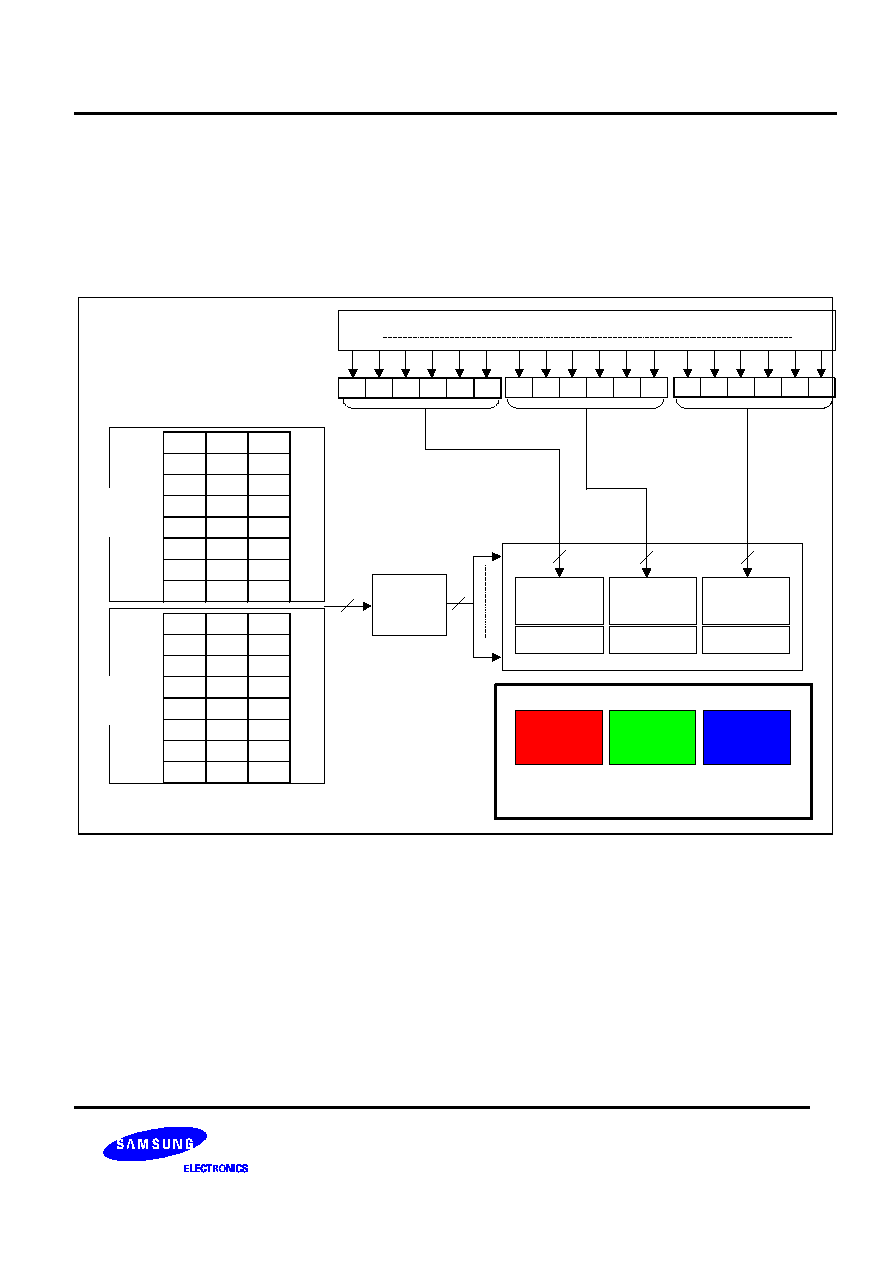
S6D0114 132-RGB X 176-DOT 1-CHIP DRIVER IC FOR 262,144-COLOR TFT-LCD DISPLAY
Preliminary
119
THE 8-COLOR DISPLAY MODE
The S6D0114 incorporates 8-color display mode. The grayscale levels to be used is V0 and V63 and all the other
levels (V1~V62) are halt. So that it attempts to lower power consumption.
During the 8-color mode, the Gamma micro adjustment register, PKP00-PKP52 and PKN00-PKN52 are invalid.
Since V1-V62 is stopped, the RGB data in the GRAM should be set to 000000 or 111111 before set the mode. The
level power supply (V1-V62) is in OFF condition during the 8-color mode in order to select V0/V63.
G05
G04
G03
G02
G01
G00
Graphics RAM (GRAM)
MSB LSB
R
G
B
LCD
Binary
amplifier
2
VDH
VGS
PKP02
PKP01
PKP00
PKP12
PKP11
PKP10
PKP22
PKP21
PKP20
PKP32
PKP31
PKP30
PKP42
PKP41
PKP40
PKP52
PKP51
PKP50
PRP02
PRP01
PRP00
PRP12
PRP11
PRP10
PKN02
PKN01
PKN00
PKN12
PKN11
PKN10
PKN22
PKN21
PKN20
PKN32
PKN31
PKN30
PKN42
PKN41
PKN40
PKN52
PKN51
PKN50
PRN02
PRN01
PRN00
PRN12
PRN11
PRN10
Positive
polarity
register
Negative
polarity
register
8
6
6
6
R05
R04
R03
R02
R01
R00
B05
B04
B03
B02
B01
B00
ON/OFF control
<R>
ON/OFF control
<G>
ON/OFF control
<B>
LCD driver
LCD driver
LCD driver
Figure 83. 8-color display control

132-RGB X 176-DOT 1-CHIP DRIVER IC FOR 262,144-COLOR TFT-LCD DISPLAY
S6D0114
Preliminary
120
OFF
GON="1"
DTE="1"
D1-0="10"
Wait (2 frame or higher)
ON
GON="1"
DTE="0"
D1-0="10"
OFF
GON="0"
DTE="0"
D1-0="00"
Wait (2 frame or higher)
RAM setup
CL="1"
Wait (40ms or higher)
ON
GON="0"
DTE="0"
D1-0="01"
Wait (2 frame or higher)
ON
GON="1"
DTE="0"
D1-0="01"
ON
GON="1"
DTE="0"
D1-0="11"
ON
GON="1"
DTE="1"
D1-0="11"
Display by 8-color mode
OFF
GON="1"
DTE="1"
D1-0="10"
Wait (2 frame or higher)
ON
GON="1"
DTE="0"
D1-0="10"
OFF
GON="0"
DTE="0"
D1-0="00"
Wait (2 frame or higher)
RAM setup
CL="0"
Wait (40ms or higher)
ON
GON="0"
DTE="0"
D1-0="01"
Wait (2 frame or higher)
ON
GON="1"
DTE="0"
D1-0="01"
ON
GON="1"
DTE="0"
D1-0="11"
ON
GON="1"
DTE="1"
D1-0="11"
Display
by 262,144-color mode
Wait (2 frame or higher)
Wait (2 frame or higher)
262,144-color => 8-color
8-color => 262,144 -color
Figure 84. Set up procedure for the 8-color mode

S6D0114 132-RGB X 176-DOT 1-CHIP DRIVER IC FOR 262,144-COLOR TFT-LCD DISPLAY
Preliminary
121
SYSTEM STRUCTURE EXAMPLE
Following diagram indicates the system structure, which composes the 132 (width) x 176 (length) dots TFT-LCD
panel.
T.B.D
Figure 85. System structure
132-RGB X 176-DOT 1-CHIP DRIVER IC FOR 262,144-COLOR TFT-LCD DISPLAY
S6D0114
Preliminary
122
Instruction set up flow
Display off
GON= 1
DTE= 1
D1-0= 10
Wait (more than 2 frames)
Display off
GON= 1
DTE= 0
D1-0= 10
Wait (more than 2 frames)
Display off
GON= 0
DTE= 0
D1-0= 00
Display OFF
Power off
SAP2-0= 000
AP2-0= 000
Continue to the display on flow
Power setting
Display on
GON= 0
DTE= 0
D1-0= 01
Wait (more than 2 frames)
Display on
GON= 1
DTE= 0
D1-0= 01
Display on
GON= 1
DTE= 0
D1-0= 11
Display on
GON= 1
DTE= 1
D1-0= 11
Display ON
Continue to the display on flow
<Display off>
<Display on>
EQ=0
Wait (more than 2 frames)
Figure 86. Instruction set up flow
S6D0114 132-RGB X 176-DOT 1-CHIP DRIVER IC FOR 262,144-COLOR TFT-LCD DISPLAY
Preliminary
123
<Standby>
<Sleep>
Display off flow
Standby set (STB= 1 )
Oscillation start
Wait 10ms
Standby cancel (STB= 0 )
Power setting
Display on flow
Display off flow
Sleep set (SLP= 1 )
Sleep cancel (SLP= 0 )
Power setting
Display on flow
Standby
set
Standby
cancel
Sleep
set
Sleep
Cancel
Figure 87. Instruction setup flow (continued)

132-RGB X 176-DOT 1-CHIP DRIVER IC FOR 262,144-COLOR TFT-LCD DISPLAY
S6D0114
Preliminary
124
OSCILLATION CIRCUIT
The S6D0114 can oscillate between the OSC1 and OSC2 pins using an internal R-C oscillator with an external
oscillation resistor. Note that in R-C oscillation, the oscillation frequency is changed according to the external
resistance value, wiring length, or operating power-supply voltage. If Rf is increased or power supply voltage is
decrease, the oscillation frequency decreases. For the relationship between Rf resistor value and oscillation
frequency, see the Electric Characteristics Notes section.
OSC1
OSC2
S6D0114
Clock
(200kHz)
Damping
resistance
(2k
)
1) External Clock Mode
2) External Resistance Oscillation Mode
OSC1
OSC2
S6D0114
Rf
NOTE: The Rf resistance must be located
near the OSC1/OSC2 pin on the chip
Figure 88. Oscillation Circuit
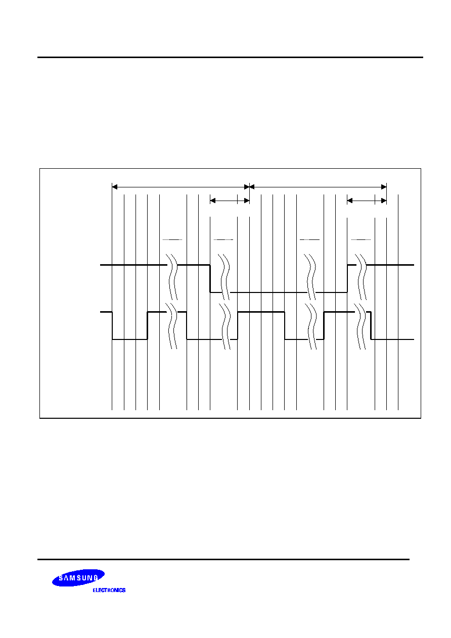
S6D0114 132-RGB X 176-DOT 1-CHIP DRIVER IC FOR 262,144-COLOR TFT-LCD DISPLAY
Preliminary
125
N-RASTER-ROW REVERSED AC DRIVE
The S6D0114 supports not only the LCD reversed AC drive in a one-frame unit but also the n-raster-row reversed
AC drive which alternates in an n-raster-row unit from one to 64 raster-rows. When a problem affecting display
quality occurs, the n-raster-row reversed AC drive can improve the quality.
Determine the number of the raster-rows n (NW bit set value +1) for alternating after confirmation of the display
quality with the actual LCD panel. However, if the number of AC raster-row is reduced, the LCD alternating
frequency becomes high. Because of this, the charge or discharge current is increased in the LCD cells.
1 2 3 4 175 176 184 1 2 3 4 175 176 184 1 2
1 frame
1 frame
Blank period
Blank period
Frame
A/C waveform drive
176 raster-row
N-raster-row
A/C waveform drive
176 raster-row
reverse 3 raster-row
EOR="1"
Figure 89. Example of an AC signal under n-raster-row reversed AC drive
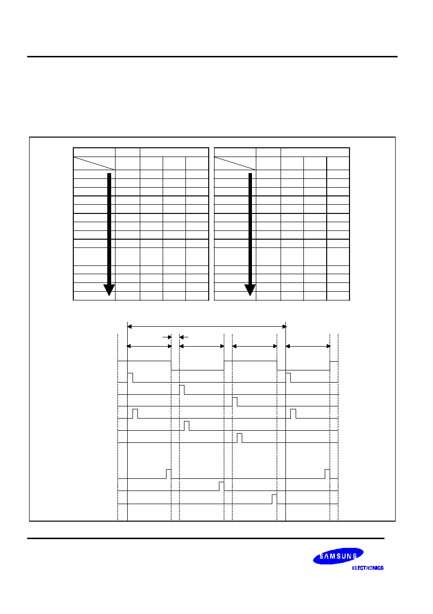
132-RGB X 176-DOT 1-CHIP DRIVER IC FOR 262,144-COLOR TFT-LCD DISPLAY
S6D0114
Preliminary
126
INTERLACE DRIVE
S6D0114 supports the interlace drive to protect from the flicker. It splits one frame into n fields and drives. Determine
the n fields (FLD bit stetting value) after confirming on the actual LCD display.
Following table indicates n fields: the gate selecting position when it is 1 or 3. and the diagram below indicates the
output waveform when the field interlace drive is active.
GS="0"
FLD1-0 setting value
01
11
Field
Gate
-
(1)
(2)
(3)
G1
G2
G3
G4
G5
G6
G7
G8
G9
G173
G174
G175
G176
GS="1"
FLD1-0 setting value
01
11
Field
Gate
-
(1)
(2)
(3)
G176
G175
G174
G173
G172
G171
G170
G169
G168
G4
G3
G2
G1
1 frame
Blank period
Field
(1)
Field
(2)
Field
(3)
Field
(1)
AC polarity
G1
G2
G3
G4
G5
G6
G3n+1
G3n+2
G3n+3
Figure 90. Interlace drive and output waveform
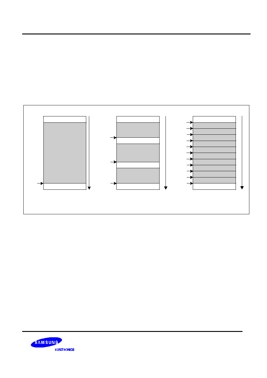
S6D0114 132-RGB X 176-DOT 1-CHIP DRIVER IC FOR 262,144-COLOR TFT-LCD DISPLAY
Preliminary
127
A/C TIMING
Following diagram indicates the A/C timing on the each A/C drive method. After every 1 drawing, the A/C timing is
occurred on the reversed frame AC drive. After the A/C timing, the blank (all gate output: Vgoff level) period
described below is inserted. When it is on the interlace drive, blank period is inserted every A/C timing. When the
reversed n-raster-row is driving, a blank period is inserted after all screens are drawn. Front and Back porch can be
adjusted using FP3-0 and BP3-0 bits (R08h). In interlace drive mode, Blank period can be adjusted using BLP13-0
and BLP23-0 bit (R09h).
Blank period = Back porch
+ Blank period 1
+ Blank period 2
+ Front porch
Frame 1
Frame reverse AC drive
1 frame period
Field 1
A/C
A/C
A/C
Blank period = Back porch
+ Front Porch
3 field interlace drive
n-raster-row reversed AC drive
Front porch
Back porch
A/C
timing
1 frame period
Front porch
Field 2
Field 3
Blank period 2 (BLP2)
Blank period 1 (BLP1)
Back porch
A/C
1 frame period
Front porch
Back porch
A/C
A/C
A/C
A/C
A/C
A/C
A/C
A/C
A/C
A/C
n-raster-row
Blank period = Back porch
+ Front Porch
n-raster-row
n-raster-row
n-raster-row
n-raster-row
n-raster-row
n-raster-row
n-raster-row
n-raster-row
n-raster-row
Figure 91. A/C timing

132-RGB X 176-DOT 1-CHIP DRIVER IC FOR 262,144-COLOR TFT-LCD DISPLAY
S6D0114
Preliminary
128
FRAME FREQUENCY ADJUSTING FUNCTION
The S6D0114 has an on-chip frame-frequency adjustment function. The frame frequency can be adjusted by the
instruction setting (DIV, RTN) during the LCD driver as the oscillation frequency is always same.
If the oscillation frequency is set to high, animation or a static image can be displayed in suitable ways by changing
the frame frequency. When a static image is displayed, the frame frequency can be set low and the low-power
consumption mode can be entered. When high-speed screen switching for an animated display, etc. is required, the
frame frequency can be set high.
RELATIONSHIP BETWEEN LCD DRIVE DUTY AND FRAME FREQUENCY
The relationships between the LCD drive duty and the frame frequency is calculated by the following expression.
The frame frequency can be adjusted in the 1H period adjusting bit (RTN) and in the operation clock division bit
(DIV) by the instruction.
Frame Frequency =
f
OSC
Clock cycles per raster-row x division ratio x (Line+B)
[Hz]
f
OSC
: R-C oscillation frequency
Line: Number of raster-rows (NL bit)
Clock cycles per raster-row: RTN bit
Division ratio: DIV bit
B: Blank period(Back porch + Front Porch)
Figure 92. Formula for the frame frequency
Example calculation
Driver raster-row: 176
1H period: 16 clock (RTN3 to 0 = 0000)
Operation clock division ratio: 1division
B: Blank period (BP + FP): 8
fosc = 60Hz x (0+16) clock x 1 division x (176+B) lines = 177 [kHz]
In this case, the RC oscillation frequency becomes 177 kHz. The external resistance value of the RC oscillator must
be adjusted to be 177 kHz.
Note: When FLD1-0="11"(interlace drive), B = BP + FP + BLP1 + BLP2
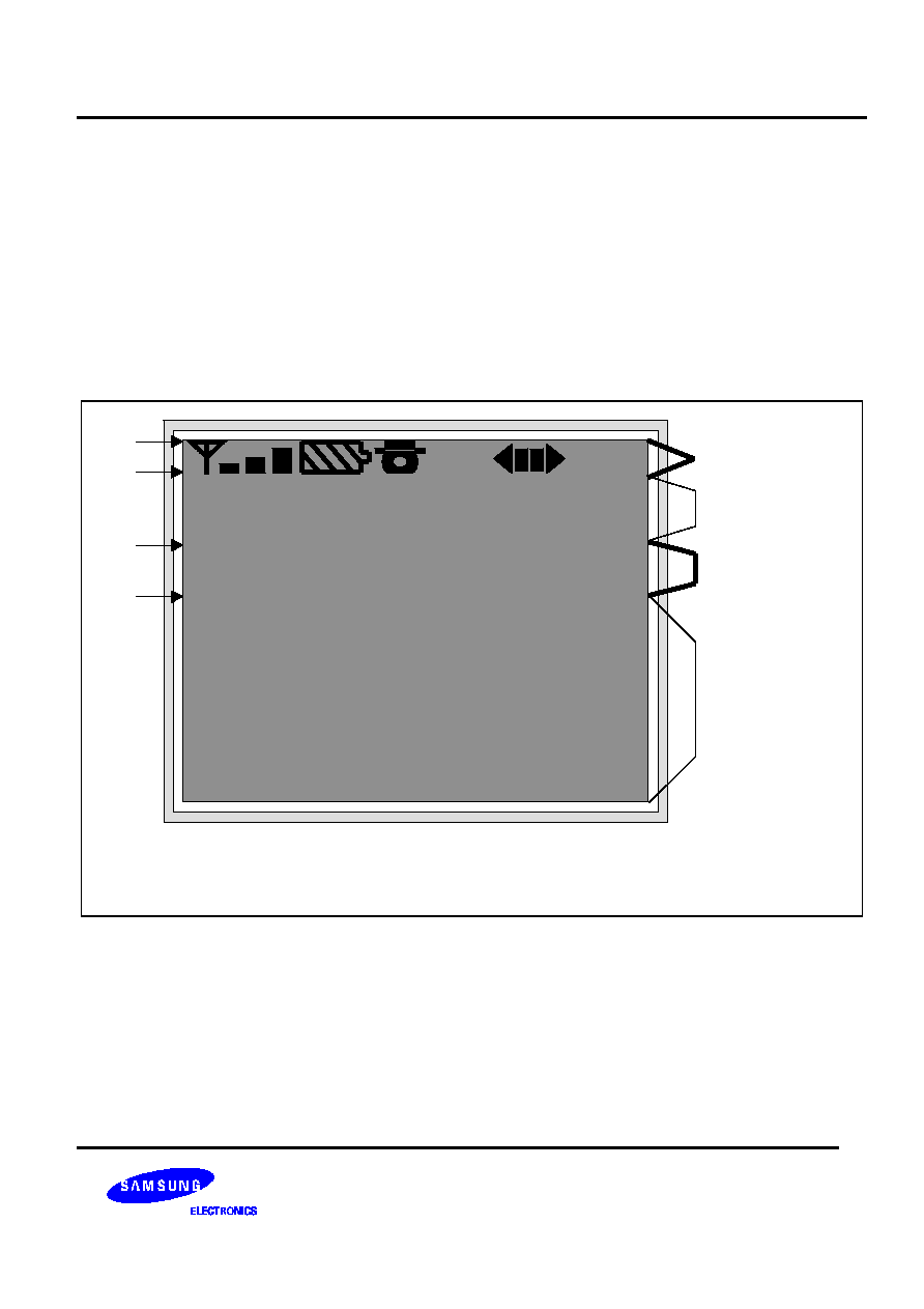
S6D0114 132-RGB X 176-DOT 1-CHIP DRIVER IC FOR 262,144-COLOR TFT-LCD DISPLAY
Preliminary
129
SCREEN-DIVISION DRIVING FUNCTION
The S6D0114 can select and drive two screens at any position with the screen-driving position registers (R14 and
R15). Any two screens required for display are selectively driven and reducing LCD-driving voltage and power
consumption.
For the 1
st
division screen, start line (SS17 to 10) and end line (SE17 to 10) are specified by the 1
st
screen-driving
position register (R14). For the 2
nd
division screen, start line (SS27 to 20) and end line (SE27 to 20) are specified by
the 2
nd
screen-driving position register (R15). The 2
nd
screen control is effective when the SPT bit is 1. The total
count of selection-driving lines for the 1
st
and 2
nd
screens must correspond to the LCD-driving duty set value.
Rm
*
OCT 14th 10:18am
G1
G7
G26
G42
1st screen:
7-raster-row driving
Non-display area
2nd screen:
17 raster-row driving
Non-display area
�
Driving raster-row: NL4-0 = 10101 (176 lines)
�
1st screen setting: SS17-10 = 00H, SE17-10 = 06H
�
2nd screen setting: SS27-20 = 19H, SE27-20 = 29H, SPT = 1
Figure 93. Driving on 2 screen
132-RGB X 176-DOT 1-CHIP DRIVER IC FOR 262,144-COLOR TFT-LCD DISPLAY
S6D0114
Preliminary
130
RESTRICTION ON THE 1
ST
/2
ND
SCREEN DRIVING POSITION REGISTER SETTINGS
The following restrictions must be satisfied when setting the start line (SS17 to 10) and end line (SE17 to 10) of the
1
st
screen driving position register (R42H) and the start line (SS27 to 20) and end line (SE27 to 20) of the 2
nd
screen
driving position register (R43H) for the S6D0114. Note that incorrect display may occur if the restrictions are not
satisfied.
Table 44. Restrictions on the 1
st
/2
nd
Screen Driving Position Register Setting
1
st
Screen Driving (SPT=0)
Register setting
Display operation
(SE17 to 10) � (SS17 to 10) = NL
Full screen display
Normally displays (SE17 to 10) to (SS17 to 10)
(SE17 to 10) � (SS17 to 10) < NL
Partial display
Normally displays (SE17 to 10) to (SS17 to 10)
White display for all other times (RAM data is not related
at all)
(SE17 to 10) � (SS17 to 10) > NL
Setting disabled
NOTE 1: SS17 to 10
SE17 to 10
AFh
NOTE 2: Setting SE27 to 20 and SS27 to 20 are invalid
2
nd
Screen Driving (SPT=1)
Register setting
Display operation
((SE17 to 10) � (SS17 to 10))
+ ((SE27 to 20) � (SS27-20)) = NL
Full screen display
Normally displays (SE27 to 10) to (SS17 to 10)
((SE17 to 10) � (SS17 to 10))
+ ((SE27 to 20) � (SS27-20)) < NL
Partial display
Normally displays (SE27 to 10) to (SS17 to 10)
White display for all other times (RAM data is not related
at all)
((SE17 to 10) � (SS17 to 10))
+ ((SE27 to 20) � (SS27-20)) > NL
Setting disabled
NOTE 1: SS17 to 10
SE17 to 10 < SS27 to 20
SE27 to 20
AFh
NOTE 2: (SE27 to 20) � (SS17 to 10)
NL
The driver output can't be set for non-display area during the partial display. Determine based on specification of the
panels.
Source output in non-display area
PT1
PT0
Positive polarity
Negative polarity
Gate output in
Non-display area
0
0
V63
V0
Normal drive
0
1
V63
V0
Vgoff
1
0
VSS
VSS
Vgoff
1
1
Hi-Z
Hi-Z
Vgoff
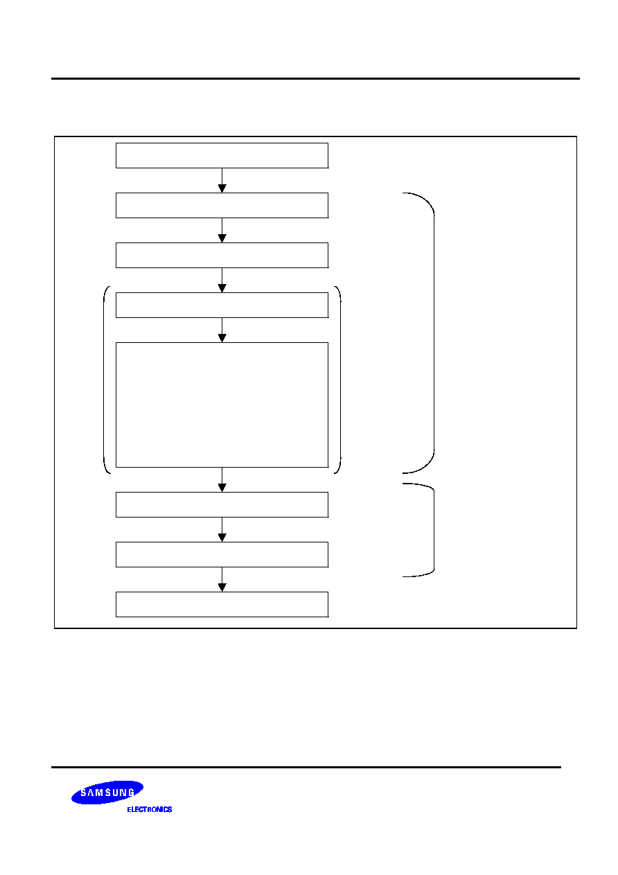
S6D0114 132-RGB X 176-DOT 1-CHIP DRIVER IC FOR 262,144-COLOR TFT-LCD DISPLAY
Preliminary
131
Refer to the following flow to set up the partial display.
Full screen display
PT1-0 = 00
Set SS/SE bits
Wait (more than 2 frames)
PT1-0 = 01
or
PT1-0 = 10
or
PT1-0 = 11
Partial display on
Set SS/SE bits
Full screen display
Set as need
Setting flow for
full screen driver
Split screen drive
set up flow
Figure 94. Partial display set up flow

132-RGB X 176-DOT 1-CHIP DRIVER IC FOR 262,144-COLOR TFT-LCD DISPLAY
S6D0114
Preliminary
132
APPLICATION CIRCUIT
The following figure indicates a schematic diagram of application circuit for S6D0114.
T.B.D
Figure 95. Application Circuit
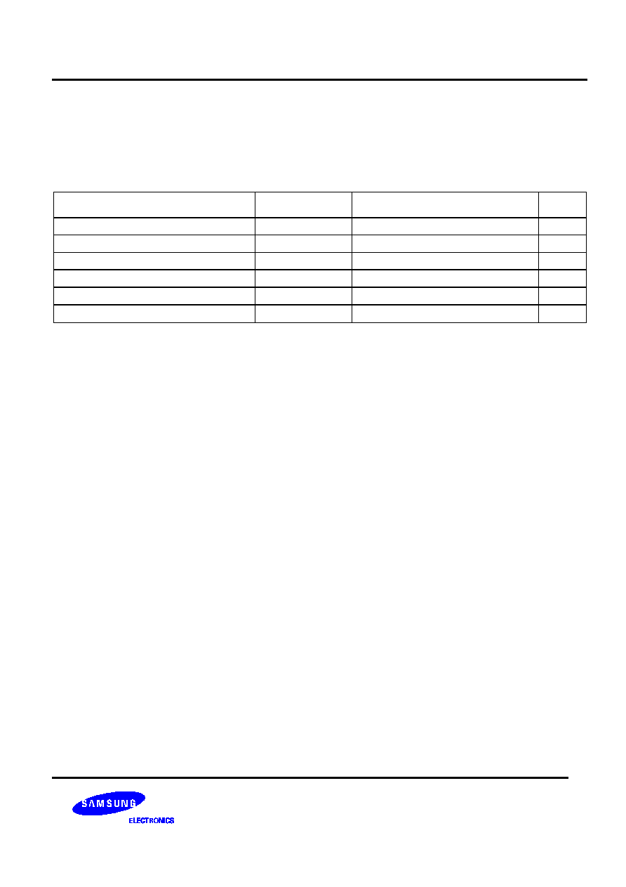
S6D0114 132-RGB X 176-DOT 1-CHIP DRIVER IC FOR 262,144-COLOR TFT-LCD DISPLAY
Preliminary
133
SPECIFICATIONS
ABSOLUTE MAXIMUM RATINGS
Table 45. Absolute Maximum Rating
(VSS = 0V)
Item
Symbol
Rating
Unit
Supply voltage
VDD
- 0.3 ~ + 5.0
V
Supply voltage for step-up circuit
Vci
- 0.3 ~ + 5.0
V
LCD Supply Voltage range
|VGH � VGL|
30
V
Input Voltage range
Vin
- 0.3 to VDD +0.5
V
Operating temperature
T
opr
-40 ~ +85
�
C
Storage temperature
T
stg
-55 ~ +110
�
C
Notes:
1. Absolute maximum rating is the limit value beyond which the IC may be broken. They do not assure operations.
2. Operating temperature is the range of device-operating temperature. They do not guarantee chip performance.
3. Absolute maximum rating is guaranteed when our company's package used.
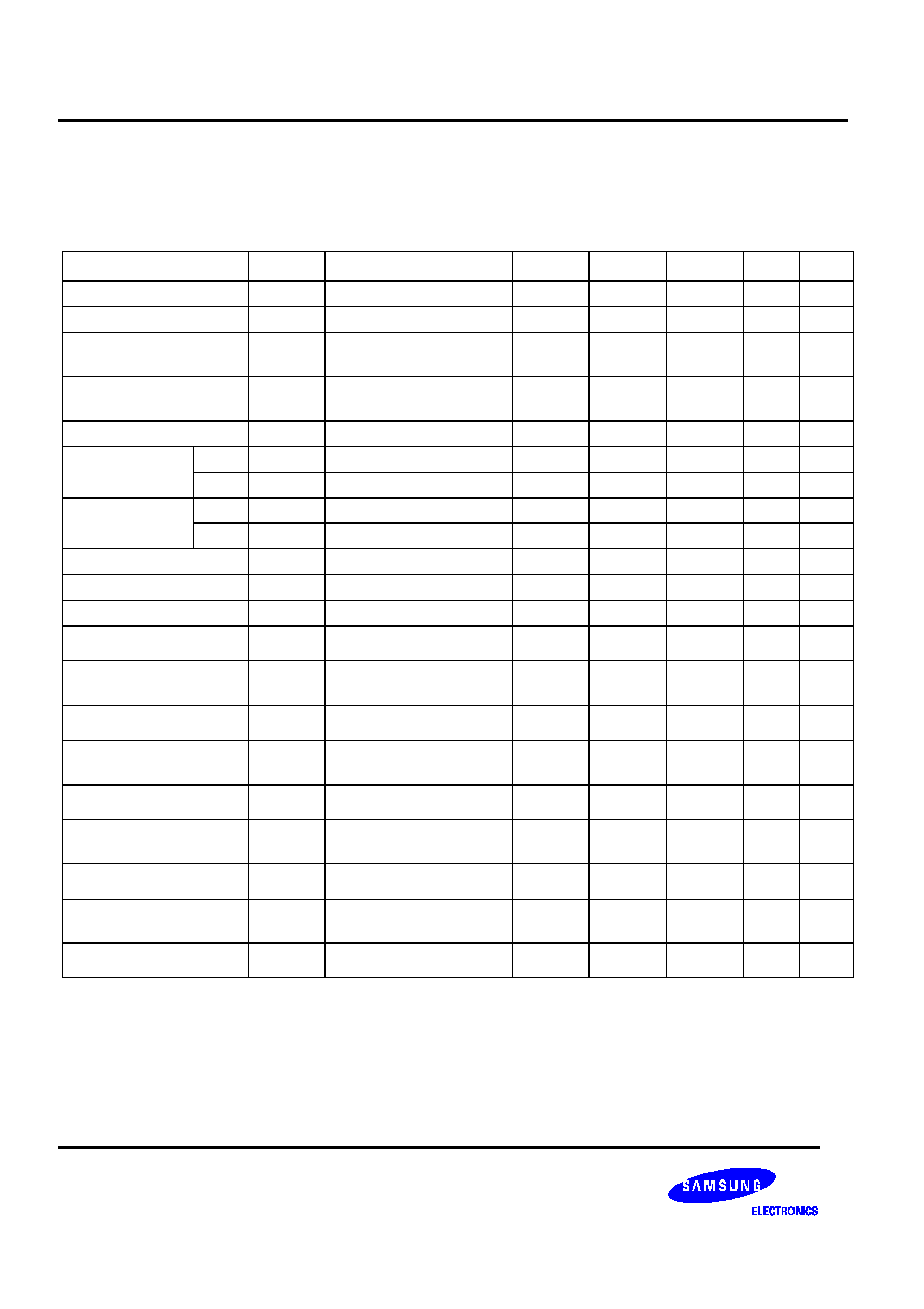
132-RGB X 176-DOT 1-CHIP DRIVER IC FOR 262,144-COLOR TFT-LCD DISPLAY
S6D0114
Preliminary
134
DC CHARACTERISTICS
Table 46. DC Characteristics
((VDD = 1.8V or VDD3 = 3.3V), GVDD = 4.5V, AVDD = 5.0V, VSS = 0V)
Characteristic
Symbol
CONDITION
MIN
TYP
MAX
Unit
Note
Operating voltage(1)
VDD
1.8
-
2.5
V
*1
Operating voltage(2)
VDD3
2.3
-
3.3
V
*1
Driver positive power
supply
VGH
+7
-
20.0
V
Driver negative power
supply
VGL
-7
-
-15.0
V
Gate off power supply
Vgoff
-5
-
-15
V
*2
High
V
IH
0.7XVDD
-
VDD
V
*2
Logic
Input Voltage
Low
V
IL
0
-
0.3XVDD
V
*3
High
V
OH
I
OH
= -2.0mA
VDD-0.5
VDD
V
*3
Logic
Output Voltage
Low
V
OL
I
OL
= 2.0mA
0.0
-
0.5
V
Input leakage current
I
IL
VIN = VSS or VDD
-1.0
-
1.0
�
A
*2
Output leakage current
I
OL
VIN = VSS or VDD
-3.0
-
3.0
�
A
*3
Operating frequency
fosc
-
KHz
*5
1
st
step-up input voltage
Vci1
-
2.5
-
3.3
V
1
st
step-up output
efficiency
AVDD
%
2
nd
step-up input voltage
Vci2
4.5
5.5
V
2
nd
step-up output
efficiency
VGH
%
3
rd
step-up input voltage
Vci3
20
V
3
rd
step-up output
efficiency
VGL
94
99
%
4
th
step-up input voltage
Vci4
2.5
3.3
V
4
th
step-up output
efficiency
VCL
%
-
-
TBD
�
A
*6
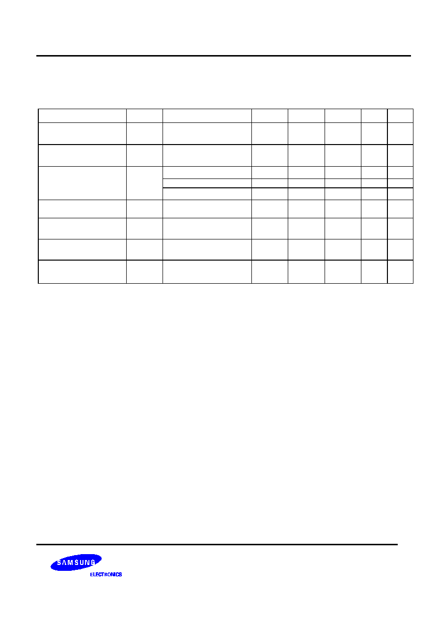
S6D0114 132-RGB X 176-DOT 1-CHIP DRIVER IC FOR 262,144-COLOR TFT-LCD DISPLAY
Preliminary
135
Table 47. DC Characteristics for LCD driver outputs
((VDD = 1.8V or VDD3 = 3.3V), GVDD = 4.5V, AVDD = 5.0V, VSS = 0V)
Characteristic
Symbol
CONDITION
MIN
TYP
MAX
Unit
Note
High-level output current
(Gradation output)
IOH1
Vx = 4.5V, Vout = 3.5V
-
-
-0.05
mA
*4
Low-level output current
(Gradation output)
IOL1
Vx = 0.1V, Vout = 1.1V
0.05
-
-
mA
*4
4.2V
V
X
-
�
20
�
30
mV
0.8V < V
X
< 4.2V
-
�
10
�
20
mV
Output voltage deviation
(Mean value)
Vo
V
X
0.8V
-
�
20
�
30
mV
Output voltage range
V
O
-
GVDD+0.
1
-
GVDD-
0.1
V
High-level output current
(Binary output)
I
OH2
V
X
= 5V, V
OUT
= 4V,
-
-
-0.1
mA
Low-level output current
(Binary output)
I
OL2
V
X
= 0.0V, V
OUT
= 1.0V
0.1
-
-
mA
Gate Driver On
Resistance
R
ONG
Ta = 25
�
C
VGH � VGL = 26V
I load = +/- 100 uA
-
-
1.0
k
*4
Notes :
1. VSS = 0V.
2. CSB, RS, DB0 to DB17, E, RW, RESETB.
3. DB0 to DB17, CL.
4. Resistance value when �0.1[mA] is applied during the ON status of the output pin Sn or Gn.
RON[k �] = �V [V] / 0.1 [mA] (�V : Voltage change when �0.1[mA] is applied in the ON status)
5. fosc = fCL x CL division.
f
FRAME
= fCL / 2 / Display duty ratio.
6. Dynamic current condition : VDD=VCI=2.7V, VDDI=1.8V, x3, 1/5 bias, fosc = 115.2 kHz, f
FRAME
= 180 Hz,
V3 � MV3 = 19.6V, V2 = 7.84V
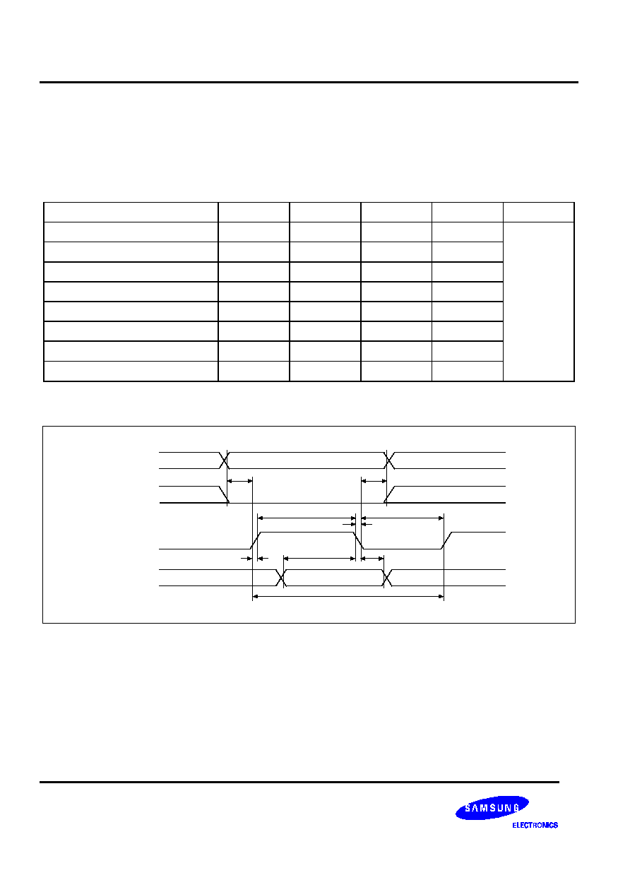
132-RGB X 176-DOT 1-CHIP DRIVER IC FOR 262,144-COLOR TFT-LCD DISPLAY
S6D0114
Preliminary
136
AC CHARACTERISTICS
Parallel Write Interface (68 Mode, HWM =1)
Table 48. Parallel Write Interface Characteristic (68 Mode, HWM =1)
(VDD = 1.8V to 2.7V, T
A
= -30 to +85
o
C)
Characteristic
Symbol
Min.
Typ.
Max.
Unit
E_RD cycle time
t
C
62
-
-
Pulse rise / fall time
t
R
,t
F
-
-
3
E_RD pulse width high
t
WH
30
-
-
E_RD pulse width low
t
WL
30
-
-
RS and CSB setup time
t
SU1
10
-
-
RS and CSB hold time
t
H1
10
-
-
DB setup time
t
SU2
20
-
-
DB hold time
t
H2
10
-
-
ns
R S , C S B
R W _ W R B
E _ R D B
D B 1 7 ~ 0
V L D
t
S U 1
t
H 1
t
W H
t
W L
t
R
t
S U 2
t
C
t
H 2
t
F
V a lid D a ta
Figure 96. Burst Write Timing Diagram (68-series)
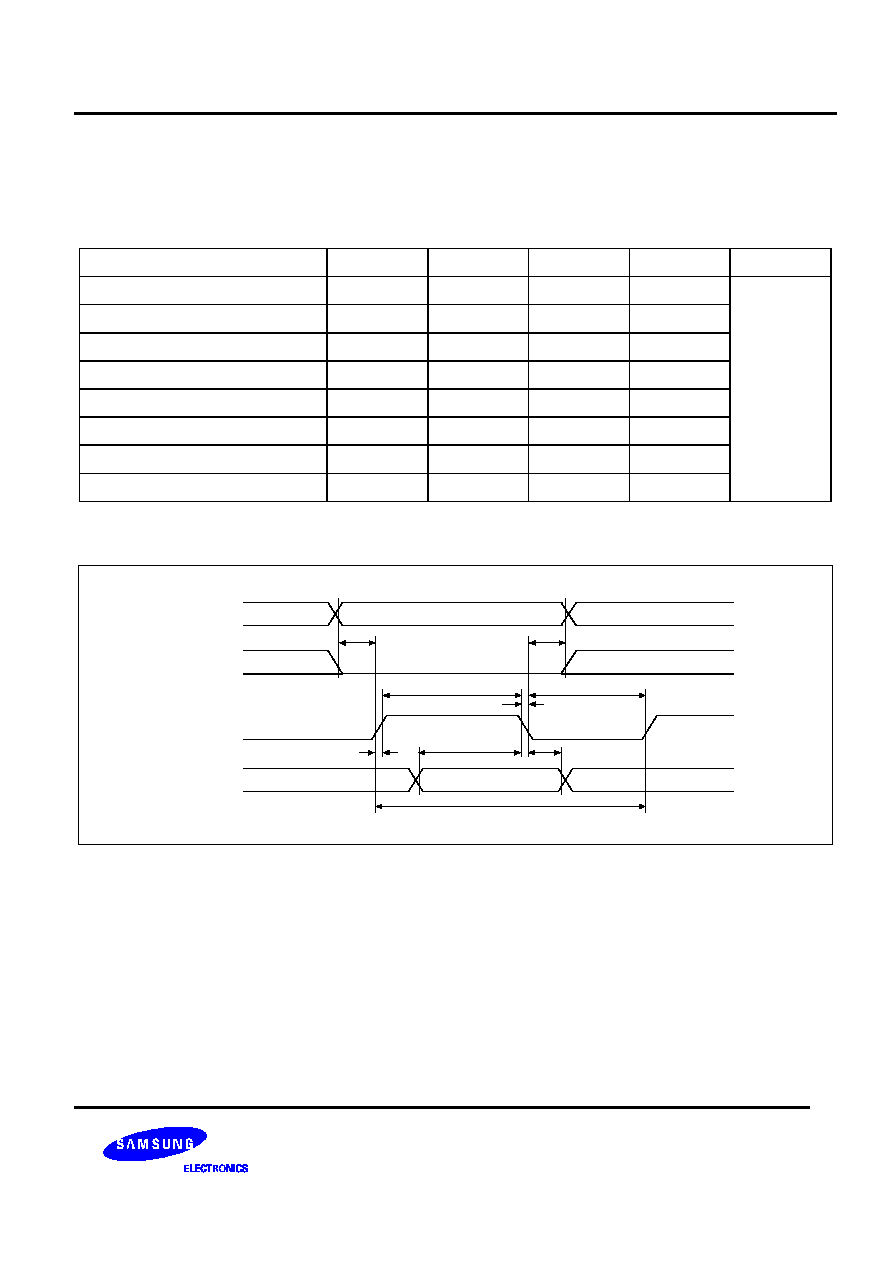
S6D0114 132-RGB X 176-DOT 1-CHIP DRIVER IC FOR 262,144-COLOR TFT-LCD DISPLAY
Preliminary
137
Parallel Write Interface (68 Mode, HWM =0)
Table 49. Parallel Write Interface Characteristic (68 Mode, HWM =0)
(V
DD
= 1.8V to 2.7V, T
A
= -30 to +85
o
C)
Characteristic
Symbol
Min.
Typ.
Max.
Unit
E_RD cycle time
t
C
250
-
-
Pulse rise / fall time
t
R
,t
F
-
-
10
E_RD pulse width high
t
WH
100
-
-
E_RD pulse width low
t
WL
100
-
-
RS and CSB setup time
t
SU1
10
-
-
RS and CSB hold time
t
H1
10
-
-
DB setup time
t
SU2
20
-
-
DB hold time
t
H2
10
-
-
ns
R S , C S B
R W _ W R B
E _ R D B
D B 1 7 ~ 0
V L D
t
S U 1
t
H 1
t
W H
t
W L
t
R
t
S U 2
t
C
t
H 2
t
F
V a lid D a ta
Figure 97. Single Write Timing Diagram (68-series)
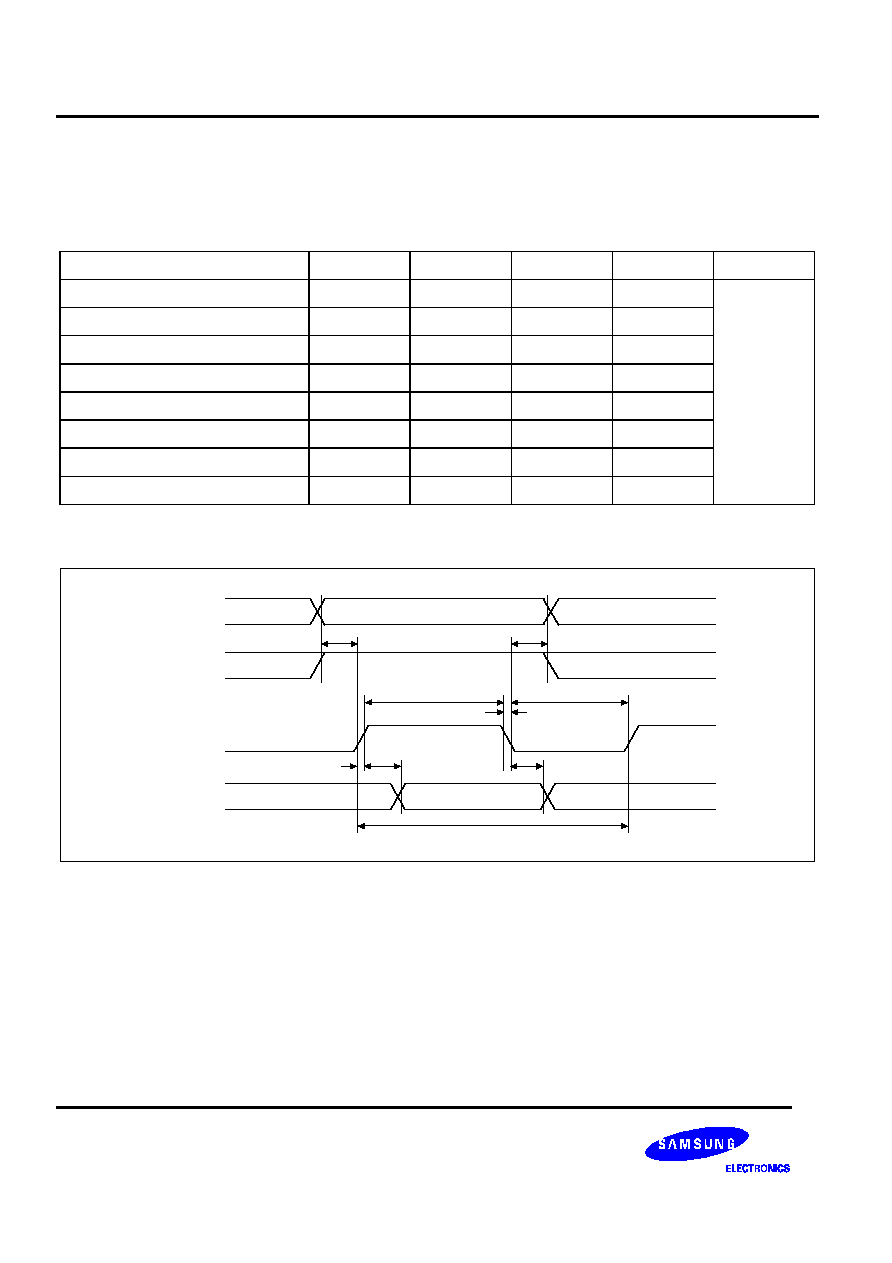
132-RGB X 176-DOT 1-CHIP DRIVER IC FOR 262,144-COLOR TFT-LCD DISPLAY
S6D0114
Preliminary
138
Parallel Read Interface (68 Mode)
Table 50. Parallel Read Interface Characteristic (68 Mode)
(V
DD
= 1.8V to 2.7V, T
A
= -30 to +85
o
C)
Characteristic
Symbol
Min.
Typ.
Max.
Unit
E_RD cycle time
t
C
450
-
-
Pulse rise / fall time
t
R
,t
F
-
-
10
E_RD pulse width high
t
WH
200
-
-
E_RD pulse width low
t
WL
200
-
-
RS and CSB setup time
t
SU
10
-
-
RS and CSB hold time
t
H
10
-
-
DB output delay time
t
D
20
-
-
DB output hold time
T
dh
10
-
-
ns
RS,CSB
RW_WRB
E_RDB
DB17~0
t
SU
t
H
t
W H
t
W L
t
R
t
C
t
D
t
DH
Valid Data
t
F
Figure 98. Read Timing Diagram (68-series)
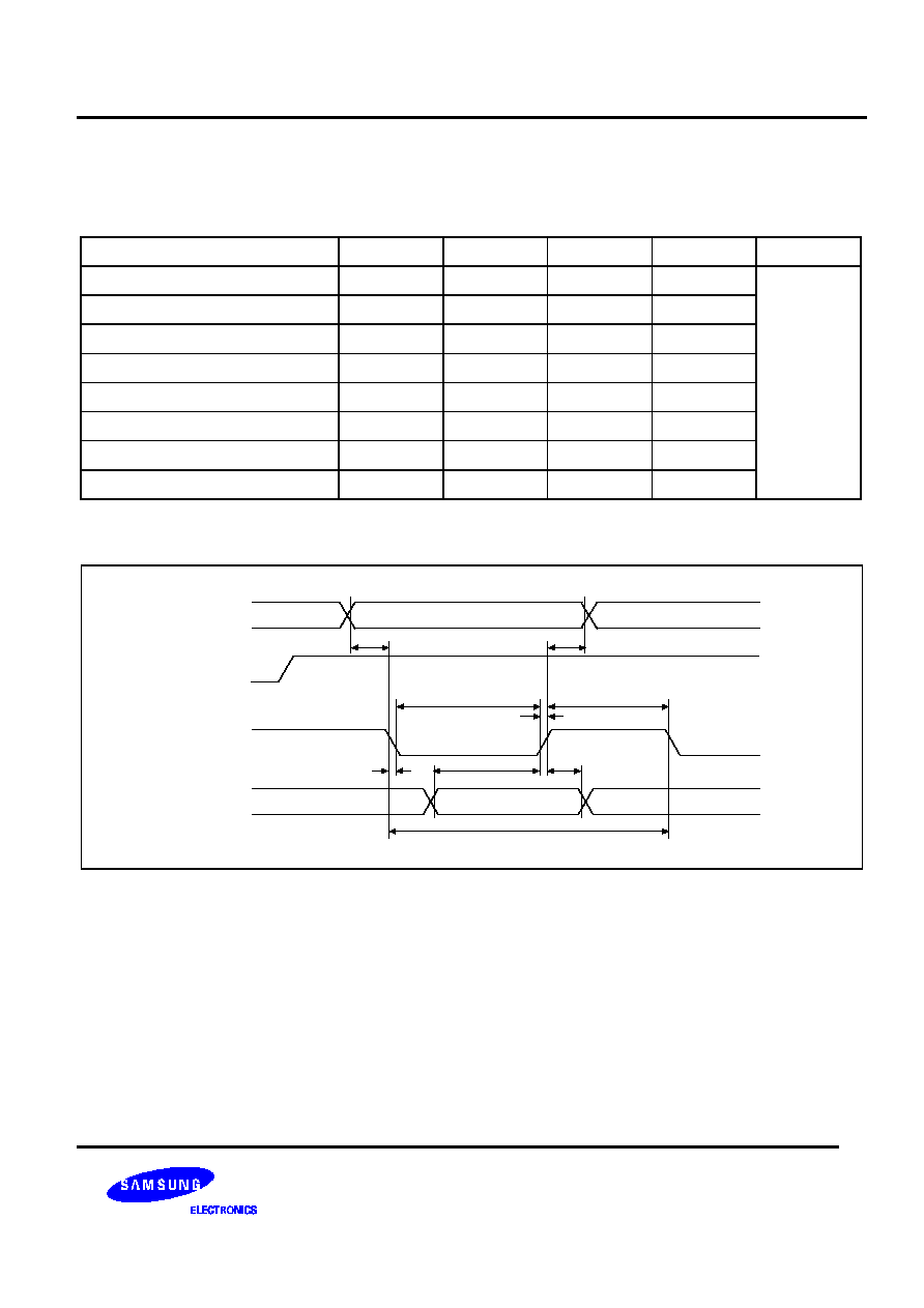
S6D0114 132-RGB X 176-DOT 1-CHIP DRIVER IC FOR 262,144-COLOR TFT-LCD DISPLAY
Preliminary
139
Parallel Write Interface (80 Mode, HWM =1)
Table 51. Parallel Write Interface Characteristic (80 Mode, HWM =1)
(V
DD
= 1.7V to 2.7V, T
A
= -40 to +85
o
C)
Characteristic
Symbol
Min.
Typ.
Max.
Unit
RW_WR cycle time
T
C
62
-
-
Pulse rise / fall time
t
R
,t
F
-
-
3
RW_WR pulse width high
T
WH
30
-
-
RW_WR pulse width low
T
WL
30
-
-
RS and CSB setup time
t
SU1
10
-
-
RS and CSB hold time
t
H1
10
-
-
DB setup time
t
SU2
20
-
-
DB hold time
t
H2
10
-
-
ns
RS,CSB
R W _ W RB
E_RDB
DB17~0
VLD
t
SU1
t
H1
t
W L
t
W H
t
F
t
SU2
t
C
t
H2
t
R
Valid Data
Figure 99. Burst Write Timing Diagram (80-series)
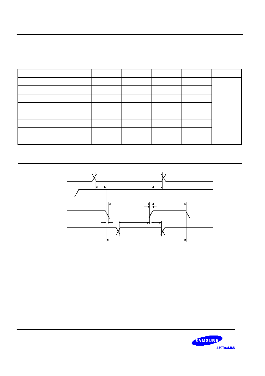
132-RGB X 176-DOT 1-CHIP DRIVER IC FOR 262,144-COLOR TFT-LCD DISPLAY
S6D0114
Preliminary
140
Parallel Write Interface (80 Mode, HWM =0)
Table 52. Parallel Write Interface Characteristic (80 Mode, HWM =0)
(V
DD
= 1.7V to 2.7V, T
A
= -40 to +85
o
C)
Characteristic
Symbol
Min.
Typ.
Max.
Unit
RW_WR cycle time
t
C
250
-
-
Pulse rise / fall time
t
R
,t
F
-
-
10
RW_WR pulse width high
t
WH
100
-
-
RW_WR pulse width low
t
WL
100
-
-
RS and CSB setup time
t
SU1
10
-
-
RS and CSB hold time
t
H1
10
-
-
DB setup time
t
SU2
20
-
-
DB hold time
t
H2
10
-
-
ns
RS,CSB
R W _ W RB
E_RD B
DB17~0
VLD
t
SU1
t
H1
t
W L
t
W H
t
F
t
SU2
t
C
t
H2
t
R
Valid Data
Figure 100. Single Write Timing Diagram (80-series)
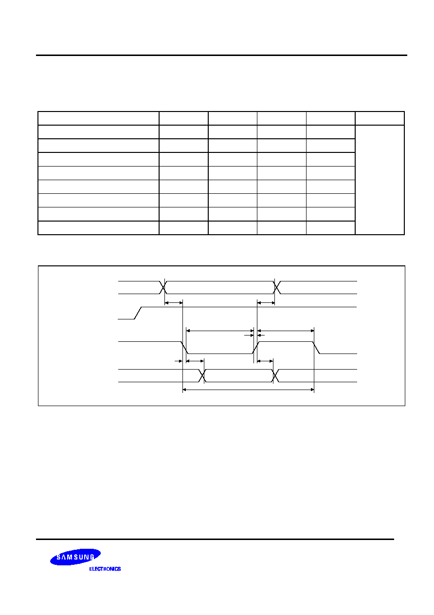
S6D0114 132-RGB X 176-DOT 1-CHIP DRIVER IC FOR 262,144-COLOR TFT-LCD DISPLAY
Preliminary
141
Parallel Read Interface (80 Mode)
Table 53. Parallel Read Interface Characteristic (80 Mode)
(V
DD
= 1.7V to 2.7V, T
A
= -40 to +85
o
C)
Characteristic
Symbol
Min.
Typ.
Max.
Unit
E_RD cycle time
T
C
450
-
-
Pulse rise / fall time
t
R
,t
F
-
-
10
E_RD pulse width high
T
WH
200
-
-
E_RD pulse width low
T
WL
200
-
-
RS and CSB setup time
T
SU
10
-
-
RS and CSB hold time
T
H
10
-
-
DB output delay time
T
D
20
-
-
DB output hold time
T
DH
10
-
-
ns
RS,CSB
R W _ W R
E_RD
DB17~0
t
SU
t
H
t
W L
t
W H
t
F
t
C
t
D
t
DH
Valid Data
t
R
Figure 101. Read Timing Diagram (80-series)
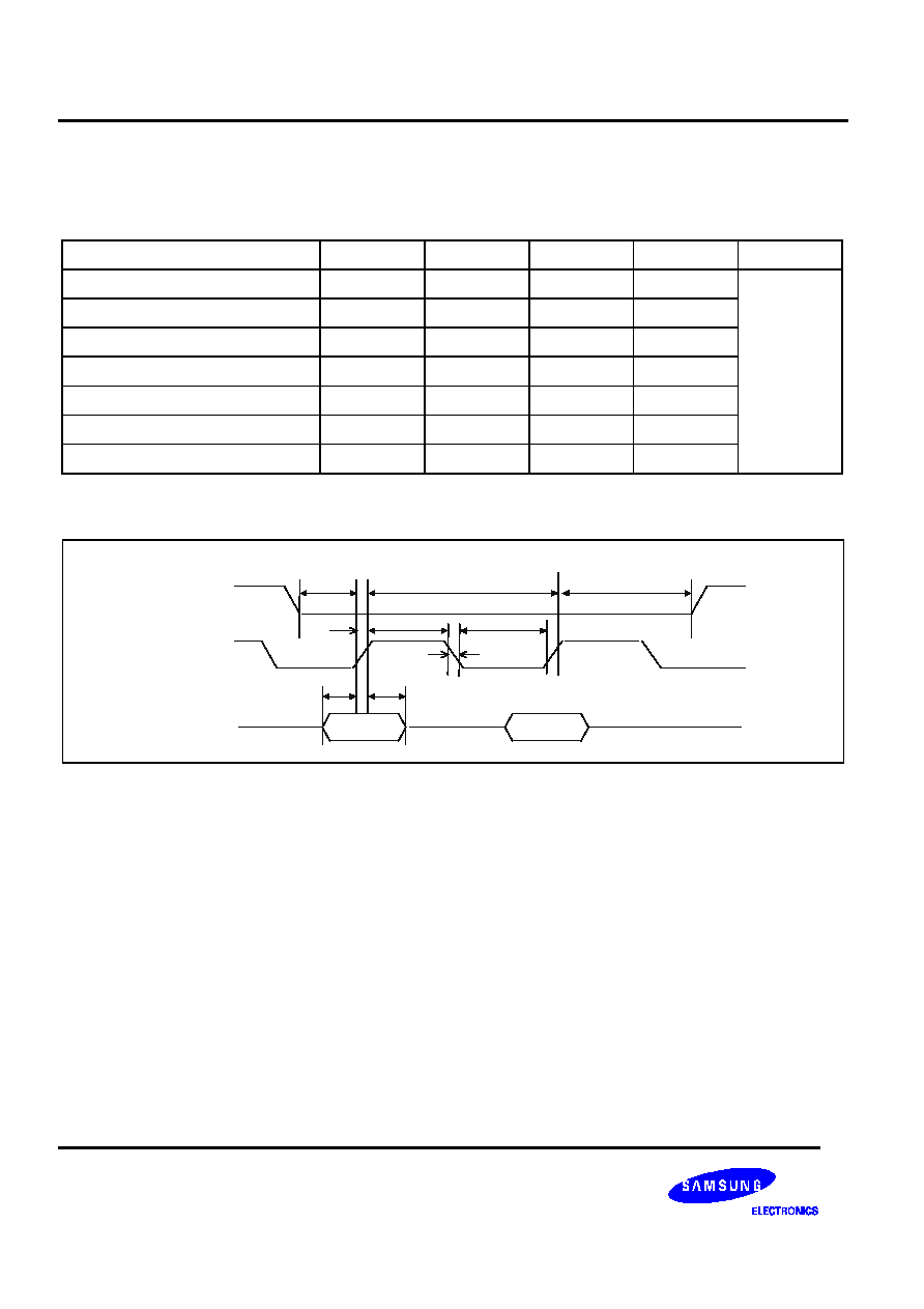
132-RGB X 176-DOT 1-CHIP DRIVER IC FOR 262,144-COLOR TFT-LCD DISPLAY
S6D0114
Preliminary
142
Clock Synchronized Serial Write Mode
Table 54. Clock Synchronized Serial Write Mode Characteristic
(V
DD
= 1.7V to 2.7V, T
A
= -40 to +85
o
C)
Characteristic
Symbol
Min.
Typ.
Max.
Unit
SCL clock cycle time
t
C
20
-
-
Pulse rise / fall time
t
R
,t
F
-
-
3
SCL clock width (high, low)
t
W
7
-
-
CSB setup time
t
SU1
10
-
-
CSB hold time
t
H1
10
-
-
SDI data setup time
t
SU2
5
-
-
SDI data hold time
t
H2
5
-
-
ns
CSB
SCL
SDI
tSU2
tSU1
tH2
t
H1
t
C
t
R
t
W
t
W
t
F
Figure 102. Clock Synchronized Serial Interface Mode Timing Diagram

S6D0114 132-RGB X 176-DOT 1-CHIP DRIVER IC FOR 262,144-COLOR TFT-LCD DISPLAY
Preliminary
143
Clock Synchronized Serial Read Mode
Table 55. Clock Synchronized Serial Read Mode Characteristic
(V
DD
= 1.7V to 2.7V, T
A
= -40 to +85
o
C)
Characteristic
Symbol
Min.
Typ.
Max.
Unit
SCL clock cycle time
t
C
50
-
-
Pulse rise / fall time
t
R
,t
F
-
-
3
SCL clock width (high, low)
t
W
20
-
-
CSB setup time
t
SU1
20
-
-
CSB hold time
t
H1
10
-
-
SDO data delay time
t
D
10
-
-
SDO data delay time
t
DH
10
ns
C S B
S C L
S D O
t
D
t S U 1
t
D H
t
H 1
t
C
t
R
t
W
t
W
t
F
Figure 103. Clock Synchronized Serial Interface Mode Timing Diagram