ENHANCED-1 CHIP CT0 RF IC
KB8528
1
Final version ( 99.4.12 )
INTRODUCTION
KB8528 is a 1 CHIP RF IC which can be used in high performance
CTO CLP systems at max. 60MHz.
KB8528 is designed to include a receiver, PLL and COMPANDER to
minimize PCB space requirements. Improved RX characteristics such
as intermodulation, spurious response and ajacent channel interface
have been included to satisfy the universal standards.
The 1 CHIP RF IC has considerably reduced the cost by including a
build-in 1
'
st mixer, low battery detector, fmcu, RSSI, RF requlator and
speaker amp. Also, it fufills carrier detector threshold control, speaker
volume control, operating mode selection and MUTE function using S/
W, thus makring external application easier.
FEATURES
À
Operating voltage range: 2.0V ~ 5.5V
À
Typical supply current: 8.9mA at 3.6V
À
Built-in low battery detection function ( selectable 3.45V, 3.3V, 3.0V, 2.2V, 2.1V )
À
Built-in speaker volumn control and speaker amplifier
À
Built-in splatter filter
À
Support mode selection ( Active, Rx, Standby and Inactive mode )
À
FM Receiver
--
Excellent Receiver characteristics
--
RSSI ( Linear ) and Carrier detector output ( Digital ) function
À
Compander
--
Easy gain control and application using external component
-- - Included ALC (Automatic Level Control) circuit
À
Universal PLL
--
RX (TX) divided counter range : 1/16 ~ 1/16383
--
Reference frequency divided counter range : 1/16 ~ 1/4095
--
Lock detector signal output
--
Serial interface with MICOM for controlling each block
--
Clock Output for MICOM oscillator substitution. ( X-tal divided clock by 2, 3, 4 and 5 )
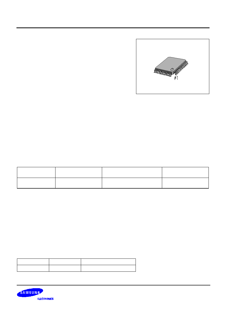
ORDERING INFORMATION
< 10.7MHz crystal filter used >
Input sensitivity
Ajacent channel rejection
Spurious rejection
(image of the second IF)
Intermodulation
rejection
0.7
Á
Vrms at 12dB
SINAD
> 55dB
> 60dB
> 50dB
Device
Package
Operating Temperature
+ KB8528Q
48
-
QFP
-
1010E
-
20C to + 70C
+ : New product
48
-
QFP
-
1010E

KB8528
ENHANCED-1 CHIP CT0 RF IC
2
Final version ( 99.4.12 )
BLOCK DIAGRAM
Limiting
IF AMP
RSSI
Carrier
Detector
Rectifier
Gain Cell
Regulator
(Vcc/2)
Limiter
Gain Cell
Rectifier
IF AMP
(455KHz)
13
14
15
16
17
18
19
21
22
23
Quadrature
Detector
FSK
COMP
ALC
35
38
39
40
41
42
43
44
45
46
47
48
RX
VCO
IF AMP
(10.7MHz)
1st
MIX
PLL Regulator
( 2.05 V )
Programmable Counter ( REF )
RX Phase
Detector
TX Phase
Detector
fMCU
4_25 CNT
CONTROL
Buffer
SUM
AMP
MIC
AMP
SPK
AMP2
SUM
AMP
PRE AMP
AMP
Compander
mute
X-tal
OSC
Low
Battery
Detector
2nd
MIX
36
34
33
32
31
30
29
28
27
26
25
12
11
10
9
8
7
5
4
3
1
2
-
+
VREF
CRC
CO
SFI
SFO
CDO/LDT
CLKO
CLK
DATA
LBD
EN
AGIC
PDT
EPI
ERC
SAI
SAO1
SAO2
VCC
(COMP)
GND
(COMP)
CPI
CPO
ALC
24
V
REF
(COMP)
2MO
VCC
(RX)
LI
LD
GND
(RX)
QCI
RAO
DSCI
DSCO
RSSI
2LOI
6
37
2LOI
GND
(PLL)
V
REF
(RF)
2MI
1LOI
1LOI
1MI
TIF
1MI
1MO
V
REF
(PLL)
VCO
RX
PDR
20 EO
Splatter
Filter
VREF
+
-
Programmable Counter ( RX )
Programmable Counter ( TX )
Internal
cap.
SPK
AMP1
Volume control
VCC
(RX)

ENHANCED-1 CHIP CT0 RF IC
KB8528
3
Final version ( 99.4.12 )
PIN CONFIGURATION
1
2
3
4
5
6
7
8
9
10 11 12
EPI
ERC
EO
SAI
SAO1
SAO2
VCC
(COMP)
GND
(COMP)
CPI
CPO
CRC
2MI
VCC
(RX)
LI
LD
GND
(RX)
QCI
RAO
DSCI
DSCO
RSSI
V
REF(COMP)
ALC
KB8528
14
15
16
17
18
19
20
21
22
23
24
13
47
46
45
44
43
42
41
40
39
38
37
48
36 35 34 33 32 31 30 29 28 27 26 25
CO
SFI
SFO
CDO/LDT
CLKO
CLK
DATA
LBD
EN
AGIC
GND
(PLL)
V
REF(RF)
2MO
2LOI
2LOI
1LOI
1LOI
1MI
TIF
1MI
1MO
V
REF(PLL)
PDT
VCO
RX
PDR
KB8528
ENHANCED-1 CHIP CT0 RF IC
4
Final version ( 99.4.12 )
PIN DESCRIPTION
Pin No
Symbol
Description
1
PDT
Phase detector output terminal of the transmitter at PLL.
If f
TX
> f
REF
or f
TX
is leading
the output is negative pulse
If f
TX
< f
REF
or f
TX
is lagging
the output is positive pulse
If f
TX
= f
REF
and the same phase
the output is High Impedance
2
CO
Compressor output terminal of compander: connected to the splatter filter amp input
terminal.
3
SFI
Input terminal of Splatter filter amp.
4
SFO
Output terminal of Splatter filter amp.
5
LDT/CDO
LDT: Output terminal of transmitter lock detector in PLL block. Output is low if PLL is in
lock state and is high if PLL is in unlock state.
CDO: As an output terminal of the carrier detector buffer, connected to (RSSI ) terminal
of MICOM. This pin outputs the contents of Meter Driver buffer which is turned
on/off, according to the signal level detected by Meter Driver.
6
f
MCU
Clock output terminal for MICOM crystal.
This pin provides the clock source for MICOM or other system as an output of
X-tal osc.
¸
2/
¸
3/
¸
4/
¸
5. Which can be controlled by the bit of the control register.
Clock ON/OFF control is possible by MICOM
7
8
9
CLK
DATA
EN
These pins are serial interface terminals for programming reference counter, auxiliary
reference counter, TX channel counter, RX channel counter and control block that
controls internal each block with 4 mode selection.
10
LBD
Low Battery Detecting output. ( Selectable 3.45V, 3.3V, 3.0V, 2.2V, 2.0V ).
During the normal operation, output level is low, but it is high at low battery detection.
As this pin is an open collector type, it requires a pull-up resister.
11
AGIC
This pin bypasses AC elements at the feedback loop which come from the SUM amp
block of COMPRESSOR. A capacitor should be connected between this terminal and
GND. ( C = 2.2uF )
12
CRC
Converts waveform from the full wave rectifier to DC element at the rectifier block of
Compressor. ( RC = 33 msec at C = 3.3uF)
13
CPO-
Pre-amp output terminal of Compressor.
Used as an input terminal for voice signals.
14
CPI
Inverting type Pre-amp input terminal of Compressor.
15
GND
(COMP
)
Ground.
Ground of Compander.
16
Vcc
(COMP)
Supply voltage.
Power supply terminal of Compander.
17
SAO 2
Output terminal of speaker amp 2.
This signal is the same as SAO1 output, but phase difference is 180
░
for SAO1 DC
voltage level is Vcc / 2.

ENHANCED-1 CHIP CT0 RF IC
KB8528
5
Final version ( 99.4.12 )
18
SAO 1
Output terminal of Speaker amp 1.
DC voltage level is Vcc/ 2.
19
SAI
Speaker Amp 1 input terminal.
Between this terminal and Expander output terminal, apply DC coupled capacitor.
20
EO
Output terminal of Expander
21
ERC
Converts waveform from the full wave rectifier to DC element at the rectifier block of
Expander. ( RC = 33 msec at C = 3.3uF )
22
EPI
Pre-amp inverting input terminal of Expander.
Adjusts the negative feedback loop gain. ( in application, gain is 5 )
23
ALC
Reference current input terminal of Automatic Level Control ( ALC); Adjusts THD of
compressor output voltage to less than 3% or limites the frequency deviation of TX if the
input is higher than a certain level. The ALC circuit may be turned off depending on the
ALC reference current or the magnitude of output voltage may be limited if it is higher
than a certain level.
24
V
REF(COMP)
Reference voltage ( VREF= 1/2 VCC ). Supplies a regulator voltage to the Compressor
and Expander of COMPANDER.
25
RSSI
Received Signal Strength Indicator terminal ( Analog type )
26
DSCO
Output terminal of Data Slicing comparator.
Seperates Frequency Shift Keying ( FSK ) serial data and executes data shapping and
limiting.
27
DSCI
Input terminal of Data slicing comparator.
Non-inverting type with the negative input terminal biased to 1/2 Vcc.
28
RAO
Recovered Audio Output terminal. Voice signals detected by the Quadrature Detector
are amplified and then output through this terminal.
29
QCI
Quadrature coil input terminal.
The 455kHz oscillator circuit is an Lp = 680uH, Cp = 180pF valued LC tank circuit.
Voice signals are detected by mixture of 455kHz ( by phase difference ) which is
converted from mixer 2.
30
GND
RX
Ground .
Ground for Receiver.
31
32
LD
LI
Limiter input and decoupling terminal.
Limiter block removes amplitude modulation elements caused by fading or FM signal
noise. Limiting IF stage makes the second intermediate frequency amplify and limit.
The input impedance of the limiting IF amplifier is set to 1.5k
.
While FM waves are transmitted with constant magnitude, their magnitudes are slightly
modulated due to reflection from obstacles, fading phenomenon, noise wave and
mixing with AM wave elements before entering the receiver
'
s antenna.
The limiter makes amplitude uniform by removing these AM wave elements.
33
V
CC(RX)
Supply voltage.
Supplies power to the Receiver.
PIN DESCRIPTION (Continued)
Pin No
Symbol
Description