1
Video ICs
Single chip Hi-Fi audio signal
processor
BH7800K
The BH7800K incorporates the functions for a VHS audio signal processing system on a single chip. The circuits on
the chip are a peak-noise reduction processor (PNR), an FM modulator / demodulator circuit, an I / O switcher, an
automatic FM detector circuit, an FM bandpass filter, and a regulator circuit.
1) Operates off dual ± power supply which allows a
large reduction in the number of coupling capacitors
required. A built-in regulator makes it easy to con-
struct a power supply system.
2) A two-line SSB (Synchronized Serial Bus) control
decoder circuit is provided, allowing the various IC
modes to be set using serial control.
3) A four line input switcher is included (tuner, BS, and
line 1 / 2). The output switcher can switch between
STEREO, LEFT, and RIGHT, and Hi-Fi, MIX, and
NORMAL, and a BS MONITOR function is also pro-
vided.
4) The PNR processor and FM modulator / demodula-
tor circuit have reversed characteristics at recording
and playback. In addition, the adjustment for carrier
frequency and FM deviation / playback level are
common.
5) The built-in bandpass filter excels at attenuation of
other channels, and can be directly coupled to the
playback amplifier. The FM recording output block
has a high-performance low-pass filter to produce
sine wave output.
6) Slope-control-type FM-switching-noise compensa-
tion circuit.
7) Envelope detector circuit and noise-detector-type
automatic FM detector circuit.
8) VCO that uses the color signal sub-carrier frequency
f
SC
(NTSC: 3.59545MHz, PAL: 4.433619MHz) and
auto-adjusting BPF circuit ensure stable adjustment
with no fluctuation due to mounting stress or time.
·
Absolute maximum ratings (Ta = 25°)
Parameter
Applied voltage
Storage temperature
V
CC
V
EE
V
IN
Tstg
18, 36pin ··························· 6.0
39pin ······························ 6.0
5, 6, 32pin ························
···
6.5
Pins other than the above 6.0
55 ~ + 125
V
Symbol
Limits
Unit
V
V
V
IN
V
Power dissipation
Pd
850
mW
Operating temperature
Topr
10 ~ + 70
°
C
°
C
Reduced by 8.5mW for each increase in Ta of 1
°
C over 25
°
C when mounted on a 70mm
×
70mm, t = 1.6mm glass epoxy board.
·
Features
·
Applications
VCRs

3
Video ICs
BH7800K
·
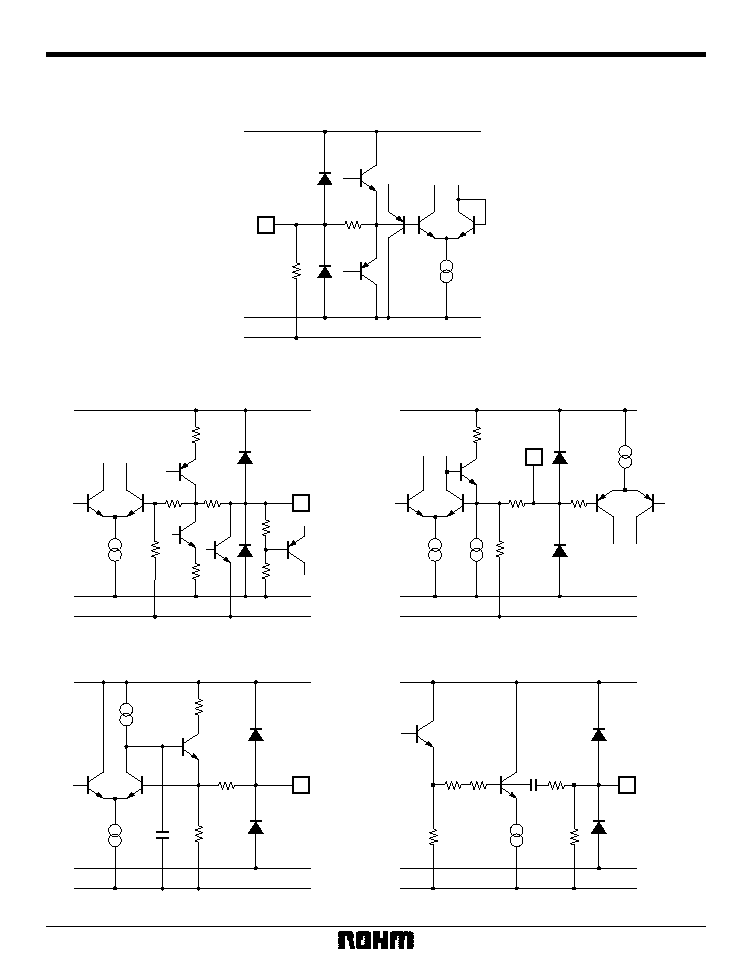
Pin descriptions
Pin No.
Pin name
Format
Voltage
Function
2, 1, 3
TUNER IN L, R, M
150k
0.0V
Tuner input (L, R, M)
4
Hi-Fi ALC
EF (NPN) ~ 200
0.0V
ALC time constant setting for Hi-Fi audio
5
SCL
B (PNP)
--
CLOCK input for SSB control
6
SDA
B (PNP)
--
--
DATA input for SSB bus control
7
GNDD
GND for serial control
8
FSC IN
200k
0.0V
9, 25
NR TC L, R
--
--
--
--
5.0V
f
SC
input for VCO and BPF adjustment
12, 22
DC FB L, R
23k
0.0V
PNR operating reference potential point
15
GNDM
--
0.0V
GND for PNR, MODEM and BPF
16
BPF f
0
ADJ
EF (NPN) ~ 200
1.9V
Center frequency adjustment for FM BPF
17
VCO f
0
ADJ
EF (NPN)
2.5V
VCO control current setting
18
VCCM
--
5.0V
V
CC
for MODEM and BPF
19
FM ALC
EF (NPN) ~ 2.5k
0.0V
FM ALC time constant setting
20
AHSWP IN
B (PNP)
--
Audio head switching pulse input
26
NORMAL IN
100k
0.0V
Normal input
28
MIX OUT
EF (NPN)
0.0V
Mixer amplifier output for RF converter
30, 29
LINE L, R OUT
330
0.0V
Line output
31
NORMAL OUT
EF (P-P)
0.0V
Normal output
32
MUTE CTRL
3k
( > 2.5V)
--
Line output mute control input
34, 33
LINE2 L, R IN
150k
0.0V
Line2 input (L, R)
36
V
CC
--
5.0V
V
CC
regulator
37
ERP
C (NPN)
5.0V
V
CC
regulator error output
38
GND
--
0.0V
I / O switch GND
39
V
EE
--
5.0V
V
EE
regulator
41, 40
LINE1 IN L, R
150k
0.0V
LINE1 input (L, R)
42
ERM
C (PNP)
5.0V
V
EE
regulator error output
44, 43
BS IN L, R
150k
0.0V
BS input (L, R)
PNR attack and recovery time setting
Attack R: 530
, Recovery R: 6.5k
10, 24
WTNG L, R
0.0V
Waiting characteristic, treble time constant (external C = 0.0047
µ
F)
11, 23
NR EMPH L, R
0.0V
NR emphasis time constant setting
(External C = 0.0047
µ
F)
13
FM PB IN
100k
0.0V
Playback FM input 1320mV
P-P
Typ.
Input coupling capacitor (GND ~ V
CC
)
21
FM REC OUT
EF (NPN) ~ 200
3.3V
EE: recording FM output , sine wave output
PB: FM BPF output monitor
27
MIX ALC
EF (NPN) ~ 500
5.0V
ALC time constant setting for mixer amplifier
Attack and recovery time setting
35
VREFP
10k
2.5V
V
CC
/ 2 reference voltage (power on detect and pre-charge functions)
14
/ ADJ FLAG
/ Hi-Fi DET
ENVE OUT
EE: 50k
EE: 0.8V
PB, ADJ: EF (NPN)
PB: 1.0V
FM Lch signal component envelope output
/ Hi-Fi DET output / ADJ FLAG output for ADJ
Note: EF: emitter follower, P-P: push pull, B: base, and C: collector.
All numerical values are standardized values.