BH3856S / BH3856FS
Audio ICs
2-wire serial sound control IC
BH3856S / BH3856FS
The BH3856S and BH3856FS are signal processing ICs designed for volume and tone control in televisions, mini
component stereo systems, and other audio products. Their two-line serial control (I
2
C BUS) enables them to control
volume and tone on the basis of signals from a microcomputer, etc.
!
!
!
!Applications
Televisions, [Video equipped television], personal computer televisions, mini component stereo systems, car stereos.
!
!
!
!Features
1) I
2
C BUS facilitates direct serial control from a microcomputer of volume (main volume), balance (left / right), and tone
(bass, treble). DC control is also possible.
2) Volume is produced by a low-distortion, low-noise VCA. Designed to minimize step noise.
3) Stable standard voltage supply and built-in I/O buffer mean that few attachments are needed. SSOP-A32 package
designed to save space.
4) Matrix surround yields powerful sound.
!
!
!
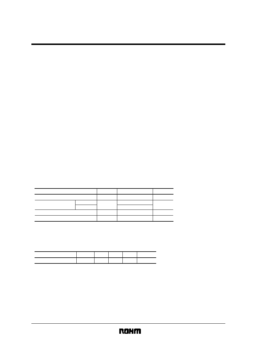
!Absolute maximum ratings
(Ta = 25
°C)
Parameter
Symbol
Limits
Unit
Power supply voltage
10.0
V
Power dissipation
BH3856S
Pd
1200
1
mW
BH3856FS
850
2
Operating temperature
Topr
-
40~
+
85
°
C
Storage temperature
Tstg
-
55~
+
150
°
C
Vcc
1 Reduced by 12mW for each increase in Ta of
1
°
C over 25
°
C.
2 Reduced by 6.8mW for each increase in
Ta of 1
°
C over 25
°
C.
!
!
!
!Recommended operating conditions
(Ta = 25
°C)
Parameter
Symbol
Min.
Typ.
Max.
Unit
Power supply voltage
6.0
9
9.5
V
V
CC
Note : I
2
C BUS is a registered trademark of Philips.

BH3856S / BH3856FS
Audio ICs
!
!
!
!Block diagram
BH3856S
BVN1
IN1
A_GND
BIN1
BVO1
TVN1
TIN1
TVO1
OUT1
V
CC
SC
N.C.
SDA
SCL
D_GND
BVN2
IN2
FILTER
BIN2
BVO2
TVN2
TIN2
TVO2
OUT2
VC1
VC2
TC
BC
V
ref
SLAVE ADDRESS
SELECT SW
2.1k
2.1k
5.1k
5.1k
47k
30k
30k
47k
200k
30k
30k
30k
30k
-
-
Volume
Volume
Reference Voltage
+
-
+
-
+
+
-
-
(Bass) (Treble)
(Bass)
(Treble)
Tone
Matrix surround
Tone
1
2
3
4
5
6
7
8
9
10
11
12
13
14
15
V
CC
Volume
Volume
Control
V
CC
30
29
28
27
26
25
24
23
22
21
20
19
18
17
16
BH3856FS
BVN1
IN1
A_GND
BIN1
BVO1
TVN1
TIN1
TVO1
OUT1
V
CC
SC
N.C.
SDA
SCL
D_GND
BVN2
IN2
FILTER
BIN2
BVO2
TVN2
TIN2
TVO2
OUT2
VC1
VC2
TC
BC
V
ref
SLAVE ADDRESS
SELECT SW
2.1k
2.1k
5.1k
5.1k
47k
30k
30k
47k
200k
30k
30k
30k
30k
-
-
Volume
Volume
Volume
Volume
+
-
-
+
+
-
+
-
(Bass)
(Treble)
Tone
(Bass)
(Treble)
Tone
Matrix surround
N.C.
N.C.
V
CC
Control
V
CC
1
2
3
4
5
6
7
8
9
10
11
12
13
14
15
16
22
21
20
19
18
17
23
24
25
26
27
28
29
30
31
32
Reference Voltage

BH3856S / BH3856FS
Audio ICs
!
!
!
!Pin descriptions
Pin name
Function
1
A_GND
Reference voltage output
2
IN1
3
BVN1
4
BIN1
Time constant pin for prevention of switching shock
BVO1
Time constant pin for prevention of switching shock
Channel 2 volume output
Channel 2 treble filter
Channel 2 treble filter
Channel 2 treble filter
Channel 2 bass filter
Channel 2 bass filter
Channel 2 bass filter
Channel 2 volulme input
Filter
Not connected internally.
6
TVN1
7
TIN1
Channel 1 treble filter
8
TVO1
9
OUT1
10
V
CC
Time constant pin for prevention of switching shock
11
SC
SDA data input pin
12
13
15
16
17
18
19
20
21
22
23
24
25
26
27
28
30
31
32
1
2
3
4
5
6
7
8
9
10
11
13
14
15
16
17
18
19
20
21
22
23
24
25
26
27
28
29
30
12
SDA
SCL
D_GND
SASS
V
ref
BC
TC
VC2
VC1
OUT2
TVO2
TIN2
TVN2
BVO2
BIN2
BVN2
IN2
FILTER
N.C.
SCL data input pin
Digital ground
Slave address selection pin
Time constant pin for prevention of switching shock
Time constant pin for prevention of switching shock
Channel 1 treble filter
Analog ground
Channel 1 volume input
Channel 1 bass filter
Channel 1 bass filter
Channel 1 bass filter
Channel 1 treble filter
Channel 1 volume output
Power supply
Pin No.
BH3856S BH3856FS
5, 14, 29

BH3856S / BH3856FS
Audio ICs
!
!
!
!Input / output circuits
Symbol
Pin voltage
Equivalent circuit
Description
IN1
IN2
4.5V
4.5V
BVN1
BVN2
4.5V
4.5V
4.5V
4.5V
4.5V
4.5V
BIN1
BIN2
BVO1
BVO1
Pin for low band filter connection.
FILTER
5.2V
Main volume input pin.
Designed for input impedance of 47k
Typ.).
Pin for low band filter connection.
Pin for low band filter connection.
Filter input pin.
Please install a capacitor of about 10
µ
F to
the filter pin.
Has built-in precharge and discharge circuits.
A_GND
V
CC
5.1k
2/1V
CC
4pin
28pin
50k
A_GND
V
CC
6pin
27pin
50k
A_GND
3pin
30pin
V
CC
A_GND
V
CC
30k
30k
32pin
47k
A_GND
2pin
31pin
2/1V
CC
V
CC
TVN1
TVN2
4.5V
4.5V
TIN1
TIN2
4.5V
4.5V
Pin for high band filter connection.
Pin for high band filter connection.
25k
A_GND
7pin
26pin
V
CC
A_GND
V
CC
2.1k
2/1V
CC
8pin
25pin
The pin numbers are for the BH3856S.

BH3856S / BH3856FS
Audio ICs
Symbol
Pin voltage
Equivalent Circuit
Description
4.5V
4.5V
4.5V
4.5V
TVO1
TVO2
OUT1
OUT2
Main volume output pin.
OUT1 is the volume output for Channel 1.
OUT2 is the volume output for Channel 2.
SC
BC
TC
VC1
VC2
Pin for high band filter connection.
For prevention of shock noise during
step switching.
SC : Surround pin
BC : Bass pin
TC : Treble pin
VC1 : Volume pin (Channel 1)
VC2 : Volume pin (Channel 2)
25k
A_GND
9pin
24pin
V
CC
A_GND
V
CC
10pin
24pin
A_GND
V
CC
12pin
19pin
20pin
22pin
21pin
Digital
VREF
V
CC
A_GND
D_GND
Power supply voltage pin.
Analog GND pin. Connected to IC board.
Digital GND pin. Separate from Analog GND pin.
V
ref
3.8V
SDA
SCL
SASS
·
I
2
C bass input pin
SDA : serial data line
SCL : serial clock line
·
Slave address selection pin
SASS: slave address selection switch
3.8V regulator output pin.
Output requires capacitor for stopping
oscillation. Output pin has built-in precharge
and discharge circuits, so there is no problem
with start-up or shut-down even with a large
capacitor. This pin is for connection to the
high-band filter.
A_GND
V
CC
18pin
A_GND
V
CC
13pin
15pin
17pin
2k
The pin numbers are for the BH3856S.
-
-
-
-
-