1
Video ICs
2-channel PRE / REC amplifier with
auto-tracking interface
BA7181FS
The BA7181FS is a PRE / REC amplifier developed for use in video cassette recorders. It has been designed for use
in two-head decks and features built-in FB damping, two preamplifiers, a chroma output amplifier, an FM output
amplifier (with AGC), an envelope detector, a constant-current BTL-drive REC amplifier (with AGC)and built-in chan-
nel and REC / PB switches on a single monolithic IC.
·
Applications
VCRs
·
Features
1) The playback amplifier has a total gain of 57dB
(Typ.), and has a low-noise preamplifier. Designed
for VHS-band operation with low external parts
count. The IC has two circuits for two-head VCR
applications.
2) Two playback output systems (through output and
AGC output). The AGC output level is 300mV
P-P
(Typ.);
suitable for FM brightness signal output.
3) Auto-tracking interface is provided for automated
tracking adjustment. The detector characteristic is
linear, and the sensitivity can be adjusted using
external components.
4) The recording amplifier uses constant-current BLT
drive that handles load variations (i.e. head imped-
ance)well, and gives stable recording characteris-
tics. A single circuit is provided for two-head VCR
use.
5) Built-in recording level AGC means adjustment of
FM recording current is not necessary.
6) Head switches for two-channel PRE / REC system
provided.
7) Operates off a single 5V power supply, with low
power dissipation.
·
Absolute maximum ratings (Ta = 25°C)
Parameter
Symbol
Limits
Unit
Applied voltage
Power dissipation
Operating temperature
Storage temperature
V
CC
7.0
V
Pd
937.5
mW
Topr
°
C
Tstg
°
C
When mounted on a 90mm
×
50mm, t = 1.6mm glass epoxy board.
Reduced by 7.5mW for each increase in Ta of 1
°
C over 25
°
C.
20 ~ + 65
55 ~ + 150
·
Recommended operating (Ta = 25°C)
Parameter
Symbol
Min.
Typ.
Max.
Unit
Conditions
Playback / recording (voltage range)
V
CC
4.5
5.0
5.5
V
11pin
Not designed for radiation resistance.
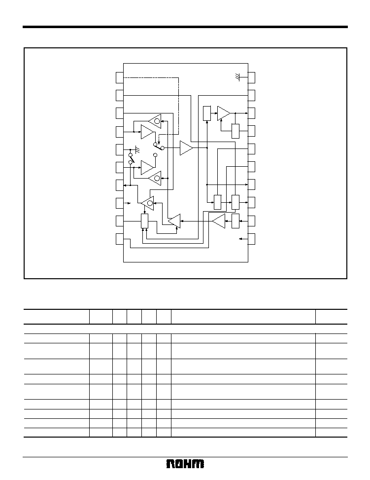
2
Video ICs
BA7181FS
·
Block diagram
123
456789
1
0
11
12
13
14
15
16
17
18
19
20
+
RF
PRE
DET
AGC
PRE
LOGIC
ENVE
PEAK
MUTE
REC
AGC
HPF
DET
(REC - OUT 1)
(REC - OUT 2)
DFF IN
DET FILTER
REC DCFB
PRE IN 1
GND 1
PRE IN 2
PB / EE / REC CTRL
REC + OUT
REC AGC FILTER
AT ENVE FB
GND 2
REC LEVEL ADJ
PB AGC OUT
PB AGC FILTER
AT ENVE PEAKING
H SYNC IN
PB RF OUT
AT ENVE OUT
REC IN
V
CC
V
CC
·
Electrical characteristics (unless otherwise noted, Ta = 25°C, V
CC
= 5.0V and f = 4.0MHz)
Parameter
Symbol Min. Typ. Max. Unit
Conditions
Measurement
circuit
Playback system
Quiescent current
Voltage gain CH-1
Voltage gain CH-2
Voltage gain differential
Frequency characteristic
2nd harmonic distortion
3rd harmonic distortion
Maximum output level
Crosstalk
Iq
(P)
--
18
45
mA
Fig.1
G
VP1
54
57
60
dB
Fig.1
G
VP2
54
57
60
dB
Fig.1
G
VP
--
0
1
dB
Fig.1
G
Vf
7
3
0
dB
Fig.1
2HD
P
-- 45
--
dBc
Fig.1
3HD
P
-- 45
--
dBc
Fig.1
V
OMP
1.0
1.5
--
V
P-P
Fig.1
CT
P
-- 38 32
dBc
Fig.1
No signal
Pin 4 input = 0.3mV
P-P
, pin 1: L,
pin 14 output measurement
Pin 6 input = 0.3mV
P-P
, pin 1: H,
pin 14 output measurement
G
VP
= | G
VP1
--G
VP2
|
Difference in pin 14 output level for f = 8.0 / 1.0MHz,
V
IN
= 0.3mV
P-P
V
IN
= 0.3mV
P-P
, 8.0MHz spurious
V
IN
= 0.3mV
P-P
, 12.0MHz spurious
When pin 14 output 2nd harmonic distortion is 30dBc
Difference in pin 14 output level for pin 1: H / L
Design reference values.
(Fig. 1 measurement circuit, pin 8: "H" )
3
Video ICs
BA7181FS
Note: dBc: dB below carrier (used to express relative level from carrier reference for convenience sake).
Design reference values.
Parameter
Symbol Min.
Typ. Max.
Unit
Conditions
Playback system
Output DC offset
Input conversion noise
AGC output level
AGC control sensitivity
AGC amp frequency
characteristic
PB switch ON resistance
PRE CH 2 threshold voltage
PRE CH 1 threshold voltage
ENVE residual voltage
ENVE output level
ENVE saturation voltage
PB mode holding voltage
EE mode holding voltage
REC mode holding voltage
Pin 14 output DC offset for pin 1: H / L
Rg = 10
, input conversion of pin 14 output noise
V
IN
= 0.3mV
P-P
, pin 18 output measurement
Pin 18 output difference for V
IN
= 0.15
~ 0.6mV
P-P
Pin 18 output level difference for
f = 8.0 / 1.0MHz, V
IN
= 0.3mV
P-P
Pin 7 impedance
Pin 1 DC voltage for channel 2 operation
Pin 1 DC voltage for channel 1 operation
Pin 13 output measurement with no signal
Pin 13 output measurement when pin 14
output = 400mV
P-P
Pin 13 output measurement for large signal
Pin 8 DC voltage for PB mode
Pin 8 DC voltage for REC MUTE mode
Pin 8 DC voltage for REC mode
V
ODC
--
0
150 mV
P-P
Fig.1
V
NIN
--
0.25
--
µ
V
rms
Fig.1
V
AGC
250
300
350 mV
P-P
Fig.1
V
AGC
--
0.3
2.0
dB
Fig.1
G
VAF
--
0.5
--
dB
Fig.1
R
ON7
--
4
--
Fig.1
V
TH1H
3.5
--
V
CC
V
Fig.1
V
TH1L
0
--
1.2
V
Fig.1
V
ENV1
--
0.7
1.0
V
Fig.1
V
ENV2
2.4
2.9
3.4
V
Fig.1
V
ENV3
4.0
4.5
--
V
Fig.1
V
TH10H
3.8
--
V
CC
V
Fig.1
V
TH10M
2.2
--
2.8
V
Fig.1
V
TH10L
0
--
1.2
V
Fig.1
Measurement
circuit
(Fig. 1 measurement circuit, pin 8: "H" )
(unless otherwise noted, Ta = 25°C, V
CC
= 5.0V, f = 4.0MHz and I
OAR
= 30mA
P-P
)
Parameter
Symbol Min.
Typ.
Max.
Unit
Recording system
Supply current
Recording AGC level
AGC control sensitivity
REC Amp frequency
characteristic
2nd harmonic distortion
3rd harmonic distortion
Cross modulation distortion
Maximum output level
Recording current load
characteristic
Mute attenuation ratio
AGC mode holding voltage
AGC mode holding voltage
Iq
(R)
--
72
110
mA
P-P
Fig.2
I
OAR
27
30
33
mA
Fig.2
I
OAR
--
0.3
1.5
dB
Fig.2
I
OAF
--
1.5
--
dB
Fig.2
2HD
R
--
45
--
dBc
Fig.2
3HD
R
--
50
--
dBc
Fig.2
CMD
R
--
50
--
dBc
Fig.2
I
OMR
40
50
--
mA
P-P
Fig.2
I
ORL
--
0.35
--
dB
Fig.2
MU
R
--
45
38
dBc
Fig.2
V
TH15H
2.7
--
V
Fig.2
V
TH15L
0
--
1.2
V
Fig.2
No signal
Pin 12 input = 125mV
P-P
, pin 7 output measurement
Pin 7 output level difference for pin 12
input = 62.5mV
P-P
and 250mV
P-P
Pin 7 output level difference for f = 8.0 / 1.0MHz,
pin 12 input = 125mV
P-P
Pin 12 input = 125mV
P-P
, 8MHz spurious
Pin 12 input = 125mV
P-P
, 12.0MHz spurious
4.0MHz
±
630kHz spurious
When pin 7 output 2nd harmonic distortion is 30dB
Pin 7 output level difference for load L: 8.2 ~ 12
µ
H
Pin 7 output level difference for pin 8: M / H
Pin 15 DC voltage to maintain recording AGC operation
Pin 15 DC voltage to maintain recording AGC stopped
Conditions
V
CC
Measurement
circuit
(Pin 8 in Fig. 2 measurement circuit "L" )
Design reference values.

4
Video ICs
BA7181FS
·
Measurement circuits
(Playback system)
DFF IN
L: REC MUTE
L: REC START
AT ENVE OUT
PB RF OUT
H SYNC IN
PB AGC OUT
REC LEVEL ADJ
43k
0.1
µ
3.9k
22
µ
390k
0.01
µ
470pF
0.1
µ
0.1
µ
39k
10k
33k
REC IN
0.1
µ
10
10
1k
1k
0.1
µ
1
2
3
4
5
6
7
8
9
10
11
12
13
14
15
16
17
18
19
20
+
RF
PRE
DET
AGC
PRE
LOGIC
ENVE
MUTE
REC
AGC
HPF
DET
EP "H"
68p
PRE IN 1
PRE IN 2
AT ENVE GAIN
PEAK
V
CC
V
CC
5V
PB / EE / REC CTRL
F
H
[ ]
[ ]
[
]
Units: R
C
L
Fig.1
+

5
Video ICs
BA7181FS
(Recording system)
DFF IN
L: REC MUTE
L: REC START
AT ENVE OUT
PB RF OUT
H SYNC IN
PB AGC OUT
REC LEVEL ADJ
43k
0.1
µ
3.9k
22
µ
390k
0.01
µ
470pF
0.1
µ
0.1
µ
39k
10k
33k
REC IN
10
REC
OUT
8.2
µ
8.2
µ
0.1
µ
0.1
µ
1
2
3
4
5
6
7
8
9
10
11
12
13
14
15
16
17
18
19
20
+
RF
PRE
DET
AGC
PRE
LOGIC
ENVE
MUTE
REC
AGC
HPF
DET
PP / EE / REC CTRL
EP "H"
68p
AT ENVE GAIN
V
CC
5V
V
CC
PEAK
Fig.2
+
F
H
[ ]
[ ]
[
]
Units: R
C
L